background image

NEO-F10N - Integration manual

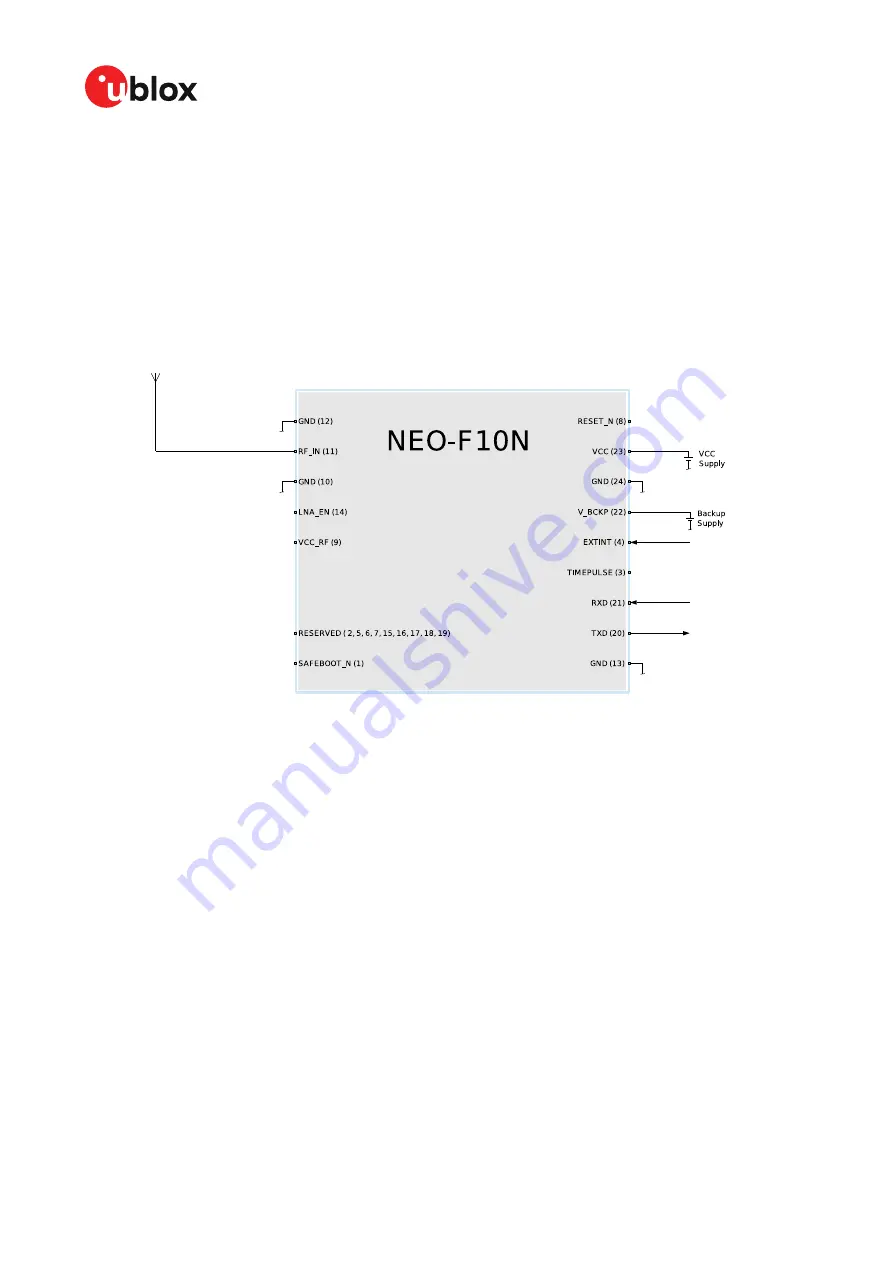
• V_BCKP  supply  is  optional.  If  present,  the  hardware  backup  mode  is  supported.  This  mode

maintains the RTC time and GNSS orbit data in the battery-backed RAM memory if the main
supply is switched off.
If there is no backup supply, time aiding with the UBX-MGA-INI-TIME_UTC message (optionally
with a timing signal at the EXTINT pin) and the GNSS orbit data from the AssistNow services or
stored on the host controller can be used to reduce the TTFF.

• For  an  absolute  minimum  design,  all  the  PIOs  (RESET_N,  EXTINT,  TIMEPULSE,  LNA_EN,  and

SAFEBOOT_N) can be left open.

Figure 14: Typical design

B.2 Active antenna design

Here are some key features for a NEO-F10N design with an active antenna:
• Designs using active antennas must not exceed 25 dB gain. For antenna gain above 25 dB, the

internal LNA mode can be changed to low-gain or bypass mode.

• The active antenna can be supplied either with the VCC_RF output from NEO-F10N as shown in

Figure 16

 or from an external supply as shown in 

Figure 15

. In both figures the supply is controlled

by the LNA_EN signal. The LNA_EN signal combined with the dual MOSFET switches on/off the
antenna power supply when VCC supply is removed or during software standby mode, saving the
antenna power consumption during the off periods.

• Designs using the VCC_RF output to supply the GNSS antenna require a current limiter circuitry

in case of short circuit on the antenna side. 

Figure 16

 shows the required components. The R17

resistor value defines the maximum current in case of antenna short circuit.

UBXDOC-963802114-12193 - R02


Appendix

Page 37 of 42

C1-Public

Summary of Contents for NEO-F10N

Page 1: ...al grade Integration manual Abstract This document describes the features and application of the u blox NEO F10N module an L1 L5 dual band GNSS receiver for meter level accuracy in urban environment w...

Page 2: ...logos and designs included in this document Copying reproduction or modi cation of this document or any part thereof is only permitted with the express written permission of u blox Disclosure to third...

Page 3: ...t lters 12 2 2 3 Navigation output lters 13 2 2 4 Odometer lters 13 2 2 5 Static hold 14 2 2 6 Freezing the course over ground 15 3 Receiver functionality 17 3 1 Communication interfaces and PIOs 17 3...

Page 4: ...Appendix 34 A Migration 34 A 1 Hardware changes 34 A 2 Software changes 35 B Reference designs 36 B 1 Typical design 36 B 2 Active antenna design 37 C External components 39 C 1 Standard capacitors 39...

Page 5: ...view The NEO F10N module features the u blox F10 GNSS multi band platform and provides exceptional sensitivity and acquisition time with unparalleled low power consumption for L1 and L5 GNSS signals 1...

Page 6: ...ved Not connected 7 Reserved Not connected 8 RESET_N I RESET active low 9 VCC_RF O Output voltage RF section 10 GND Ground 11 RF_IN I GNSS signal input 12 GND Ground 13 GND Ground 14 LNA_EN O On O int...

Page 7: ...Reserved Not connected 18 Reserved Not connected 19 Reserved Not connected 20 TXD O UART TX 21 RXD I UART RX 22 V_BCKP I Backup voltage supply 23 VCC I Supply voltage 24 GND Ground Table 1 NEO F10N p...

Page 8: ...reset resetMode 0x00 and 0x04 Flash Permanent storage of the con guration settings A UBX CFG CFG message to erase the con guration on the ash layer Table 2 Permanence of storage and clearing actions f...

Page 9: ...guration in the ash memory Con guring the internal LNA mode in the ash memory 1 Power up the system 2 Test the communication interface by polling the UBX MON VER message 3 Send the con guration strin...

Page 10: ...stored in the BBR and ash layers send the UBX CFG RST message with resetMode 0x01 To revert back to the default con guration send the con guration string given in Table 5 The device returns the UBX AC...

Page 11: ...r rate than the navigation data The output rate for each message is de ned in the CFG MSGOUT con guration group If the output rate of the message is set to one 1 on the UART interface CFG MSGOUT UBX_N...

Page 12: ...g 80000 250 10000 Altitude Large Airborne 4g 80000 500 20000 Altitude Large Wrist 9000 30 20 Altitude and velocity Medium Table 8 Dynamic platform model details Applying dynamic platform models design...

Page 13: ...marked as valid should not be used UBX NAV STATUS message also reports whether a x is valid in the gpsFixOK ag These messages have only been retained for backwards compatibility and it is recommended...

Page 14: ...the position wander caused by environmental factors such as multi path and improves position accuracy especially in stationary applications By default the static hold mode is disabled The CFG MOT GNSS...

Page 15: ...racy for example with bad signals or if the absolute speed value is very low under 0 1 m s the course over ground value becomes inaccurate too In this case the course over ground value is frozen that...

Page 16: ...NEO F10N Integration manual Figure 5 Flowchart of course over ground freezing UBXDOC 963802114 12193 R02 2 Receiver con guration Page 16 of 42 C1 Public...

Page 17: ...when the UART RX interface is re enabled at the end of the one second period Baud rate Data bits Parity Stop bits 4800 8 none 1 9600 8 none 1 19200 8 none 1 38400 8 none 1 57600 8 none 1 115200 8 non...

Page 18: ...FEBOOT_N functions share the same internal IC function If this pin is low at receiver startup the receiver will enter safeboot mode However in normal operation the pin outputs the time pulse signal Ma...

Page 19: ...brMask eld in the UBX CFG RST message to initiate hot warm and cold starts or a combination of startup modes The reset type can also be speci ed This is not related to GNSS but to the way the software...

Page 20: ...ode allows entering a backup state and resuming operation by switching the main power supply on and o while maintaining a V_BCKP supply via e g a battery V_BCKP must be supplied to maintain the backup...

Page 21: ...ut the V_BCKP pin is supplied the receiver enters the hardware backup mode In this mode the RTC time and the GNSS orbit data in the BBR are maintained Valid time and GNSS orbit data at startup improve...

Page 22: ...BBR and ash layers using the con guration item CFG HW RF_LNA_MODE and applying a reset Once in production the ash layer can be con gured to automatically apply the con guration at every startup For mo...

Page 23: ...evel and the immunity of the receiver The maximum power coupled into the receiver RF input is compared against the immunity limit of the receiver de ned in Out of band blocking immunity 4 2 4 Antenna...

Page 24: ...d from any other digital circuits on the system board To achieve this position the receiver digital part towards the digital section of the system PCB and place the RF section and antenna as far away...

Page 25: ...recision GNSS module needs to have as low an impedance as possible with large vias to the lower power layer of the PCB The VCC pad needs a large pad and the decoupling capacitor must be placed as clos...

Page 26: ...provide recommendations for the paste mask Note that the copper and solder masks have the same size and position Figure 9 Recommended copper land and solder mask opening for NEO F10N To improve the we...

Page 27: ...NEO F10N Integration manual Figure 10 Recommended paste mask pattern for NEO F10N UBXDOC 963802114 12193 R02 4 Hardware integration Page 27 of 42 C1 Public...

Page 28: ...mple patch antenna 10 pF coax cable 50 80 pF m or soldering iron To prevent electrostatic discharge through the RF input do not touch any exposed antenna area If there is any risk that such exposed an...

Page 29: ...hey are shipped on reel type B as speci ed in the u blox Packaging information reference 4 5 2 2 Tapes Figure 11 shows the feed direction and illustrates the orientation of the components on the tape...

Page 30: ...ldering paste is highly recommended as it does not require cleaning after the soldering process The paste in the example below meets these criteria Soldering paste OM338 SAC405 Nr 143714 Cookson Elect...

Page 31: ...mit time above 217 C liquidus temperature 40 60 s Peak re ow temperature 245 C Cooling phase A controlled cooling prevents negative metallurgical e ects of the solder solder becomes more brittle and p...

Page 32: ...e ow soldering cycle due to lack of adhesion The module can also tolerate an additional re ow cycle for rework purposes Wave soldering Base boards with combined through hole technology THT components...

Page 33: ...u blox makes no warranty for damages to the module caused by soldering metal cables or any other forms of metal strips directly onto the EMI covers Use of ultrasonic processes Some components on the...

Page 34: ...s of peak current I_VCC is slightly higher in u blox F10 than in u blox 8 M8 Ensure that the power supply is still able to provide clean and stable voltage with the higher current demand in NEO F10N P...

Page 35: ...evious NEO M8 designs to support L5 frequency band GPS L5 New signal Code change optional BeiDou B1C New signal BeiDou satellite IDs up to 63 supported Code change optional BeiDou B2a New signal BeiDo...

Page 36: ...hip identi er output in boot screen and in the UBX SEC UNIQID message Code change optional Con guration lock New security feature that is enabled with CFG SEC CFG_LOCK message for locking the receiver...

Page 37: ...tenna Designs using active antennas must not exceed 25 dB gain For antenna gain above 25 dB the internal LNA mode can be changed to low gain or bypass mode The active antenna can be supplied either wi...

Page 38: ...manual Figure 15 Design with active antenna controlled by LNA_EN signal Figure 16 Design with active antenna supplied by VCC_RF and controlled by LNA_EN signal UBXDOC 963802114 12193 R02 Appendix Pag...

Page 39: ...to supply antenna through VCC_RF 220 5 0 1 W R20 Current limiter to supply antenna through VCC_RF 2 2 k 5 0 1 W Table 16 Standard resistors C 3 Inductors Table 17 presents the recommended inductor val...

Page 40: ...114 12318 3 u blox F10 SPG 6 00 Interface description UBX 23002975 4 u blox Packaging information reference UBX 14001652 For regular updates to u blox documentation and to receive product change noti...

Page 41: ...s comments R01 05 Sep 2023 Initial release R02 07 Nov 2023 Added sections GPS L5 signal health status con guration LNA_EN Updated sections Block diagram Pin assignment Internal LNA modes Migration UBX...

Page 42: ...gration manual Contact u blox AG Address Z rcherstrasse 68 8800 Thalwil Switzerland For further support and contact information visit us at www u blox com support UBXDOC 963802114 12193 R02 Page 42 of...

Reviews: