background image

TOBY-L4 series - System Integration Manual 

UBX-16024839 - R04 


Approvals 


Page 130 of 143


4.4


European Conformance CE mark 

TOBY-L4906 modules have been evaluated against the essential requirements of the Radio Equipment Directive 
2014/53/EU. 
In  order  to  satisfy  the  essential  requirements  of  the  2014/53/EU  RED,  the  modules  are  compliant  with  the 
following standards: 


Radio Spectrum Efficiency (Article 3.2): 

o


EN 301 511  

o


EN 301 908-1  

o


EN 301 908-2  

o


EN 301 908-13  


Electromagnetic Compatibility (Article 3.1b): 

o


EN 301 489-1  

o


EN 301 489-52 


Health and Safety (Article 3.1a) 

o


EN 60950-1 

o


IEC 62368-1 and EN 62368-1 


Radiofrequency  radiation  exposure  information:  this  equipment  complies  with  radiation 
exposure limits prescribed for an uncontrolled environment for fixed and mobile use conditions. 
This equipment should be installed and operated  with a minimum distance of 20 cm between 
the  radiator  and  the  body  of  the  user  or  nearby  persons.  This  transmitter  must  not  be  co-
located or operating in conjunction with any other antenna or transmitter except as authorized 
in the certification of the product. 


The  gain  of  the  system  antenna(s)  used  for  the  TOBY-L4906  modules  (i.e.  the  combined 
transmission  line,  connector,  cable  losses  and  radiating  element  gain)  must  not  exceed  the 
following values for mobile and fixed or mobile operating configurations: 

o


2.9 dBi in the 900 MHz band, i.e. GSM 900 or UMTS FDD-8 band 

o


8.8 dBi in the 1800 MHz band, i.e. GSM 1800 or LTE FDD-3 band 

o


12.7 dBi in the 1900 MHz band, i.e. LTE TDD-39 band 

o


12.3 dBi in the 2100 MHz band, i.e. UMTS FDD-1 or LTE FDD-1 band 

o


13.0 dBi in the 2300 MHz band, i.e. LTE TDD-40 band 

o


13.0 dBi in the 2500 MHz band, i.e. LTE TDD-41 band 

 
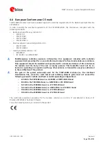
The  conformity  assessment  procedure  for  the  modules,  referred  to  in  Article  17  and  detailed  in  Annex  II  of 
Directive 2014/53/EU, has been followed. 
Thus, the following marking is included in the product: 


Summary of Contents for TOBY-L4 Series

Page 1: ...mode cellular modules The modules are a complete and cost efficient LTE FDD LTE TDD DC HSPA E GPRS multi mode and multi band solution with uCPU embedded Linux programming capability The modules offer...

Page 2: ...06 50A 00 40 24 A00 02 UBX 18007908 Engineering Sample TOBY L4206 TOBY L4206 00A 00 TBD TBD TBD Functional Sample TOBY L4206 50A 00 TBD TBD TBD Functional Sample TOBY L4906 TOBY L4906 00A 00 TBD TBD T...

Page 3: ...Integration Manual provides the necessary information to successfully design and configure the u blox cellular modules This manual has a modular structure It is not necessary to read it from the begi...

Page 4: ...le host configuration selection 35 1 7 Antenna interfaces 36 1 7 1 Antenna RF interfaces ANT1 ANT2 36 1 7 2 Antenna detection interface ANT_DET 38 1 8 SIM interfaces 38 1 8 1 SIM interfaces 38 1 8 2 S...

Page 5: ...e 86 2 6 2 UART interfaces 89 2 6 3 SPI interfaces 93 2 6 4 DDC I 2 C interfaces 94 2 6 5 SDIO interface 98 2 6 6 RGMII interface 100 2 7 eMMC interface 101 2 8 Audio interface 102 2 8 1 Analog audio...

Page 6: ...ration of conformity 125 4 2 3 Modifications 126 4 3 Innovation Science and Economic Development Canada notice 127 4 3 1 Declaration of Conformity 127 4 3 2 Modifications 128 4 4 European Conformance...

Page 7: ...Y L4906 modules mainly designed for operation in China TOBY L4 series modules include the following product versions The 00 product versions integrating the u blox uCPU on chip processor to allow cust...

Page 8: ...FOTA Dual stack IPv4 IPv6 Standard Professional Automotive TOBY L4006 00 North America 2 4 5 7 12 13 29 2 4 5 850 1900 4 1 1 2 1 1 1 2 2 14 2 TOBY L4006 50 North America 2 4 5 7 12 13 29 2 4 5 850 190...

Page 9: ...ta rate GPRS multi slot class 33 CS1 CS4 up to 107 0 kbit s DL up to 85 6 kbit s UL EDGE multi slot class 33 MCS1 MCS9 up to 296 0 kbit s DL up to 236 8 kbit s UL Table 2 TOBY L4 series LTE 3G and 2G...

Page 10: ...of the module via power amplifier PA SAW band pass filters band specific duplexer and antenna switch Dual receiving paths are implemented according to Carrier Aggregation MIMO and Receiver Diversity...

Page 11: ...l paths o Memory interface controller o Dedicated peripheral blocks for control of the USB SIM and generic digital interfaces o Interfaces to the RF transceiver ASIC Memory system which includes NAND...

Page 12: ...esistor to internal 1 3 V supply rail Test Point for diagnostic access is recommended See section 1 6 1 for functional description See section 2 3 1 for external circuit design in RESET_N 23 I Externa...

Page 13: ...n in SIM1_RST 177 O SIM1 reset Reset output for 1 8 V 3 V SIM See section 1 8 for functional description See section 2 5 for external circuit design in USB VUSB_DET 4 I USB detect input VBUS 5 V typic...

Page 14: ...or functional description See section 2 6 2 for external circuit design in TXD 16 I UART0 data input 1 8 V input Circuit 103 TXD in ITU T V 24 Internal active pull up to V_INT Test Point for diagnosti...

Page 15: ...See section 2 6 2 for external circuit design in TXD2 161 I UART2 data input 1 8 V input Circuit 103 TXD in ITU T V 24 Internal active pull up to V_INT See section 1 9 2 for functional description Se...

Page 16: ...n with Wi Fi Bluetooth See section 1 9 5 for functional description See section 2 6 5 for external circuit design in Ethernet V_ETH 221 O Ethernet Interface supply output Ethernet RGMII RMII interface...

Page 17: ...the detection of an interrupt event in the PHY See section 1 9 6 for functional description See section 2 6 6 for external circuit design in ETH_MDIO 222 I O Ethernet Management Data Input Output Eth...

Page 18: ...functional description See sections 2 8 for external circuit design in I2S1_CLK 208 I O I2S1 clock I2 S serial clock See sections 1 11 for functional description See sections 2 8 for external circuit...

Page 19: ...s Configurable as External Interrupt by uCPU API See section 1 13 for functional description See section 2 10 for external circuit design in GPIO4 25 I O GPIO 1 8 V GPIO with alternatively configurabl...

Page 20: ...uration enabled by AT UPSV command or uCPU API The modules automatically switch from the active mode to low power idle mode whenever possible if power saving is enabled The modules wake up from low po...

Page 21: ...r a defined time interval Any wake up event described in the module operating modes summary table above Incoming outgoing call or other dedicated device network communication No RF Tx Rx in progress C...

Page 22: ...supply V_MMC eMMC interface supply and any other internal rail During operation the current drawn by the TOBY L4 series modules through the VCC pins can vary by several orders of magnitude This range...

Page 23: ...adequate margin the highest averaged VCC current consumption value in connected mode conditions The maximum average current consumption can be greater than the specified value according to the actual...

Page 24: ...ne in the low bands due to the 3GPP transmitter output power specifications During a GSM call current consumption is not so significantly high in receiving or in monitor bursts and is low in the inact...

Page 25: ...ion figures are quite less high than the one in the low bands due to 3GPP transmitter output power specifications Figure 6 reports the current consumption profiles in GPRS class 12 connected mode in t...

Page 26: ...enario corresponding to a continuous transmission and reception at maximum output power approximately 250 mW or 24 dBm the average current drawn by the module at the VCC pins is considerable At the lo...

Page 27: ...ly enabled in FDD In the worst case scenario corresponding to a continuous transmission and reception at maximum output power approximately 250 mW or 24 dBm the average current drawn by the module at...

Page 28: ...n active mode The time period between two paging block receptions is defined by the network This is the paging period parameter fixed by the base station through the broadcast channel sent to all user...

Page 29: ...saving mode Figure 10 illustrates a typical example of the module current consumption profile when power saving is disabled In such a case the module is registered with the network and while active mo...

Page 30: ...odule main supply is not applied to the VCC pins the RTC is supplied from a small bypass capacitor mounted inside the module However this small capacitor is not able to provide a long buffering time w...

Page 31: ...p resistor to an internal 1 3 V supply rail the PWR_ON input voltage thresholds are different from the other generic digital interfaces and the line should be driven by an open drain by an open collec...

Page 32: ...set state to the default operational configured state The duration of this pins configuration phase differs within the generic digital interfaces and the USB interface due to host device enumeration t...

Page 33: ...o perform a clean network detach It is highly recommended to avoid an abrupt removal of the VCC supply during TOBY L4 series modules normal operations the switch off procedure must be started by an ap...

Page 34: ...T Then the module remains in power off mode as long as a switch on event does not occur i e applying a suitable low level pulse to the PWR_ON input pin and enters not powered mode if the supply is rem...

Page 35: ...emory and a clean network detach is not performed It is highly recommended to avoid an abrupt hardware reset of the module by forcing a low level on the RESET_N input during modules normal operation t...

Page 36: ...requency Range See the TOBY L4 series Data Sheet 1 The required frequency range of the antenna connected to the ANT1 port depends on the operating bands of the used cellular module and the used mobile...

Page 37: ...ed performance requirements as the TIS specified by applicable related certification schemes Table 9 Summary of secondary Rx antenna RF interface ANT2 requirements Item Requirements Remarks Efficiency...

Page 38: ...the u blox AT Commands Manual 2 or by means of the uCPU application 8 Both 1 8 V and 3 V SIM types are supported by the SIM interfaces Activation and deactivation with an automatic voltage switch fro...

Page 39: ...inux console for uCPU API development and debug 11 Up to two SPI interfaces 11 see section 1 9 3 SPI0 interface with the module acting as SPI master providing Communication with external SPI slave dev...

Page 40: ...device provides AT command 13 Data communication Ethernet over USB virtual channel Trace log capture diagnostic purposes Auxiliary channel to tune internal audio parameters using a dedicated external...

Page 41: ...for ON active state and 1 8 V for OFF idle state providing Communication with external devices by means of the uCPU API over the following pins o RXD module output and TXD module input data lines o C...

Page 42: ...ine will not be deactivated between each event As a result the RI line may stay to ON for more than 1 s if an incoming call is answered within less than 1 s with ATA or if auto answering is set to ATS...

Page 43: ...t o TXD1 pin alternatively configured as SPI1 Master Input Slave Output module input o CTS1 pin alternatively configured as SPI1 Chip Select module output o RTS1 pin alternatively configured as SPI1 C...

Page 44: ...he SPI0 Serial Clock signal can be configured to different operating frequencies 26 MHz maximum frequency and 26 n MHz where n is 2 3 4 etc 1 9 3 2 SPI1 interface The SPI1 1 8 V Serial Peripheral Inte...

Page 45: ...e the position in a shorter time with higher accuracy 1 9 4 2 I2C1 interface The SDA and SCL pins represent the I2C1 I 2 C bus compatible Display Data Channel DDC interface with the module acting as t...

Page 46: ...n both edges of the Transmit clock TXC RMII Transmit Enable TXEN output synchronous with Reference Clock REF_CLK ETH_TXD0 RGMII RMII Transmit Data 0 from MAC to PHY module output ETH_TXD1 RGMII RMII T...

Page 47: ...of an external eMMC SD memory by means of the uCPU API V_MMC Interface supply output module output MMC_D0 Multi Media Card Data 0 bidirectional signal module input output MMC_D1 Multi Media Card Data...

Page 48: ...ally followed by an integrated sigma delta ADC connecting the analog Audio Front End to the digital audio processing system Supply output for external microphones MIC_BIAS which can provide the bias s...

Page 49: ...I 2 S word alignment signal is set high for 1 or 2 clock cycles for the synchronization and then is set low for 16 clock cycles according to the 17 or 18 clock cycles frame length Normal I 2 S mode lo...

Page 50: ...iver connected to the module is ready for sending data over the I2C0 interface GPIO3 GNSS RTC sharing RTC synchronization signal to the u blox GNSS receiver connected to the cellular module over the I...

Page 51: ...removal Enable disable SIM interface upon detection of external SIM card physical insertion removal GPIO5 Input Input to sense high or low digital level GPIO1 GPIO2 GPIO3 GPIO4 GPIO5 GPIO6 GPIO7 GPIO...

Page 52: ...in section 2 5 for the schematic and layout design 5 System functions Accurate design is required to guarantee well defined voltage level during operation at Reset and Power on inputs Carefully follo...

Page 53: ...erating supply voltage of TOBY L4 series The use of switching step down provides the best power efficiency for the overall application and minimizes current drawn from the main supply source See secti...

Page 54: ...on circuit design in compliant with the module VCC requirements summarized in Table 7 2 2 1 2 Guidelines for VCC supply circuit design using a switching regulator The use of a switching regulator is s...

Page 55: ...03KA01 Murata C3 680 pF Capacitor Ceramic X7R 0402 10 16 V GRM155R71H681KA01 Murata C4 22 pF Capacitor Ceramic C0G 0402 5 25 V GRM1555C1H220JZ01 Murata C5 10 nF Capacitor Ceramic X7R 0402 10 16 V GRM1...

Page 56: ...urata C2 100 F Capacitor Tantalum B_SIZE 20 6 3V 15m T520B107M006ATE015 Kemet C3 5 6 nF Capacitor Ceramic X7R 0402 10 50 V GRM155R71H562KA88 Murata C4 6 8 nF Capacitor Ceramic X7R 0402 10 50 V GRM155R...

Page 57: ...o the minimum output voltage to evaluate the power dissipation of the regulator Figure 22 and the components listed in Table 15 show an example of a power supply circuit where the VCC module supply is...

Page 58: ...al operating range e g 4 1 V as in the circuit illustrated in Figure 23 and Table 16 This reduces the power on the linear regulator and improves the whole thermal design of the supply circuit 5V C1 IN...

Page 59: ...with its output circuit must be capable of avoiding a VCC voltage drop below the operating range summarized in Table 7 during transmit bursts 2 2 1 5 Guidelines for VCC supply circuit design using a...

Page 60: ...g Murata GRM1555C1H8R2D 10 nF capacitor e g Murata GRM155R71C103K to filter digital logic noise from clocks and data sources 100 nF capacitor e g Murata GRM155R61C104K to filter digital logic noise f...

Page 61: ...nitor the battery temperature to protect the battery from operating under unsafe thermal conditions The L6924U as a linear charger is more suitable for applications where the charging source has a rel...

Page 62: ...nt IC Vout Vin Li Ion Li Pol Battery Pack GND System 12 V Primary Source Charge controller DC DC converter and battery FET control logic Vbat Figure 26 Charger regulator with integrated power path man...

Page 63: ...C13 GND C12 C11 C14 TOBY L4 series 71 VCC 72 VCC 70 VCC Primary Source R3 U1 EN ILIM ISET TMR AGND VIN C2 C1 12V NTC PGND SW SYS BAT C4 R1 R2 D1 Li Ion Li Pol Battery Pack B1 C5 Li Ion Li Polymer Batt...

Page 64: ...p channel MOSFET has provided Very low RDS ON for example less than 50 m to minimize voltage drops Adequate maximum Drain current see the TOBY L4 series Data Sheet 1 for module consumption figures Low...

Page 65: ...quency for the switcher and add a large L C filter before connecting to the TOBY L4 series modules in the worst case Shielding of switching DC DC converter circuit or at least the use of shielded indu...

Page 66: ...on Part Number Manufacturer C1 100 F Tantalum Capacitor GRM43SR60J107M Murata R2 4 7 k Resistor 0402 5 0 1 W RC0402JR 074K7L Yageo Phycomp C2 70 mF Capacitor XH414H IV01E Seiko Instruments Table 21 Ex...

Page 67: ...imum available current from V_INT supply as this can cause malfunctions in the internal circuitry Since the V_INT supply is generated by an internal switching step down regulator it is not recommended...

Page 68: ...CA05P4S14THSG varistor close to the accessible point An open drain or open collector output is suitable to drive the PWR_ON input from an application processor as the pin is equipped with an internal...

Page 69: ...equipped with an internal pull up to V_INT supply as illustrated in Figure 31 A compatible push pull output of an application processor can also be used In any case take care to set the correct level...

Page 70: ...LECT0 and HOST_SELECT1 pins before the switch on of their supply source V_INT to avoid latch up of circuits and allow a correct boot of the module The ESD sensitivity rating of the HOST_SELECT0 and HO...

Page 71: ...ly do not imply a physical restriction to the design of the PCB where the TOBY L4 series module is mounted o The radiation performance mainly depends on the antennas It is required to select antennas...

Page 72: ...as providing appropriate gain figures i e combined antenna directivity and efficiency figures so that the electromagnetic field radiation intensity does not exceed the regulatory limits specified in c...

Page 73: ...m 35 m 35 m 270 m 270 m 760 m L1 Copper L3 Copper L2 Copper L4 Copper FR 4 dielectric FR 4 dielectric FR 4 dielectric 380 m 500 m 500 m Figure 33 Example of a 50 coplanar waveguide transmission line...

Page 74: ...arasitic capacitance to ground The transmission lines width and spacing to GND must be uniform and routed as smoothly as possible avoid abrupt changes of width and spacing to GND Add GND stitching via...

Page 75: ...application PCB can be reduced down to a minimum size that must be similar to one quarter of a wavelength of the minimum frequency that must be radiated As a numerical example Frequency 750 MHz Wavele...

Page 76: ...z 3400 3600 MHz 4800 6000 MHz 120 2 x 50 4 mm Ethertronics 5001537 Prestta GSM WCDMA LTE PCB Antenna with cable 704 960 MHz 1710 2170 MHz 2300 2400 MHz 2500 2690 MHz 80 0 x 18 0 mm Table 25 Examples o...

Page 77: ...k Resistor 0402 1 0 063 W RK73H1ETTP1002F KOA Speer J1 J2 SMA Connector 50 Through Hole Jack SMA6251A1 3GT50G 50 Amphenol C4 C5 22 pF Capacitor Ceramic C0G 0402 5 25 V GRM1555C1H220J Murata L3 L4 68 n...

Page 78: ...that that the antenna is not connected or the RF cable is broken Reported values below the measurement range minimum limit 1 k indicate a short to GND at the antenna or along the RF cable Measurement...

Page 79: ...ntacts also including the auxiliary contacts C4 and C8 Only 6 contacts are required and must be connected to the module SIM interface Removable SIM cards are suitable for applications requiring a chan...

Page 80: ...ovide a very low capacitance i e less than 10 pF ESD protection e g Tyco PESD0402 140 on each externally accessible SIM line close to each relative pad of the SIM connector The ESD sensitivity rating...

Page 81: ...ise Provide a bypass capacitor of about 22 pF to 47 pF e g Murata GRM1555C1H470J on each SIM line to prevent RF coupling especially when the RF antenna is placed closer than 10 30 cm from the SIM line...

Page 82: ...ach SIM line very close to each related pad of the SIM connector to prevent RF coupling especially when the RF antenna is placed closer than 10 30 cm from the SIM card holder Provide a very low capaci...

Page 83: ...as well If it is required to switch between more than 2 SIMs a circuit similar to the one illustrated in Figure 40 bottom side can be implemented using suitable switches Follow these guidelines to co...

Page 84: ...O C7 CLK C3 RST C2 GND C5 J2 C6 C7 C8 C10 C9 D5 D6 D7 D8 Application Processor GPIO R1 Figure 40 Application circuits for the connection to two removable SIM cards with SIM detection not implemented R...

Page 85: ...ling with the RF line or sensitive analog inputs In the second case the same harmonics can be picked up and create self interference that can reduce the sensitivity of LTE 3G 2G receiver channels whos...

Page 86: ...the USB 3 0 specification 4 Routing the USB pins to a connector they will be externally accessible on the application device According to the EMC ESD requirements of the application an additional ESD...

Page 87: ...DEVICE CONNECTOR VBUS D D GND USB 2 0 HOST PROCESSOR TOBY L4 series VBUS 4 VUSB_DET D1 D2 D3 C1 C1 28 USB_D 27 USB_D GND TOBY L4 series 4 VUSB_DET 168 USB_ID 168 USB_ID 170 USB_SSRX 171 USB_SSRX 175 U...

Page 88: ...hort as possible Ensure the differential characteristic impedance Z0 is as close as possible to 90 Ensure the common mode characteristic impedance ZCM is as close as possible to 30 Consider design rul...

Page 89: ...interface of the module by means of appropriate unidirectional voltage translators using the module V_INT output as a 1 8 V supply for the voltage translators on the module side as illustrated in Fig...

Page 90: ...mmended to connect the 1 8 V UART interface of the module by means of appropriate unidirectional voltage translators using the module V_INT output as a 1 8 V supply for the voltage translators on the...

Page 91: ...as a 1 8 V supply for the voltage translator on the module side as illustrated in Figure 51 5 V_INT RI 3V Processor Device GND TOBY L4 series 11 RI GND 1V8 B1 A1 GND U1 VCCB VCCA Unidirectional Volta...

Page 92: ...ut of the cellular module Consider the value of the pull up integrated at each input of the external Processor Device if any and the baud rate required by the application for the appropriate selection...

Page 93: ...upply using the module s V_INT output as a 1 8 V supply for the voltage translators on the module side TOBY L4 series Master 1 8V SCLK CS MOSI MISO GND SPI_SCLK SPI_CS SPI_MOSI SPI_MISO SPI Device Sla...

Page 94: ...gure 53 and Table 38 describe typical application circuits for connecting TOBY L4 series modules to 1 8 V I2C devices see Figure 53 top side or 3 V I2C devices see Figure 53 bottom side 1 8V I2C Devic...

Page 95: ...GPIO4 pins are directly connected respectively to the TXD1 and EXTINT0 pins of the u blox 1 8 V GNSS receiver providing GNSS Tx data ready and GNSS RTC sharing functions R1 IN OUT GND GNSS LDO Regulat...

Page 96: ...c specified in the TOBY L4 series Data Sheet 1 Additional filtering may be needed to properly supply an external LNA depending on the characteristics of the used LNA adding a series ferrite bead and a...

Page 97: ...24 GPIO3 1V8 B1 A1 GND U3 B2 A2 VCCB VCCA Unidirectional Voltage Translator C4 C5 3V0 TxD1 R1 IN OUT GNSS LDO Regulator SHDNn R2 VMAIN 3V0 U1 22 GPIO2 55 SDA 54 SCL R4 R5 1V8 SDA_A SDA_B GND U2 SCL_A...

Page 98: ...required but it is recommended to slow the SDIO signal for example with 22 or 33 resistors and avoid any possible ringing problem without violating the rise fall time requirements The V_INT supply out...

Page 99: ...series resistors are not strictly required but it is recommended to slow the SDIO signal for example with 22 or 33 resistors and avoid any possible ringing problem without violating the rise fall time...

Page 100: ...ted Pair Figure 59 RGMII interface application circuit block diagram The ESD sensitivity rating of RGMII interface pins is 1 kV HMB according to JESD22 A114 A higher protection level could be required...

Page 101: ...equired The ESD sensitivity rating of eMMC interface pins is 1 kV HMB according to JESD22 A114 A higher protection level could be required if the lines are externally accessible and it can be achieved...

Page 102: ...utput of the module provide a suitable series resistor at the MIC_BIAS supply output and then mount a suitable large bypass capacitor to provide additional supply noise filtering See the R1 and R5 ser...

Page 103: ...88R60J106ME47 Murata C2 C3 C7 C8 100 nF Capacitor Ceramic X7R 0402 10 16 V GRM155R71C104KA88 Murata C4 C5 C9 C10 27 pF Capacitor Ceramic C0G 0402 5 25 V GRM1555C1H270JA01 Murata D1 D2 D3 D4 Low Capaci...

Page 104: ...he R1 series resistor 2 2 k and the C1 bypass capacitor 10 F Do not place a bypass capacitor directly at the MIC_BIAS supply output since a suitable internal bypass capacitor is already provided to gu...

Page 105: ...GRM188R60J106ME47 Murata C2 C3 100 nF Capacitor Ceramic X7R 0402 10 16 V GRM155R71C104KA88 Murata C4 C5 27 pF Capacitor Ceramic C0G 0402 5 25 V GRM1555C1H270JA01 Murata D1 D2 Low Capacitance ESD Prote...

Page 106: ...itional guidelines for any connection Audio devices with differential analog I O are preferable as they are more immune to external disturbances The DC block series capacitor acts as a high pass filte...

Page 107: ...noise and EMI improvements to minimize RF coupling according to EMC requirements of the custom application o Mount a 27 pF bypass capacitor e g Murata GRM1555C1H270J from each speaker line to the soli...

Page 108: ...he EMC requirements of the custom application o Mount a 27 pF bypass capacitor e g Murata GRM1555C1H270J from each loudspeaker line to the solid ground plane C3 and C4 capacitors in Figure 64 Provide...

Page 109: ...ntial analog I O are preferable as they are more immune to external disturbances The DC block series capacitor acts as a high pass filter for audio signals with a cut off frequency depending on both t...

Page 110: ...ed for GSM applications which typically have an internal built in bypass capacitor for RF very close to active device If the integrated FET detects the RF burst the resulting DC level will be in the p...

Page 111: ...mode Compatible voltage levels 1 80 V typ otherwise it is recommended to connect the 1 8 V digital audio interface of the module to the external 3 0 V or similar digital audio device by means of appr...

Page 112: ...U2 Unidirectional Voltage Translator SN74AVC4T77420 Texas Instruments Table 50 Example of components for an audio voice codec application circuit Do not apply voltage to any I 2 S pin before the switc...

Page 113: ...external circuit has a significant value as compared to the input resistance of the ADC inputs this should be taken into account and corrected to properly associate the ADC response to the voltage sou...

Page 114: ...10 k resistor on the board in series with the GPIO of TOBY L4 series modules Do not apply voltage to any GPIO of the module before the switch on of the GPIOs supply V_INT to avoid latch up of circuits...

Page 115: ...rce of radiated energy In particular digital circuits can radiate digital frequency harmonics which can produce electromagnetic interference that affects the module analog parts and RF circuits perfor...

Page 116: ...E 2 25 mm I 1 50 mm M2 3 40 mm P2 1 25 mm F 1 45 mm J 0 30 mm M3 2 25 mm P3 2 85 mm Table 51 Suggested footprint design dimensions for TOBY L4 series modules to be implemented on application PCB The...

Page 117: ...d air flow The increase of the thermal dissipation i e the reduction of the actual Module to Ambient thermal resistance will decrease the temperature of the modules internal circuitry for a given oper...

Page 118: ...t points directly connected to all the UART pins of the TOBY L4 series modules TXD RXD for diagnostic purposes Provide accessible test points directly connected to all the UART3 pins of the TOBY L4 se...

Page 119: ...rity USB 2 0 and USB 3 0 data line traces must meet characteristic impedance requirements as per USB 2 0 specification 3 and USB 3 0 specification 4 and should not be routed close to any RF line part...

Page 120: ...ive Area EPA The EPA can be a small working station or a large manufacturing area The main principle of an EPA is that there are no highly charging materials near ESD sensitive electronics all conduct...

Page 121: ...to the IPC 7530 Guidelines for temperature profiling for mass soldering reflow and wave processes guide published in 2001 Reflow profiles are to be selected according to the following recommendations...

Page 122: ...cal inspection After soldering the TOBY L4 series modules inspect the modules optically to verify that the module is properly aligned and centered 3 3 4 Cleaning Cleaning the modules is not recommende...

Page 123: ...rovide 100 protection for the module from coating liquids with low viscosity and therefore care is required in applying the coating Conformal coating of the module will void the warranty 3 3 10 Castin...

Page 124: ...le must be approved under all the certification schemes required by the specific application device to be deployed into the market The required certification scheme approvals and relative testing spec...

Page 125: ...nterference received including interference that may cause undesired operation Radiofrequency radiation exposure Information this equipment complies with FCC radiation exposure limits prescribed for a...

Page 126: ...pproved by the party responsible for compliance could void the user s authority to operate the equipment Additional Note as per 47CFR15 105 this equipment has been tested and found to comply with the...

Page 127: ...and mobile use conditions This equipment should be installed and operated with a minimum distance of 20 cm between the radiator and the body of the user or nearby persons This transmitter must not be...

Page 128: ...ut power of the u blox Cellular Module is below the Innovation Science and Economic Development Canada ISED radio frequency exposure limits The u blox Cellular Module should be used in such a manner s...

Page 129: ...F d IC lorsqu il est install dans des produits h tes particuliers qui fonctionnent dans des conditions d exposition des appareils mobiles les antennes se situent plus de 20 centim tres du corps d une...

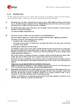
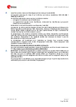
Page 130: ...minimum distance of 20 cm between the radiator and the body of the user or nearby persons This transmitter must not be co located or operating in conjunction with any other antenna or transmitter exce...

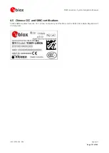
Page 131: ...em Integration Manual UBX 16024839 R04 Approvals Page 131 of 143 4 5 Chinese CCC and SRRC certifications TOBY L4906 modules have the CCC China Compulsory Certification and the SRRC State Radio Regulat...

Page 132: ...ical automatic test equipment ATE in a production line The following typical tests are among the production tests Digital self test firmware download Flash firmware verification IMEI programming Measu...

Page 133: ...RF performance tests see the following section 5 2 2 for details 5 2 1 Go No go tests for integrated devices A Go No go test is typically performed to compare the signal quality with a Golden Device...

Page 134: ...ring LTE 3G 2G signaling protocol This emission can generate interference that can be prohibited by law in some countries The use of this feature is intended for testing purposes in controlled environ...

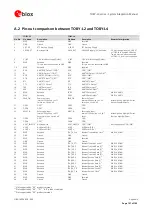
Page 135: ...1 RSVD 21 GPIO1 19 RSVD 18 RSVD 16 TXD 15 CTS 13 DTR 12 DCD 29 ETH _TX_CLK 27 USB_D 26 H OST_SELECT0 24 GPIO3 23 RESET_N 8 RSVD 6 RSVD 3 V_BCKP 22 GPIO2 20 PWR_ON 17 RXD 14 RTS 28 USB_D 25 GPIO4 9 RSV...

Page 136: ...00 950 750 700 800 850 900 950 750 960 700 703 5 5 13 13 12 12 29 V V VIII VIII 850 850 900 900 20 20 8 8 28 28 5 5 8 8 V VIII VIII V 850 900 850 900 VIII VIII 3 3 1 1 7 7 I I II II 3 3 7 7 I I 1 1 3...

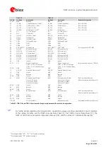
Page 137: ...p slightly different No functional difference 21 GPIO1 GPIO 23 GPIO1 GPIO 22 GPIO2 GPIO 23 GPIO2 GPIO 23 RESET_N Reset signal Input Internal 50k pull up to VCC Reset Switch on Switch off RESET_N Reset...

Page 138: ...ta 1 26 69 GND Ground GND Ground 70 72 VCC Module Supply Input 3 40 V 4 35 V normal range 3 20 V 4 35 V extended range VCC Module Supply Input 3 40 V 4 40 V normal range 3 00 V 4 50 V extended range L...

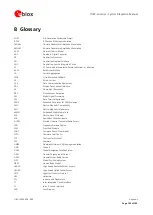
Page 139: ...gital Signal Processing DTE Data Terminal Equipment EDGE Enhanced Data rates for GSM Evolution EMC Electro Magnetic Compatibility EMI Electro Magnetic Interference eMMC Embedded Multi Media Card ESD E...

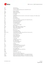
Page 140: ...TC Real Time Clock SAW Surface Acoustic Wave SDIO Secure Digital Input Output SDN PCN IN Sample Delivery Note Product Change Notification Information Note SIM Subscriber Identification Module SMS Shor...

Page 141: ...loads TS 09_v10 0 pdf 11 3GPP TS 51 010 2 Technical Specification Group GSM EDGE Radio Access Network Mobile Station MS conformance specification Part 2 Protocol Implementation Conformance Statement P...

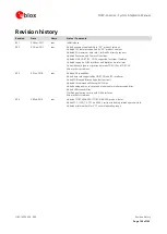
Page 142: ...M interfaces and digital audio interfaces Corrected some typo in migration between TOBY L2 and TOBY L4 Minor other corrections R03 03 Jan 2018 sses Added USB capabilities Added data rate supported by...

Page 143: ...x com Regional Office China Beijing Phone 86 10 68 133 545 E mail info_cn u blox com Support support_cn u blox com Regional Office China Chongqing Phone 86 23 6815 1588 E mail info_cn u blox com Suppo...

Reviews: