


LILY-W1 series - System integration manual
UBX-15027600 - R09
Design-in
Page 24 of 64
C1 - Public
2.4
Data communication interfaces
2.4.1
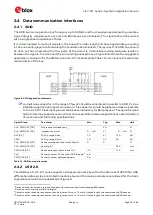
SDIO
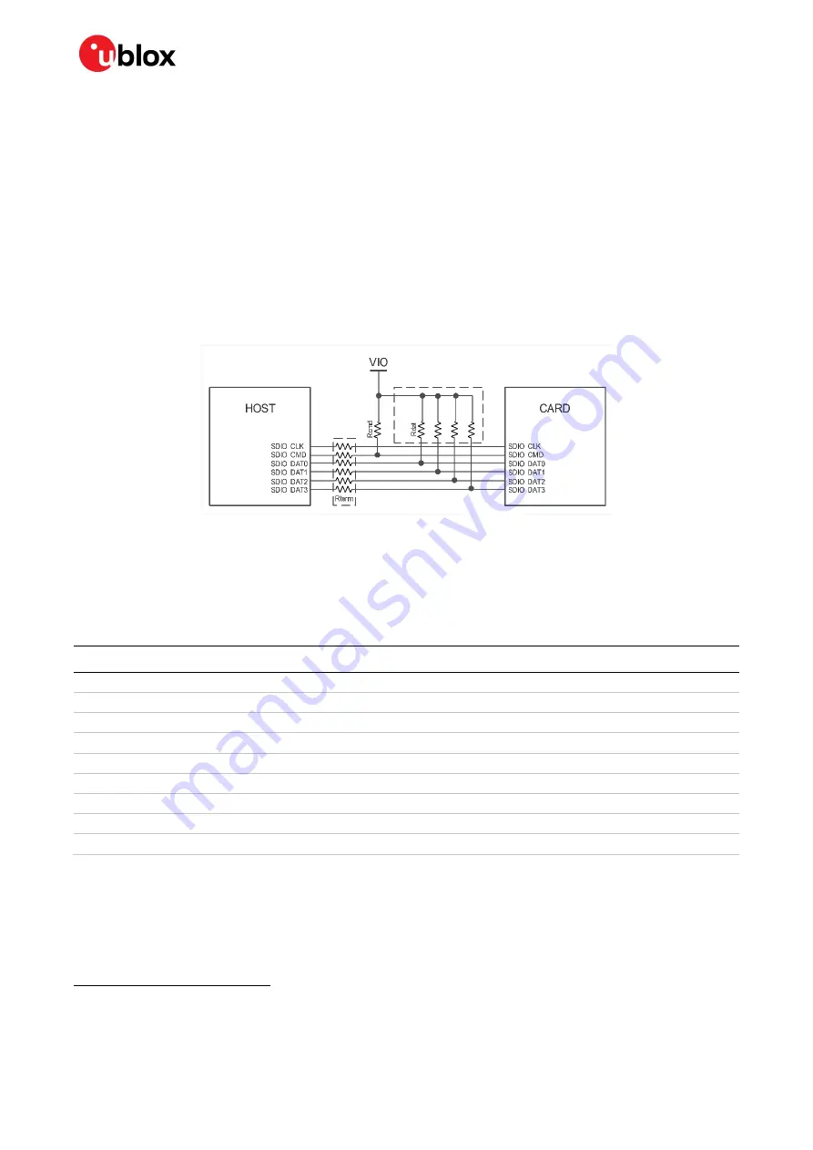
The SDIO bus can support a clock frequency up to 50 MHz and thus requires special care to guarantee
signal integrity requirements are met and EMI issues are minimized. The signals should be routed
with a single ended impedance of 50
Ω
.
It is recommended to route all signals in the bus with similar length and have appropriate grounding
in the surrounding layers; total bus length should also be minimized. The layout of the SDIO bus should
be done so that crosstalk with other parts of the circuit is minimized providing adequate isolation
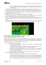
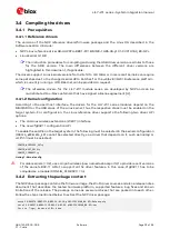
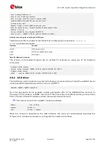
between the signals, the clock and the surrounding busses/traces. Figure 8 illustrates the suggested
application schematic for the SDIO bus in LILY-W1 modules while Table 15 summarizes the electrical
requirements of the bus.
Figure 8: SDIO application schematic
☞
A small value capacitor in the range of few pF should be considered in parallel to SDIO_CLK as
EMI debug option and signal termination. This capacitor should be placed as close as possible
to the LILY-W1 clock input pin and can be assembled only for EMI purpose. The capacitor value
adds to total line capacitance and must not exceed total allowed capacitance to avoid violation
of clock rise and fall timing specifications.
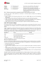
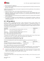
Signal Group
Parameter
Min.
Typ.
Max.
Unit
CLK, CMD, DAT[0:3]
Single ended impedance,
𝑍𝑍
0
50
Ω
CLK, CMD, DAT[0:3]
Impedance control
𝑍𝑍
0
−
10%
𝑍𝑍
0
𝑍𝑍
0
+ 10%
Ω
DAT[0:3]
Pull-Up range, Rdat
10
47
100
k
Ω
CMD
Pull-Up range, Rcmd
10
10
50
k
Ω
CLK, CMD, DAT[0:3]
Series termination (Host side), Rterm
0
0
Ω
CLK, CMD, DAT[0:3]
Bus length
200
mm
CMD, DAT[0:3]
Bus skew length mismatch to CLK
-15
+15
mm
CLK
Center to center CLK to other SDIO signals
4 w
CMD, DAT[0:3]
Center to center between signals
3 w
Table 15: SDIO bus requirements
2.4.2
USB 2.0
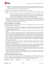
The USB bus of LILY-W1 series supports Hi-Speed connectivity with a transfer rate of 480 Mb/s. USB
differential data pair is a controlled impedance bus and the main parameters considered for the track
impedance calculation are depicted in Figure 9.
6
Series termination values larger than typical only recommended for addressing EMI issues.
7
Routing should minimize total bus length.
8
Center to center spacing requirement can be ignored for up to 10 mm of routed length to accommodate BGA escape.
9
Center to center spacing requirement can be ignored for up to 10 mm of routed length to accommodate BGA escape.