background image

DISASSEMBLY INSTRUCTIONS

B2-4

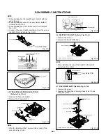
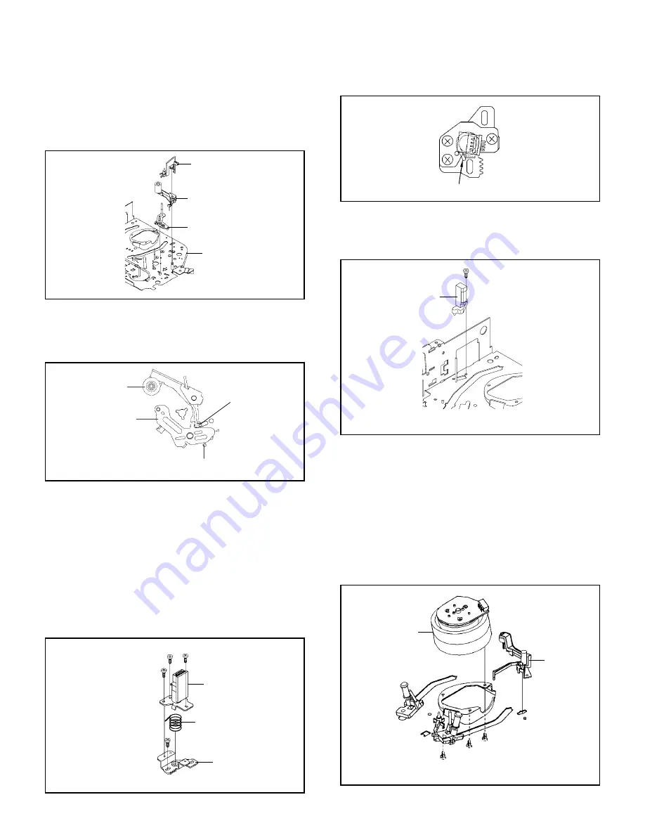
2-10: CASSETTE OPENER/PINCH ROLLER BLOCK/P5

ARM ASS’Y (Refer to Fig. 2-10-A)

1.
2.

Unlock the support 

1

 and remove the Cassette Opener.

Remove the Pinch Roller Block and P5 Arm Ass’y.

Fig. 2-10-A

Cassette Opener

1

Pinch Roller Block

P5 Arm Ass’y

Main Chassis

NOTE

1.
2.

Do not touch the Pinch Roller. (Use gloves.)
In case of the Pinch Roller Block and the Pinch Roller
Cam installation, install correctly as Fig. 2-10-B.

Fig. 2-10-B

Pinch Roller Block

Can be seen the hole of
the Pinch Roller Cam.

P5 Arm Ass’y

Can be seen the hole of the
Main Cam.

2-11: A/C HEAD (Refer to Fig. 2-11-A)

1.
2.
3.
4.

Remove the screw 

1

.

Remove the A/C Head Base.
Remove the 3 screws 

2

.

Remove the A/C Head and A/C Head Spring.

NOTE

1.
2.

3.

Do not touch the A/C Head. (Use gloves.)
When you install the A/C Head Spring, install as shown in
Fig. 2-11-B.
When you install the A/C Head, tighten the screw (1) first,
then tighten the screw (2), finally tighten the screw (3).

Fig. 2-11-A

(1)

2

A/C Head

A/C Head Spring

A/C Head Base

• Screw Torque: 5 

±

 0.5kgf•cm (Screw 

1

)

2

2

(3)

(2)

1

Fig. 2-11-B

Spring Position

2-12: FE HEAD (RECORDER ONLY) (Refer to Fig. 2-12)

1.
2.

Remove the screw 

1

.

Remove the FE Head.

Fig. 2-12

1

FE Head

• Screw Torque: 5 

±

 0.5kgf•cm

• The FE Head is not installed on the Video Cassette Player.

2-13: AHC ASS'Y/CYLINDER UNIT ASS'Y

(Refer to Fig. 2-13)

Unlock the support 

1

 and remove the AHC Ass'y.

Disconnect the following connector: (CD2001)
Remove the 3 screws 

2

.

Remove the Cylinder Unit Ass'y.

1.
2.
3.
4.

When you install the Cylinder Unit Ass'y, tighten the
screws from (1) to (3) in order while pulling the Ass'y
toward the left front direction.

NOTE

Fig. 2-13

1.

Cylinder Unit Ass'y

2

2

2

• Screw Torque: 3 

±

 0.5kgf•cm

(1)

(3)

(2)

AHC Ass'y

1

Summary of Contents for MW27FP1C

Page 1: ...SERVICE MANUAL COLOR TELEVISION VIDEO CASSETTE RECORDER DVD VIDEO PLAYER MW27FP1C FILE NO 140 200420 ...

Page 2: ... a ground conductive wrist strap for body Location of the required Marking The rating sheet and the safety caution are on the rear of the unit CERTIFICATION COMPLIES WITH FDA RADIATION PERFORMANCE STANDARDS 21 CFR SUBCHAPTER J CAUTION THIS DIGITAL VIDEO PLAYER EMPLOYS A LASER SYSTEM TO ENSURE PROPER USE OF THIS PRODUCT PLEASE READ THIS SERVICE MANUAL CARE FULLY AND RETAIN FOR FUTURE REFERENCE SHOU...

Page 3: ...itions or whether there are the portions which are deteriorated around the serviced places serviced or not Check the insulation between the antenna terminal or external metal and the AC cord plug blades And be sure the safety of that INSULATION CHECK PROCEDURE 1 2 3 4 Unplug the plug from the AC outlet Remove the antenna terminal on TV and turn on the TV Insulation resistance between the cord plug...

Page 4: ...al power company For units intended to operate from battery power or other sources refer to the operating instructions GROUNDING OR POLARIZATION This unit is equipped with a polarized alternating current line plug a plug having one blade wider than the other This plug will fit into the power outlet only one way This is a safety feature If you are unable to insert the plug fully into the outlet try...

Page 5: ...r equipment turn off the power and unplug all of the equipment from the wall outlet Failure to do so may cause an electric shock and serious personal injury Read the owner s manual of the other equipment carefully and follow the instructions when making any connections SOUND VOLUME Reduce the volume to the minimum level before you turn on the product Otherwise sudden high volume sound may cause he...

Page 6: ...A DISCHARGE UNIT NEC SECTION 810 20 ANTENNA LEAD IN WIRE GROUNDING CONDUCTORS NEC SECTION 810 21 GROUND CLAMPS POWER SERVICE GROUNDING ELECTRODE SYSTEM NEC ART 250 PART H GROUND CLAMP ELECTRIC SERVICE EQUIPMENT NEC NATIONAL ELECTRICAL CODE S2898A IMPORTANT SAFEGUARDS CONTINUED ...

Page 7: ...sette Case Repeat the above step 3 4 Then take out the Video Cassette from the Deck Chassis Be careful not to scratch on the tape TAPE REMOVAL METHOD AT NO POWER SUPPLY Fig 1 Pinch Roller Cam Main Cam Clutch Ass y Main Chassis Front Side Loading Motor Screw 1 Capstan DD Unit Fig 2 1 2 3 Remove the Back Cabinet TV DVD VCR Block and DVD TOP Refer to item 1 of the DISASSEMBLY INSTRUCTIONS Slide the R...

Page 8: ...et the VOLUME to minimum Press and hold the REC OTR button on the front panel Simultaneously press and hold the 4 key on the remote control unit Hold both keys for more than 2 second The On Screen Display message INITIALIZE5 COMPLETE will appear The Tray Lock has now been cleared 1 2 3 4 5 6 7 8 If the stored 4 digit password in the Rating Level menu needs to be cancelled please follow the steps b...

Page 9: ...ICAL PARTS AND P C BOARDS 2 REMOVAL OF VCR DECK PARTS 3 REMOVAL OF DVD DECK PARTS 4 REMOVAL OF ANODE CAP 5 REMOVAL AND INSTALLATION OF FLAT PACKAGE IC KEY TO ABBREVIATIONS SERVICE MODE LIST PREVENTIVE CHECKS AND SERVICE INTERVALS WHEN REPLACING EEPROM MEMORY IC SERVICING FIXTURES AND TOOLS PREPARATION FOR SERVICING MECHANICAL ADJUSTMENTS ELECTRICAL ADJUSTMENTS BLOCK DIAGRAMS DVD Y C AUDIO HEAD AMP...

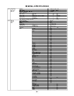
Page 10: ...SLP EP 3x 5x 9x 15x Picture Search Frame Advance Yes Slow Speed 1 10 G 3 DVD System Color System NTSC Disc DVD CD DA CD R RW Video CD Disc Diameter 120 mm 80 mm Deck Disc Loading System Front Loading Motor 2 Motors Pick up 1 Lens 2 Beams System Playback time Max DVD 1 Layer 135min 4 7GB DVD 2 Layer 245min 8 5GB CD 74min Video CD 74min Search speed Fwd 2 20 times 4 step Actual 2 45 times DVD VIDEO ...

Page 11: ...ode 0 06 1kHz Harmonic Distortion at VCR SP Mode 1 5 1kHz Typical Frequency Response DVD Mode at DVD 4Hz 22kHz at Video CD 4Hz 20kHz at SVCD at CD 4Hz 20kHz VCR Mode at SP 100Hz 10kHz at LP at SLP 100Hz 4kHz Hi Fi Audio Signal Dynamic Range More than 90 dB Frequency Response 20Hz 20kHz Wow And Flutter Less than 0 01 Wrms Channel Separation More than 60 dB Harmonic Distortion Less than 1 0 G 6 Powe...

Page 12: ...Setup Yes Timer Rec Set Yes Auto Repeat On Off Yes G CODE or SHOWVIEW or PLUSCODE No Entry No Clock Date Yes TV VCR Yes DVD Yes CH AV LINE Yes Tape Counter Linear Counter Yes Tape Speed Yes Sleep Time Yes Stereo Audio Output Yes Bilingual No SAP Yes Control Volume Yes Level Brightness Contrast Sharpness Color Yes Tint Yes Bass Treble Balance Yes Manual Tracking Yes Play Stop FF Rew Rec OTR T Rec P...

Page 13: ...GB Composite No Open Yes Close Yes No disc Yes Reading Yes Play Yes Still Pause Yes Stop Yes Prohibit Mark Yes Step Yes Skip Yes Skip Yes Random Yes CD VIDEO CD MP3 WMA JPEG Repeat Yes Slow Yes Slow No Search Yes Search Yes Jump Yes Resume Yes Title No Yes Chapter No Yes Track No Yes Time Yes Sub Title No Yes Angle No Yes Vocal On Off Yes Audio No Yes Audio Stereo L R Yes Video CD Zoom Yes Marker ...

Page 14: ...ys TV VCR Yes DVD Yes Power Yes 1 Yes 2 Yes 3 Yes 4 Yes 5 Yes 6 Yes 7 Yes 8 Yes 9 Yes 0 Yes Channel Yes Channel Yes Volume Yes Volume Yes Display Yes Sleep Yes Audio Select Yes Mute Yes Channel Return Skip Yes Closed Caption Skip Yes T REC Yes Rec T Rec OTR Yes Rec OTR Yes Slow Yes Play Yes Stop Yes Rew Yes F Fwd Yes Pause Still Yes CM Skip Jump Yes SP SLP Return Yes Counter Reset Angle Yes Zero R...

Page 15: ...TV Monitor No Program Extend No Choke Coil No Energy Star Yes Protect of FBT Leak Circuit Yes Zero Return Yes Power On Memory No Dirty Head No V chip USA V chip No CANADA V chip No Parental Lock DVD Only Yes Tray Lock Yes Auto Stop Pause and Resume Stop after 5min Yes Video CD Playback Yes SVCD Playback No Overlay Graphics And Text No Command List No Entry Point Jump No MP3 Playback Yes WMA Playba...

Page 16: ... No G 17 Interface Switch Front Power Tact Yes Channel Up Yes Channel Down Yes Volume Up Yes Volume Down Yes Play VCR Yes Stop Eject VCR Yes F FWD Cue VCR Yes Rew Rev VCR Yes REC OTR VCR Yes Play DVD Yes Stop DVD Yes Skip Search DVD Yes Skip Search DVD Yes Open Close DVD Yes Input Select No Main Power SW No Indicator Power Yes Red REC OTR Yes Red T REC Yes Red TV VCR No DVD No Terminals Front Vide...

Page 17: ... mm 851 x 618 x 776 Design As per Buyer s Description of Origin Yes Drop Test Natural Dropping At 1 Corner 3 Edges 6 Surfaces Height cm 25 Container Stuffing 40 container 156 Sets G 21 Material Cabinet Front PS 94V0 DECABROM Rear PS 94V0 DECABROM Jack Panel PCB Non Halogen Demand No Eyelet Demand Yes G 22 Environment Pb Free Lead free Solder No Other No Cd Free No A3 8 ...

Page 18: ...ack Cabinet 1 1 2 2 1 3 TV DVD VCR BLOCK Refer to Fig 1 3 1 2 3 Remove the 2 screws 1 Disconnect the following connectors CP303 CP404 and CP1704 Remove the TV DVD VCR Block in the direction of arrow Fig 1 3 1 4 VCR DECK Refer to Fig 1 4 NOTE Do not remove the cable at the FE Head section The FE Head may be damaged if you remove the cable by force 1 2 3 4 5 6 7 8 9 10 11 12 Remove the 2 screws 1 Re...

Page 19: ... 4 screws 3 Remove the DVD PCB in the direction of arrow C NOTE When the installation of the DVD Deck remove all the soldering on the short circuit position after the connection of Pick Up PCB and DVD PCB connector DVD Block 2 DVD Shield 2 2 2 1 1 A 3 3 B Operation PCB Bottom Plate 1 8 DEFLECTION PCB Refer to Fig 1 8 1 2 3 Remove the 2 screws 1 Remove the 3 screws 2 Remove the Deflection PCB in th...

Page 20: ...ve the Locker Spring Unlock the 4 supports 1 and then remove the Cassette Side L R Unlock the support 2 and then remove the Locker R Locker Spring Cassette Side L Cassette Side R Locker R Cassette Holder 1 1 1 1 2 In case of the Locker R installation check if the one position of Fig 2 3 B are correctly locked When you install the Cassette Side R be sure to move the Locker R after installing NOTE 1...

Page 21: ...ension Connect Tension Spring Tension Arm Ass y Tension Holder 1 1 3 2 4 NOTE 1 2 3 In case of the Tension Band installation note the direc tion of the installation Refer to Fig 2 7 C In case of the Tension Band installation install correctly as Fig 2 7 D In case of the Tension Connect installation install as the circled section of Fig 2 7 E Fig 2 7 C Tension Band Tension Connect Tension Arm Ass y...

Page 22: ...NOTE 1 2 3 4 5 6 Take care not to damage the gears of the S Reel and T Reel The Polyslider Washer may be remained on the back of the reel Take care not to damage the shaft Do not touch the section A of S Reel and T Reel Use gloves Refer to Fig 2 9 A Do not adhere the stains on it When you install the reel clean the shaft and grease it If you do not grease noise may be heard in FF REW mode After in...

Page 23: ...e A C Head Use gloves When you install the A C Head Spring install as shown in Fig 2 11 B When you install the A C Head tighten the screw 1 first then tighten the screw 2 finally tighten the screw 3 Fig 2 11 A 1 2 A C Head A C Head Spring A C Head Base Screw Torque 5 0 5kgf cm Screw 1 2 2 3 2 1 Fig 2 11 B Spring Position 2 12 FE HEAD RECORDER ONLY Refer to Fig 2 12 1 2 Remove the screw 1 Remove th...

Page 24: ...2 15 B And also can be seen the Main Chassis hole through the Main Cam maker hole Fig 2 15 B Pinch Roller Cam Marker Main Cam 2 16 LOADING GEAR S T UNIT Refer to Fig 2 16 A 1 2 Remove the E Ring 1 and remove the Main Loading Gear Remove the Main Rod Tension Lever Loading Arm S Unit and Loading Arm T Unit 1 Main Loading Gear Main Rod Tension Lever Loading Arm T Unit Loading Arm S Unit Fig 2 16 A NO...

Page 25: ... inserting the spring of the Clutch Ass y into the dent of the Coupling Gear Refer to Fig 2 17 B Fig 2 17 B Clutch Ass y Coupling Gear 2 18 CASSETTE GUIDE POST INCLINED BASE S T UNIT P4 CAP Refer to Fig 2 18 A 1 2 3 4 5 Remove the P4 Cap Unlock the support 1 and remove the Cassette Guide Post Remove the Inclined Base S T Unit Remove the screw 2 Remove the LED Reflector Fig 2 18 A NOTE 1 2 3 Do not...

Page 26: ...r R Green 1 Main Frame Ass y Main Chassis Ass y 3 4 CLAMPER ASS Y INSULATOR R LEVER SWITCH Refer to Fig 3 4 A 1 2 3 4 5 Remove the screw 1 Remove the Lever Switch Remove the 2 Insulator R Press the Clamper and rotate the Clamper Plate clockwise then unlock the 3 supports 2 Remove the Clamper Plate Clamper Magnet and Clamper Insulator R Green Insulator R Green Clamper Plate Clamper Magnet Main Fram...

Page 27: ... D Fig 3 4 B Fig 3 4 C Fig 3 4 D 3 5 TRAVERSE HOLDER INSULATOR F Refer to Fig 3 5 A 1 2 Remove the Traverse Holder Remove the 2 Insulator F Main Chassis Ass y Insulator F Black Traverse Holder Insulator F Black Fig 3 5 A Lever Switch Blue White Red From DVD PCB NOTE 1 After the installing of the Traverse Holder check if the wire is like Fig 3 5 B 3 6 SWITCH PCB ASS Y Refer to Fig 3 6 A Remove the ...

Page 28: ...k if the Rack Feed 1 2 is moving smoothly Refer to Fig 3 7 B In case of the Rack Feed Ass y installation install cor rectly as Fig 3 7 C Moving smoothly Moving smoothly Fig 3 7 B Should not be engaged Check the position of the Rack Feed Lever Fig 3 7 C 3 8 RELAY PCB ASS Y Refer to Fig 3 8 A 1 2 Remove the screw 1 Remove the Relay PCB Ass y Main Chassis Ass y Relay PCB Ass y Screw Torque 4 0 5kgf c...

Page 29: ... 1 1 Motor Gear Feed Motor Main Chassis Ass y NOTE 1 2 In case of the Motor Gear installation check if the value of the Fig 3 11 B is correct When installing the Feed Motor check if the cable is positioned as Fig 3 11 C Fig 3 11 B 6 1 0 1mm Safety surface for pressing of the insert Feed Motor Motor Gear Fig 3 11 C Main Chassis Ass y Feed Motor Pass the cable between 2 pins ...

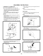
Page 30: ...ip up the sides of the Rubber Cap in the direction of the arrow and remove one side of the support Refer to Fig 4 2 2 GND on the CRT Screwdriver Alligator Clip Support CRT GND on the CRT Rubber Cap CRT Support Fig 4 1 Fig 4 2 3 After one side is removed pull in the opposite direction to remove the other NOTE DISASSEMBLY INSTRUCTIONS INSTALLATION 1 Clean the spot where the cap was located with a sm...

Page 31: ...ring the IC leads completely Fig 5 2 Blower type IC desoldering machine IC 3 When IC starts moving back and forth easily after desoldering completely pickup the corner of the IC using a tweezers and remove the IC by moving with the IC desoldering machine Refer to Fig 5 3 NOTE Some ICs on the PCB are affixed with glue so be careful not to break or damage the foil of each IC leads or solder lands un...

Page 32: ...eld Wire Refer to Fig 5 7 NOTE Do not absorb the solder to excess Fig 5 7 Soldering Iron IC Braided Shield Wire 4 When bridge soldering between terminals and or the soldering amount are not enough resolder using a Thin tip Soldering Iron Refer to Fig 5 8 Fig 5 8 Thin tip Soldering Iron IC 5 Finally confirm the soldering status on four sides of the IC using a magnifying glass Confirm that no abnorm...

Page 33: ...Flip flop Frequency Generator Front Loading Switch Frequency Modulation Frequency Sub Carrier Forward Generator Ground H I K L M N O P R S H P F H SW Hz IC IF IND INV KIL L LED LIMIT AMP LM LDM LP L P F LUMI M MAX MINI MIX MM MOD MPX MS SW NC NR OSC OPE PB PB CTL PB C PB Y PCB P CON PD PG P P R REC REC C REC Y REEL BRK REEL S REF REG REW REV RVS RF RMC RY S CLK S COM S DATA SEG SEL SENS SER SI SIF...

Page 34: ...on Sync Separator Separation Transistor Tracking Trick Playback Test Point Unregulated Volt Voltage Controlled Oscillator Video Intermediate Frequency Vertical Pulse Voltage Display Video Playback Variable Resistor Video Recording Visual Search Fast Forward Visual Search Rewind Voltage Super Source Vertical Synchronization Voltage Tuning Crystal Luminance Chrominance C1 2 ...

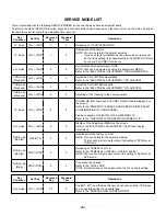
Page 35: ...ER Adjust the PG SHIFTER manually Refer to the ELECTRICAL ADJUSTMENT PG SHIFTER Adjusting of the Tracking to the center position POWER ON total hours and PLAY REC total hours are displayed on the screen Refer to the PREVENTIVE CHECKS AND SERVICE INTERVALS CONFIRMATION OF HOURS USED Can be checked of the INITIAL DATA of MEMORY IC Refer to the WHEN REPLACING EEPROM MEMORY IC Display of the Adjustmen...

Page 36: ... parts in contact with the tape Clean the rubber and parts which the rubber touches Replace when rolling becomes abnormal Clean the Head T Brake Band Clutch Ass y Idler Arm Ass y CONFIRMATION OF HOURS USED POWER ON total hours and PLAY REC total hours can be checked on the screen Total hours are displayed in 16 system of notation NOTE If you set a factory initialization the total hours is reset to...

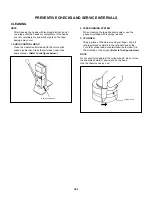
Page 37: ... in the same manner Refer to the figure below 2 TAPE RUNNING SYSTEM When cleaning the tape transport system use the gauze moistened with isopropyl alcohol 3 CYLINDER Wrap a piece of chamois around your finger Dip it in isopropyl alcohol Hold it to the cylinder head softly Turn the cylinder head counterclockwise to clean it in the direction of the arrow Refer to the figure below NOTE Do not exert f...

Page 38: ...cessary Repeat steps 4 to 7 until all data has been checked When satisfied correct DATA has been entered turn POWER off return to STANDBY MODE to finish DATA input After the data input set to the initializing of shipping Turn POWER on Press both VOL DOWN button on the set and the Channel button 1 on the remote control for more than 2 seconds After the finishing of the initializing of shipping the ...

Page 39: ...S Reel T Reel Ass y Brake Torque T Reel Ass y VSR Torque Brake Torque S Reel APJG022000 JG022 Master Plane Reel Disk Height Adjustment JG024A APJG024A00 Reel Disk Height Adjustment Jig Reel Disk Height Adjustment JG153 APJG153000 X Value Adjustment Screwdriver X Value Adjustment PREPARATION FOR SERVICING 1 2 3 Set the VOLUME to minimum Press both VOL DOWN button on the set and the FF button on the...

Page 40: ...es 20 2gf in the beginning of playback 1 2 USING A CASSETTE TYPE TORQUE TAPE KT 300NR 1 2 3 After confirmation and adjustment of Tension Post position Refer to item 1 2 load the cassette type torque tape KT 300NR and set to the PLAY mode Confirm that the right meter of the torque tape indicates 50 90gf cm during playback in SP mode Confirm that the left meter of the torque tape indicates 25 40gf c...

Page 41: ...1 B even if you press the Tracking Button to move the envelope The envelope waveform will begin to decrease when you press the Tracking Button Adjust the PG shifter during playback Refer to the ELECTRICAL ADJUSTMENTS 1 2 3 4 5 6 7 NOTE After adjustment confirm and adjust A C head Refer to item 2 2 CH 2 SW Pulse TP102 CH 1 Track CH 2 Track CH 1 Envelope TP4501 Fig 2 1 A Fig 2 1 B NOTE Install the T...

Page 42: ...then adjust the a P4 Cap Fig 2 2 A Audio Control Head 1 3 2 Fig 2 2 B Audio Control Head Fig 2 2 C TAPE RUNNING ADJUSTMENT X VALUE ADJUSTMENT Confirm and adjust the height of the Reel Disk Refer to item 1 1 Confirm and adjust the position of the Tension Post Refer to item 1 2 Adjust the Guide Roller Refer to item 2 1 Confirm and adjust the Audio Control Head Refer to item 2 2 Connect CH 1 of the o...

Page 43: ...USTMENT PARTS LOCATION GUIDE 5 6 7 8 9 10 1 2 3 4 1 Tension Connect 2 Tension Arm 3 Guide Roller 4 Audio Control Head 5 X value adjustment driver hole 6 7 8 9 10 P4 Post T Brake Spring T Reel S Reel Adjusting section for the Tension Arm position ...

Page 44: ...racking button until the arising to the down of Head Switching Pulse becomes 6 5 0 5H Refer to Fig 2 1 A B Fig 2 1 B Fig 2 1 A 2 BASIC ADJUSTMENTS 6 5H CH 1 CH 2 6 5H CH 2 CH 1 1 Read and perform these adjustments when repairing the circuits or replacing electrical parts or PCB assemblies CAUTION Use an isolation transformer when performing any service on this chassis Before removing the anode cap...

Page 45: ...FT quantity of the OVER SCAN on right and left becomes minimum 2 9 VERTICAL SIZE 1 2 3 4 Receive the monoscope pattern Using the remote control set the brightness and contrast to normal position Activate the adjustment mode display of Fig 1 1 and press the channel button 06 on the remote control to select V SIZE Press the VOL UP DOWN button on the remote control until the Up Down OVER SCAN Quantit...

Page 46: ...te control to set to the DVD mode Activate the adjustment mode display of Fig 1 1 and press the channel button 17 on the remote control to select BRI CENT Press the VOL UP DOWN button on the remote control to up the step numbers by 5 steps to the AV mode A 2 15 OSD HORIZONTAL Activate the adjustment mode display of Fig 1 1 Press the VOL UP DOWN button on the remote control until the difference of ...

Page 47: ...Fig 1 1 and press the channel button 21 on the remote control to select CONT MAX Press the VOL UP DOWN button on the remote control to set the same step numbers as the AV mode 1 2 3 4 5 6 7 8 9 10 11 2 18 COLOR CENTER Receive the color bar pattern RF Input Using the remote control set the brightness contrast color and tint to normal position Connect the oscilloscope to TP804 Activate the adjustmen...

Page 48: ...s between the deflection yoke and CRT funnel to fix the deflection yoke Refer to Fig 3 2 b R G B R G B Fig 3 2 a WEDGE WEDGE WEDGE WEDGE POSITION Fig 3 2 b R G B R G B Receive the crosshatch pattern from the color bar generator Combine red and blue of the 3 color crosshatch pattern on the center of the screen by adjusting the pair of 4 pole magnets Combine red blue magenta and green by adjusting t...

Page 49: ...2301 CD2001 CD2302 CP8502 CD8505 CP2601 CP2603 CP2602 CD2251 CP8001 CP602 CP1702 CP4502 AC HEAD CD4501 CD603 TP4501 TP102 J2204 J2203 J2202 J2201 DVD DECK DVD DECK TP401 VCR DECK CP404 CRT FB401 CP802A VR404 CP604 CP602B CP303 SPEAKER CD303 CP4503 FE HEAD VR1701 CP601 TU001 AC IN CD1702 CP1704 J8007 J4202 J4201 TP4201 CP001 CRT DEFLECTION PCB VCR PCB CD002 CD604 CD602 CD8501 CP851A CP804 CD851 TP8...

Page 50: ... TV BLOCK TX RX P CON 3 3V DVD BLOCK DIAGRAM CD DVD LD RFA_SDEN DATA SCLK EEPROM IC4002 S 24C04BFJ TB RF AAF_CE FE TE PI FNN FNP VBIASS0 S1 DEFECT LINK MIRR LDON HOME TIN SW TOUT SW TR FO SPDL SLED SPINDLE SLED_PWM TRACK FOCUS_DAC ADC IN 5 6 7 S MUTE HA0 HA20 HD0 HD15 SD D0 D15 I2CDAT P CON 5V P CON 9V DVD RESET DVD_A_OUT_L DVD_A_OUT_R ZERO ASDATA0 AMCLK ABCLK ALRCLK SD A0 A11 BA0 RAM CS0 CSI RAS ...

Page 51: ...VCA CLAMP 1 2 FBC Chara INS 6dB P R P R V AGC L4502 CLAMP EQ AMP LINE AMP MUTE ALC Y C_CS Y C_DATA Y C_CLK H AMP_SW1 C ROTARY H SW ENV DET COMP DUMMY_V SYNC AUX_V F R TUNER_VIDEO NORMAL_A Y C_AUDIO 6 2 3 1 5 Q4505 BIAS CTL 11 4 H AMP SW AUDIO MUTE C ROT RF SW IN ENV DET COMP OUT Q4504 BIAS OSC Q4503 SW Q4501 Q4502 AUDIO PB SW HF1 HF2 HI FI DEMODULATOR HF_COM COIL BIAS OSC X4501 3 579545MHz VX01 50...

Page 52: ...C IC199 AT24C04N 10SI 2 7 Y C DATA 13 Y C CLK 11 Y C_DATA Y C_CLK CVN2 50 Y C VIDEO SCL SDA COMP 100 COMP REC OTR LED EXT_A_MUTE 91 9 EXT_MUTE 6 REC_LED EXT_A_MUTE EXT_MUTE ST SELECT 87 HIFI H SW 26 HIFI ENV 88 ST_SELECT HIFI_H SW HIFI_ENV SDA SCL VCR_A_MUTE V REC_ST_H HI FI DEMODULATOR VCR_POWER_ON H 92 VCR_POWER_H EMERGENCY 86 EMERGENCY MICON BLOCK DIAGRAM RX 15 TX X101 32 768KHz X0 XI 40 41 TX ...

Page 53: ...R_H T REC_LED REC_LED VCR_A_MUTE MUTE SW CH MUTE MUTE SW REAR OUT JACK J4202 HEADPHONE JACK J2201 SOUND_L SP_OUT_R SP_OUT_L Q4210 MUTE SW EXT_MUTE JACK_OUT REAR IN JACK J4201 FRONT_V_IN REAR_A_IN_L REAR_A_IN_R REAR_V_IN FRONT VIDEO JACK J2202 FRONT_A_IN_L FRONT AUDIO L JACK J2203 FRONT_A_IN_R FRONT AUDIO R JACK J2204 MICON SOUND AMP SURROUND DIGITAL COMB FILTER HI FI DEMODULATOR 3 ZERO SW Q4204 D ...

Page 54: ... 3 1 OSD_Y OSD_R OSD_B OSD_G SCL V_SYNC SDA H SYNC SW_C COMB FSC Y C_VIDEO_Y DVD_Y C_Y V_SYNC DIGITAL COMB FILTER DVD IN OUT Q602 PROTECT G OUT CUT OFF FROM TO CRT SVM CP802 6 5 4 VM_OUT CLAMP OFF B OUT 3 1 R OUT VM_OSD_Y 7 8 ACL V OUT FROM TO DEFLECTION CP602 6 5 4 P CON 5V H OUT EW OUT 3 2 1 AFC TV_POWER_H EMERGENCY 7 8 9 B DOWN TV_POWER_H EMERGENCY MICON Q606 SW PROTECT MICON Y C AUDIO HEAD AMP...

Page 55: ...R SP_OUT_L SOUND AMP SURROUND BLOCK DIAGRAM SPEAKER SP352 SPEAKER SP351 TV_POWER_H SCL TV_A_MUTE SDA P CON 8V 30 18 17 31 SURROUND IC IC302 AN5891SA E1V 19 3 16 SW_AUDIO_OUT_L SW_AUDIO_OUT_R SW_AUDIO_OUT_R SW_AUDIO_OUT_L MICON REGULATOR IN OUT DVD IN OUT 1 SOUND B TV E 11 E 12 ...

Page 56: ...F_COM FSC HF1 Y C_AUDIO NORMAL_A IN OUT MICON Y C AUDIO HEAD AMP 51 58 40 P CON 12V P CON 5V_A INPUT SW AMP AMP RFC OUTPUT SW PNR BPF FM LIM DEM BLOCK AMP AMP AGC LOGIC VCO FO ADJ LOGIC 25 DBX NOISE REDUCTION L R MIX REC LPF VCO 4 2 Hi Fi DEMODULATOR BLOCK DIAGRAM 1 3 DVD_A_OUT_L DVD_A_OUT_R DVD IN OUT REGULATOR 15 10 FRONT_A_IN_R FRONT_A_IN_L AUDIO_OUT_L AUDIO_OUT_R NC DIGITAL COMB FILTER E 13 E ...

Page 57: ...01 TC90A45F 13 15 16 8 4 10 AV SW IC IC1502 MM1501XNRE 2 6 1 4 3 AV SW IC IC1504 MM1501XNRE 2 6 1 4 3 VIDEO OUT SW IC IC1505 MM1504XNRE 2 6 1 4 3 BUFFER Q1501 COMB_FSC BUFFER Q1503 P CON 5V P CON 12V BUFFER Q1502 DVD IN OUT Y C AUDIO HEAD AMP IN OUT P CON 8V 3 10 11 TU001 115 V K015AR B 12 14 15 17 SCL SDA TUNER_AUDIO HI FI DEMODULATOR TUNER VIDEO AFT AT 30V Y C AUDIO HEAD AMP E 15 E 16 ...

Page 58: ... CVBS RX P CON 9V_D P CON 5V_D P CON 3 3V SPDIF 134 DVD_RESET 2 3 5 3 MIXER IC IC8004 NJM4580M TE1 7 1 6 1 4 AUDIO SW IC IC8002 MM1501XNRE 2 3 Q8006 Q8007 ZERO MUTE SW IN OUT AUDIO_OUT_L AUDIO_OUT_R DVD_A_OUT_L DVD_A_OUT_R P CON 12V AV SW1 DVD_Y C_Y DVD_Y C_C DVD_VIDEO CHROMA IF Y C AUDIO HEAD AMP ZERO HI FI DEMODULATOR DVD_VIDEO SW_AUDIO_OUT_L SW_AUDIO_OUT_R MICON DIGITAL COMB FILTER SOUND AMP SU...

Page 59: ...002 KIA278R09PI Q3014 BACKUP 5V Q3015 BUFFER Q3001 BUFFER MOTOR 12V Q3010 P CON 5V_C SW AT 12V VCR_POWER_H P CON 5V_A DVD_H BACKUP 5V AT 5V P CON 12V P CON 8V IN OUT HI FI DEMODULATOR B Q3005 3 3V OUT Q3004 3 3V CTL Q3006 3 3V CTL Q3007 P CON 12V SW 30V DIGITAL COMB FILTER P CON 12V P CON 5V_D P CON 9V_D P CON 3 3V AT 5V P CON 5V P CON 8V 8 5V REG AT5 7V REG DVD IN OUT CHROMA IF SOUND AMP SURROUND...

Page 60: ...5 2 2 Q401 H DRIVE 2 T401 5 3 Q403 FL OUT RED AMP Q801 Q810 GREEN AMP Q802 Q811 BLUE AMP Q803 Q812 J801 11 8 6 F 7 MICON SOUND AMP REGULATOR RELAY DRIVER F1701 P CON 5V V OUT CP602B 4 3 2 ACL AFC TV_POWER_H 7 6 1 H OUT EW OUT EMERGENCY B DOWN 5 8 9 SW 7 9 7 Q407 H_VOLT_SW B G OUT CUT OFF CP802 7 6 5 VM_OUT CLAMP OFF B OUT 4 3 1 R OUT VM_OSD_Y 8 FEED BACK SWITCHING IC1702 TL431AILP 1 3 10 17 18 UNR...

Page 61: ... C4042 C4092 B4006 C4066 C4065 C4097 W874 R2651 R2650 R2652 R2653 R2649 R2626 C2642 C2616 R4022 C2647 B2602 R2621 C4013 C2303 R2304 C2306 C2301 B4007 C4095 C4039 W854 W802 C4077 C4082 W855 W860 W832 C4037 C4081 C4094 C4093 C4098 C4038 C4026 R4053 R4054 R4014 R4035 R4031 IC4002 B8502 B8503 B4005 W833 IC8502 Q8502 Q8503 Q8504 C8505 C8506 C8509 C8508 C8512 C8511 B4003 B4001 R4052 W857 C4001 C4003 C40...

Page 62: ...5 IC1701 D1718 R1717 C1713_1 C1712 D1717 R1714 Q1706 R1722 R1731 D1709 HS1701 W031 R1720 R 1 7 1 8 D1710 D1705 D1706 D1711 L1701 RY1701 FH1702 C1701 R1701 CD1703 CD1704 F1701 FH1701 T1701 W094 R1712 R5512 W030 W081 D2201 W020 R3001 Q3002 R3006 W018 L3002 CP602 W065 W286 W287 W044 W045 W039 W088 W090 W071 W072 W115 W161 C609 R613 W119 W174 W171 W175 W042 W043 W110 W111 W109 W035 C3025 B8001 C3022 W...

Page 63: ... Q2202 Q2201 Q2203 C2202 R105 C2205 C2203 R5522 R4560 Q116 R171 C8012 C8014 C121 C2207 C4579 C2209 R5523 R4506 C2213 C1532 C156 R177 W863 I C 1 0 1 C4514_1 R4523 IC8002 IC1504 Q106 C120 I C 6 0 1 R124 R4504 Q4502 Q4501 R4507 C117 C111 C616 C631 C629 C630 C627 C625 R148 R149 R150 R159 R160 R164 C628 R625 R626 C626 R624 C622 C621 R619 R617 C617 C606 R609 R610 R608 C608 C5517 C5534 C5535 C5538 C5541 ...

Page 64: ... R811 C804 R817 C806 R821 R819 C805 R812 J 8 0 1 _ 2 R862 R863 R865 R864 C857 R858 R861 R860 C855 R854 C856 R859 R856 R853 CP852 R855 W001 D807 D809 W805 CP851B CP801B D808 W811 W003 C809 W820 C808 W804 C863 C852 C862 C853 CP802B_1 W008 C876 W007 R893 R892 R891 Q863 C875 Q864 R896 C878 R894 Q803 Q801 Q802 C820 W821 W810 W809 W890 W808 W802 W807 W822 W823 W816 W815 W814 TEAA93C PRINTED CIRCUIT BOAR...

Page 65: ...W014 W012 R408 Q403 W011 C414 CP802A R441 W020 CP404_1 W013 CD2251 R2251 R2252 R2253 R2254 R2255 R2256 R2257 SW2258 SW2257 SW2256 SW2255 SW2254 SW2253 SW2252 SW2251 W007 C421 C438_2 Q408 D418 D417 D413 D414 D412 D410 D408 C443 C436 D407 D416 D402 C412 C423 R416 R410 W003 W004 Q409 Q407 R413 R442 W002 D411 W015 R439 R437 W008 W017 CP604 D404 W023 D403 R 43 6 R435 C409 R448 R404 R446 Q410 R422 R411 ...

Page 66: ... HA8 LINK HA12 TRAY_OPEN HA9 MIRR HA10 HD15 TOUT_SW LDON HA11 SMUTE HA11 TRAY_CLOSE HA12 TRACK_DAC HD7 TIN_SW HA13 FOCUS_DAC SMUTE HA14 SPINDLE_PWM HA15 HA10 SLED_PWM HA16 HD14 HA17 HA9 RESET HA18 P CON A5V HD6 HA19 P CON 3 3V HA20 HA8 VCC 9V HD0 P CON 5V HD13 HD1 ADCIN_7 HD5 HD2 ADCIN_6 HA20 HOME HOME HD3 ADCIN_5 HD4 LDON M_GND HD5 HD12 D_GND HD6 GND WR DJTDO ML HD7 HD4 DJTDI MC HD8 DUPTD1 HD9 DJ...

Page 67: ...D_D10 SD_D5 RAMCS0 HD12 HA20 RAMCS1 SD_D9 SD_D6 RAMRAS RAMCAS HD4 WR SD_BA0 RAMDQM SD_D8 SD_D7 RAMWE RESET RAMCLK HA0 HA1 HD11 RAMDQM HA2 HA3 RAMDQM RAMWE HA4 HD3 HA5 RAMCLK RAMCAS HA6 HA7 HD10 HA19 RAMRAS HA8 HA9 RAMCS1 HA10 HD2 HA18 HA11 SD_A11 SD_BA0 HA12 HA13 HD9 HA17 SD_A9 RAMCS0 HA14 HA15 SD_A8 SD_A10 HA16 HD1 HA7 HA17 SD_A7 SD_A0 HA18 HA19 HD8 HA6 SD_A6 SD_A1 HA20 HD0 SD_A5 SD_A2 HD1 HD0 HA...

Page 68: ... R2632 4 7K R2630 22K R2629 1 5K R2628 22K R2619 100 R2621 100 R2622 4 7K R2647 4 7K R2624 4 7K R2623 4 7K R2617 1K R2618 18 R2304 2 2 R2604 27K 1 R2331_1 470 1 R2344 1 2 1 2W R2345 1 2 1 2W R2646 2 2K R2625 4 7K R2627 1 5K R2626 4 7K R2316 20K R2309_1 470 1 C2640_1 100 6 3V KA C2643_1 47 6 3V KA C2310 220 10V MH7 C2641_1 100 6 3V KA C2644_1 47 6 3V KA C2646_1 47 6 3V KA W863 W864 W861 W808 W807 W...

Page 69: ...872 W878 W855 W860 W874 W873 W871 W876 W879 W877 L8502 1uH 0305 L8503 1uH 0305 L8504 1uH 0305 OF PRINTING AND SUBJECT TO CHANGE WITHOUT NOTICE NOTE THIS SCHEMATIC DIAGRAM IS THE LATEST AT THE TIME DURING PLAYBACK MEASURED WITH THE DIGITAL TESTER NOTE THE DC VOLTAGE EACH PART WAS DAC_C C _VIDEO DAC_B Y _VIDEO P CON A5V P CON A5V DAC_D_DVD_VIDEO DAC_VIDEO_C DAC_VIDEO_B DAC_VIDEO_D P CON 5V P CON 3 3...

Page 70: ... 5 50 51 52 53 54 55 56 57 58 59 6 60 61 62 63 64 65 66 67 68 69 7 70 71 72 73 74 75 76 77 78 79 8 80 9 CAUTION DIGITAL TRANSISTOR DURING PLAYBACK MEASURED WITH THE DIGITAL TESTER NOTE THE DC VOLTAGE EACH PART WAS S808X S808Y FSC COMP H SW Y C_CS ENV_DET C_ROTARY Y C_CLK P CON 5V_A H AMP_SW1 Y C_DATA P CON 5V_A VCR_A_MUTE P CON 8V P CON 5V_A NORMAL_A Y C_AUDIO FSC HF2 Y C_CLK HF_COM Y C_DATA HF1 Y...

Page 71: ...5V_C P CON 5V_A Y C_VIDEO TX Y C_CLK RX Y C_DATA RESET Y C_CS DVD_RESET DUMMY_V SYNC H SW AV_SW1 VIDEO_OUT H SW ENV_DET VCR_A_MUTE IIC_OFF VCR_A_MUTE KEY_B CTL CAP_LIMIT CTL KEY_A TV_POWER_H TV_A_MUTE C_ROTARY REC_LED DUMMY_V SYNC VM_OSD_SW T REC_LED V REC_ST_H REMOCON_IN CYL_DRIVE SCL H AMP_SW1 EXT_A_MUTE COMP OSD_Y SDA VCR_A_MUTE DEGAUSS_H TX EXT_MUTE TV_POWER_H OSDR RX OSDG OSDB Y C_DATA OSD_R ...

Page 72: ...P CH C4210 470P CH C2207 100P CH C2213 470P CH C4208 0 022 B C2209 470P CH C2208 470P B C8095 0 022 B C2205 100P CH R8003 100K R4220 68 1 4W R4207 470 R4238 220 1 4W R8007 2 2K R2227 270 1 4W R2224 270 1 4W R2223 270 1 4W R4232 10K R4204 1K R2225 220 1 2W R2226 220 1 2W R2211 4 7K 1 4W R2212 4 7K 1 4W R2208 560 R2206 820 R2204 1 2K R2203 1 8K R2201 3 9K R2205 4 7K R4214 1K R4217 470 R2202 75 R4212...

Page 73: ...L TRANSISTOR DURING PLAYBACK MEASURED WITH THE DIGITAL TESTER NOTE THE DC VOLTAGE EACH PART WAS SW_C P CON 5V P CON 5V_C COMB_FSC P CON 5V VCR_POWER_H P CON 5V_B P CON 8V AT5 7VREG 8 5VREG P CON 5V_C Y C_VIDEO Y COMB_FSC SW_C DVD_Y C Y V SYNC SCL V OUT SDA DVD_Y C Y TV_POWER_H AFC ACL EW_OUT H OUT OSD_Y P CON 5V EMERGENCY OSD_B OSD_G AFC H OUT OSD_R H SYNC V SYNC P CON 8V VCR_POWER_H H_CONTROL SCL...

Page 74: ...5 2 7K R311 10K 1 4W R308 10K 1 4W R307 8 2K R301 15K R312 68K C308_1 10 25V KA C326_1 10 25V KA C311_1 10 25V KA C309_1 10 25V KA C350 22 50V YK C321 2200 25V YK C305_1 10 25V KA C323_1 10 25V KA C310 220 16V YK C306_1 10 25V KA C315 1 50V KA C329_1 10 25V KA C327_1 10 25V KA C357 22 50V YK W858 W881 W843 L301_1 100uH 9A06B OF PRINTING AND SUBJECT TO CHANGE WITHOUT NOTICE NOTE THIS SCHEMATIC DIAG...

Page 75: ... PRINTING AND SUBJECT TO CHANGE WITHOUT NOTICE NOTE THIS SCHEMATIC DIAGRAM IS THE LATEST AT THE TIME DURING PLAYBACK MEASURED WITH THE DIGITAL TESTER NOTE THE DC VOLTAGE EACH PART WAS FSC SDA SCL VCR_A_MUTE TUNER_AUDIO P CON 5V_A FRONT_A_IN_R FRONT_A_IN_L REAR_A_IN_R REAR_A_IN_L TUNER_AUDIO P CON 5V_A V REC_ST_H AUDIO_OUT_R HIFI_ENV HIFI_H SW ST_SELECT P CON 5V_A AUDIO_OUT_L HF2 P CON 12V HF1 HF_C...

Page 76: ...0 C1528 220 16V YK C1536 100 16V YK C1534_1 10 25V KA C1518 470 6 3V YK C005 1000 6 3V YK W820 W815 W811 W829 W863 W837 L1504 150uH L1501 10uH 0305 L001 100uH OF PRINTING AND SUBJECT TO CHANGE WITHOUT NOTICE NOTE THIS SCHEMATIC DIAGRAM IS THE LATEST AT THE TIME DURING PLAYBACK MEASURED WITH THE DIGITAL TESTER NOTE THE DC VOLTAGE EACH PART WAS S810 S805Y S805X P CON 5V TUNER_AUDIO SW_C COMB_FSC Y C...

Page 77: ... PRINTING AND SUBJECT TO CHANGE WITHOUT NOTICE NOTE THIS SCHEMATIC DIAGRAM IS THE LATEST AT THE TIME DURING PLAYBACK MEASURED WITH THE DIGITAL TESTER NOTE THE DC VOLTAGE EACH PART WAS S801Y S801X S809X S809Y SW_AUDIO_OUT_L SW_AUDIO_OUT_R AV_SW1 TX AUDIO_OUT_L RX P CON 9V_DH P CON 5V_D P CON 3 3V SW_AUDIO_OUT_L SW_AUDIO_OUT_R SPDIF 134 ZERO SPDIF 134 SW_AUDIO_OUT_L P CON 5V_E P CON 12V DVD_Y C C DV...

Page 78: ...3006 100 1 4W R3019 1K R3025 330 R3005 4 7K R3016 10K R3020 100 1 4W C3013 1 50V KA C3012 22 35V YK C3009 1000 6 3V YK C3002_1 100 10V YK C3004_1 10 25V KA C3023 470 6 3V YK C3025 470 6 3V YK C3028 470 16V YK C3008 10 50V YK C3005 470 6 3V YK C3007 1 50V KA C3006 220 16V YK C3016 1 50V KA W809 W835 W897 W015 Q3008 DTA143EKA SW OF PRINTING AND SUBJECT TO CHANGE WITHOUT NOTICE NOTE THIS SCHEMATIC DI...

Page 79: ...6L49 D1722 1N4937 D1707 RGP15J D1734 21DQ09N D1713 21DQ09N D1726 1SS133 D1710 RM11C EIC D1725 RM11C EIC D1721 1SS133 D1719 SB340L 6737 D1702 1SS133 D1706 RM11C EIC D1711 RM11C EIC D1714 RM11C EIC D1708 RM11C EIC D1720 1SS133 D1728 1SS133 D1724 1SS133 D1705 RM11C EIC D1701 RM11C EIC Q1702 KTC3198 RELAY DRIVE Q1706 KTC3203_Y SWITCHING C1714 680 200V USR C1720_1 220 200V YXF C1728_1 2200 10V YK C1715...

Page 80: ...07 SW Q406 2SA1624 CURRENT DET Q409 2SA1624 H VOLT_SW Q405 KTA1266 PIN DRIVE Q404 KTA1266 PIN DRIVE C421 4 7 50V YK C430 2200 25V MHE C407 22 50V MHE C403 22 100V YK C432 1 F C412 0 43 250V PMS C436 0 0022 500V B C405_1 0 01 100V MMTS C408 0 0022 1 5KV MPP C418_2 0 013 1 5KV MPP C445 0 1 100V MKT C443 0 22 100V MKT C449_1 0 001 2KV RR C423 10P 500V SL C414 0 022 B C417_1 0 027 630V PP C411 330P 50...

Page 81: ...05R SKIP SW2255 EVQ21505R STOP SW2256 EVQ21505R PLAY SW2257 EVQ21505R SKIP SW2253 EVQ21505R VOL UP SW2252 EVQ21505R VOL DOWN SW2251 EVQ21505R OPEN CLOSE SW2258 EVQ21505R POWER R2254 1 8K 1 4W R2255 1K 1 4W R2256 820 1 4W R2257 560 1 4W R2253 3 3K 1 4W R2252 4 7K 1 4W R2251 15K 1 4W CD2251 CU220701 1 2 OF PRINTING AND SUBJECT TO CHANGE WITHOUT NOTICE NOTE THIS SCHEMATIC DIAGRAM IS THE LATEST AT THE...

Page 82: ...10 160V YK C823 220P CH C813 0 0022 M C857 0 001 B C865 150P 500V B C878 0 0082 B C821_1 100P CH C861 0 0047 500V B C859 100P CH C856 0 01 B C855 560P CH C858 100P CH C860 0 0047 500V B C808 0 001 2KV B C804 470P CH C805 560P CH C806 820P CH C875 0 1 F R870 1 5K 1 4W R874 68K 1 4W R876 12K 1 4W R893 3 3K 1 4W R892 15K 1 4W R821 180 1 4W R866 2 2K 1 4W R873 68K 1 4W R875 1 2K 1 4W R878 68 1 2W R871...

Page 83: ...JECT TO CHANGE WITHOUT NOTICE NOTE THIS SCHEMATIC DIAGRAM IS THE LATEST AT THE TIME M M2002 BCD3B02 M M2001 JCL9B61 D1 SG 107F6 1 2 3 4 R2 82K R1 560 S1002X S1001X S1004X S1003X S1005X S1002Y S1001Y S1004Y S1003Y S1005Y SW2 SW1AB 271 10A CP1 IMSA 9615S 08C PP 1 2 3 4 5 6 7 8 RELAY SW FG SCHEMATIC DIAGRAM RELAY PCB SW PCB AWD28 S1002 S1003 S1001 S1004 S1005 VCC FG GND L SW SP MTR SLD MTR SLD MTR SP...

Page 84: ...D NC B CP804 SCREEN FOCUS TCA391 CRT PCB PCB110 12 11 10 9 8 7 6 5 4 F 1 J801 CRT SOCKET P CON 12V GND NC B GND GND GND 180V VM_OSD_Y VM_OSD_Y TMC564 PCB080 DEFLECTION PCB CP001 AUDIO NC NC NC NC NC NC NC B CLOCK DATA AFT OUT SIF OUT CP101 CP4502 DEGAUSS COIL DEGAUSS COIL CLAMP_OFF B OUT G OUT R OUT GND CUT OFF GND GND B B NC P CON 12V GND H VOLT GND GND B B NC P CON 12V GND H VOLT GND CD002 GND 1...

Page 85: ...The following waveforms were measured at the point of the corresponding balloon number in the schematic diagram NOTE 1 3 4 5 MPEG MICON 5ns 20mV RF AMP DSP MEMORY 200ns 10mV 10ns 100mV 200ns 20mV 6 500µs 100mV AUDIO VIDEO 7 500µs 100mV 8 10µs 200mV 9 10µs 200mV 10 10µs 100mV 2 200ns 20mV H 1 ...

Page 86: ...V 23 50µs 5 0V 24 CHROMA IF The following waveforms were measured at the point of the corresponding balloon number in the schematic diagram NOTE 20µs 0 5V 25 SOUND AMP SURROUND DEFLECTION HI FI DEMODULATOR DEFLECTION 30 DVD IN OUT 20µs 200V 26 50µs 2 0V 27 10ms 2 0V 28 1ms 2 0V 29 DEFLECTION MICON 1ms 2 0V H 2 ...

Page 87: ... measured at the point of the corresponding balloon number in the schematic diagram NOTE 0 5µs 100mV 34 20µs 1 0V 35 20µs 1 0V 36 20µs 1 0V 37 10ms 1 0V 38 50µs 0 5V 39 50µs 2 0V 40 DIGITAL COMB FILTER 20µs 0 5V CRT SVM 20µs 50V 41 20µs 50V 42 20µs 50V 43 CHROMA IF H 3 ...

Page 88: ...0 CRT PCB ASS Y 205 134 PCBD80 VM COIL PCB ASS Y 153 153 153 153 151 101 101I 101A 130 A 101M 101F 212 101B 101G 212 101M 212 101K 101L 101P 101P 101P 101C 101N 101P 101D 101O 212 101J 101L 101Q 212 101H 101E 133 212 212 212 212 212 212 136 131 212 131 136 211 211 137 137 212 136 131 212 131 136 211 211 137 137 114 155 ...

Page 89: ... 120 208 138 PCB010 VCR PCB ASS Y 208 208 PCB270 OPERATION PCB ASS Y 203 203 127 122 111 208 140 208 214 208 117 208 A 115 215 118 208 126 208 111 216 208 119 208 208 123 208 208 128 132 132 208 208 116 206 206 206 206 132 PCB130 DVD PCB ASS Y 213 213 213 213 139 213 207 207 112 205 210 111 208 208 209 209 208 PCB080 DEFLECTION PCB ASS Y 207 135 ...

Page 90: ...MECHANICAL EXPLODED VIEW PACKING DIAGRAM I1 3 145 146 154 142 142 148 149 150 BL001 TM101 144 144 143 152 ...

Page 91: ... 322 508 324 349 506 501 H5002 323 508 341 331 334 333 314 301 313 307 300 317 336 346 345 319 320 AA 316 318 347 AA AA AA AA AA AA AA AA AA AA AA AA CD1501 M101 304 CD1502 510 348 Applying positions AA for the grease are displayed for this section Check if the correct grease is applied for each position NOTE MARK CLASS GREASE AA ...

Page 92: ... 505 502 338 502 337 340 509 308 344 327 343 326 328 AA AA AA AA AA AA AA AA AA AA AA CD1501 CD1502 AA 339 AA AA I2 2 Applying positions AA for the grease are displayed for this section Check if the correct grease is applied for each position NOTE MARK CLASS GREASE AA ...

Page 93: ... 610 604 602 AA AA 605 601 605 703 PCB640 SW PCB ASS Y CD2001 CD2301 Do not replace the parts Because minute adjustments are needed if this condition is disassembled further more If the repair is needed replace the DVD MECHA ASS Y CP1 SW2 AA 608 Applying positions AA for the grease are displayed for this section Check if the correct grease is applied for each position NOTE CLASS GREASE MARK AA ...

Page 94: ...10459 761WPA0223 HOLDER FBT 113 BZ710660 741WUA0021 SPRING EARTH 114 AE000007 7220001107 SHEET HWC 115 AE000157 724WNA0009 SHEET PVC 116 AE004260 761WSA0158 ANGLE DECK 117 AE000733 7230007691 SHEET JACK 118 AE000162 752WSA0343 HOLDER VCR 119 AD301688 7260000341 SHEET CAUTION 120 AE000160 752WSA0331 SHIELD COVER DECK 121 BZ710671 752WSA0292 SHIELD AV JACK 122 AE003463 752WSAA067 PLATE BOTTOM 123 AE...

Page 95: ...SS 4x8 204 BZ710582 8109130B94 SCREW TAP TITE B R PAN 3x29 205 BZ710239 8109I30A04 SCREW TAP TITE B WH7 3x10 206 BZ710562 8109I30804 SCREW TAP TITE B WH7 3x8 207 BZ710019 8109630802 SCREW TAP TITE B BRAZIER 3x8 208 BZ710678 8109230804 SCREW TAP TITE B BIND 3x8 209 BZ710409 8107630B04 SCREW TAP TITE S BRAZIER 3x20 210 BZ710018 8107630804 SCREW TAP TITE S BRAZIER 3x8 211 BZ710035 8117540A64 SCREW TA...

Page 96: ...P4 333 BZ710762 85OP400542 BAND TENSION 334 BZ710540 85OP400533 CONNECT TENSION 335 BZ710541 85OP600573 ARM BRAKE T 336 BZ710763 85OP600584 BAND BRAKE T 337 BZ710543 85OP600577 CAM PINCH ROLLER 338 BZ710544 85OP600578 CAM MAIN 339 BZ710545 85OP600579 ROD MAIN 340 BZ710546 85OP600582 GEAR JOINT 341 BZ710110 85OP800322 SPRING TENSION 342 BZ710547 85OP800360 SPRING BRAKE T 343 BZ710548 85OP800355 SPR...

Page 97: ... 92P100082A CLAMPER 2 618 AD301839 92P300002A SPRING RACK LOADING 619 AD301840 92P400002A MAGNET CLAMPER 620 AD301847 92P100030A GEAR IDLER 621 AD301842 92P100025A GEAR MOTOR 622 AE002180 92P100083A GEAR MIDDLE 1 623 AD301844 92P100027A GEAR MIDDLE 2 701 BZ710187 8110226804 SCREW TAP TITE P BIND 2 6x8 702 AD301851 8110120604 SCREW TAP TITE P PAN 2x6 703 AD301852 8107220504 SCREW TAP TITE S BIND 2x...

Page 98: ...3X181180J R METAL OXIDE 18 OHM 1W R3021 BZ210134 R3X181330J R METAL OXIDE 33 OHM 1W CAPACITORS C321 BZ210176 E02LF3222M CE 2200 UF 25V C403 BZ110195 E02LU8220M CE 22 UF 100V C404 BZ110023 E62DFB470M CE 47 UF 160V C408 AE000911 P4N8FK222H CMPP 0 0022UF 1 5KV C409 AD301434 E02LU4101M CE 100 UF 35V C411 AE001467 C0J0B05L2K CC 330 PF 500V B C412 AE001019 P4J7F3434J CMPP 0 43 UF 250V PMS C417 BZ110236 ...

Page 99: ...854 BZ410006 D1VT001330 DIODE SILICON 1SS133T 77 D855 BZ410006 D1VT001330 DIODE SILICON 1SS133T 77 D856 BZ410006 D1VT001330 DIODE SILICON 1SS133T 77 D857 BZ410011 D28TELS2N2 DIODE RECTIFER 10ELS2N TA1B2 D858 BZ410011 D28TELS2N2 DIODE RECTIFER 10ELS2N TA1B2 D1501 BZ410034 D97U01301B DIODE ZENER MTZJ13B T 77 D1701 BZ410062 D2WTRM11C0 DIODE SILICON RM11C EIC D1702 BZ410006 D1VT001330 DIODE SILICON 1S...

Page 100: ...TD80410 IC LA78041 IC601 AD302210 I03FC63240 IC LA76324M IC602 AE000143 I1KF98L100 IC KIA78L10F RTF IC1501 BZ611079 I05FE90A45 IC TC90A45F IC1502 AD301988 I0UF015010 IC MM1501XNRE IC1504 AD301988 I0UF015010 IC MM1501XNRE IC1505 AD301927 I0UF015040 IC MM1504XNRE IC1701 AD301771 000220001W PHOTO COUPLER PS2561L1 1 V W IC1702 AE002834 I0CJ9AILP0 IC TL431AILP IC2301 BZ611126 I03F065600 IC LA6560 IC260...

Page 101: ...146 R S Q1502 BZ510109 TCAA3875SY TRANSISTOR SILICON KTC3875S_Y_RTK Q1503 BZ510109 TCAA3875SY TRANSISTOR SILICON KTC3875S_Y_RTK Q1702 BZ510069 TCATC31980 TRANSISTOR SILICON KTC3198 AT Y GR Q1705 BZ510098 T220033260 FET 2SK3326 2 Q1706 BZ510070 TCAT032034 TRANSISTOR SILICON KTC3203_Y AT Q2201 BZ510020 TNYJB05001 COMPOUND TRANSISTOR DTC114EKAT146 Q2202 BZ510020 TNYJB05001 COMPOUND TRANSISTOR DTC114E...

Page 102: ...FERRITE W5T_20 10 10A L3001 BZ310091 021W7A220K COIL 22 UH L3002 AD301785 02167E100K COIL R6 1 10 UH L4001 BZ310191 02167F2R2J COIL 2 2 UH L4002 BZ310118 02AHB9A972 CORE FERRITE W5T29X7 5X19 L4205 BZ310041 02167F101J COIL 100 UH L4501 BZ310156 021375101K COIL 100 UH L4502 BZ310114 031626009R COIL BIAS OSC 1626009 L4504 BZ310041 02167F101J COIL 100 UH L4505 BZ310040 02167F470J COIL 47 UH L4506 BZ31...

Page 103: ...ORE BEADS FCM2012H 102T04 B4004 BZ310186 024HC31022 CORE BEADS FCM2012H 102T04 B4005 BZ310186 024HC31022 CORE BEADS FCM2012H 102T04 B4006 BZ310186 024HC31022 CORE BEADS FCM2012H 102T04 B4007 BZ310186 024HC31022 CORE BEADS FCM2012H 102T04 B4008 BZ310186 024HC31022 CORE BEADS FCM2012H 102T04 B4009 BZ310122 024HT03563 CORE BEADS W4BRH3 5X6X1 0X2 B4010 BZ310186 024HC31022 CORE BEADS FCM2012H 102T04 B8...

Page 104: ...67U004029 WIRE HOLDER B2013H02 4P CP851B AD301998 069S240629 CONNECTOR PCB SIDE A2001WV2 4P CP852B BZ614349 067U003029 WIRE HOLDER B2013H02 3P CUS011 BZ710148 800WFAA007 CUSHION B CUS013 BZ710149 800WFAA008 CUSHION C EL001 BZ614044 124120301A EYE LET XRY20X30BD EL002 BZ614043 124116281A EYE LET XRY16X28BD EL003 BZ614044 124120301A EYE LET XRY20X30BD EL004 BZ614043 124116281A EYE LET XRY16X28BD F17...

Page 105: ...TOSHIBA CORPORATION 1 1 SHIBAURA 1 CHOME MINATO KU TOKYO 105 8001 JAPAN ...

Reviews: