background image


Specification  No. TENTATIVE


Sheet 

28


Toshiba Matsushita Display Technology Co.,Ltd 

Date: 2008 – 11- 07
Date:          -      -


New  No. LTA057A341F-14 
Old   No. 


#  Special    

←&

    Addition         

  Change


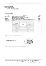
6.5 Display Quality 
  6.5.1 Test Conditions


1) Inspection Area: Within viewing area 

2) Condition 

: Same as test conditions shown in 4.1 and 6.2 

3) Test Pattern  : White display pattern (gray scale level L63) and black display pattern (gray scale level L0) 


  6.5.2 Specifications


4)


Item 

Description / Specifications 

Class 

Function No 

display, 

Malfunction 

Major 

Missing line 

Major 

Missing Sub-Pixels 

  1) Bright defects                                                  :    4pcs. Maximum 

2) Dark defects                                                    :    4pcs. maximum 

  3) Total sub-pixel defects                                    :    5pcs. Maximum 

 4) Bright defect conjunction(2sub-pixels)    :  1set max. 

 5) Dark defect conjunction(2sub-pixels)     :  1set max. 

 6) Bright defect conjunction(3sub-pixels)    :  0set 

 7) Dark defect conjunction(3sub-pixels)     :  0set 

8) Distance : Bright defect - Bright defect       


15 mm 

                          Dark defect - Dark defect           


10 mm 

                          Bright - Dark defect                      neglect 

Minor 

Display Quality

1)2)3)


Inconspicuous flicker, crosstalk, Newton's ring and other defects : 
neglect 

--- 

Black and White 

     Spots/line 

Inconspicuous defects : neglect 

--- 

Backlight Missing 

(Non-operating) 

Major 


    Note 1) Defects of both color filter and black matrix are counted as bright or dark defects. 

          Inspection area should be within the active area. 

    Note 2) Bright defect means a bright spot(sub-pixel) on the display pattern of gray scale L0. 

          Dark defect means a dark spot(sub-pixel) on the display pattern of gray scale L63. 

    Note 3) Bright spot which can not be found by using 5%ND-Filter shall not be counted as a defect. 

    Note 4) After the power of LCD is turned off, the last displayed image remains in the display for a few minutes. 

                  But this remained image is not Error. So phenomenon of remained display is not subject to display quality 

criteria. 


Summary of Contents for LTA057A341F

Page 1: ... Advantech Co Ltd CUSTOMER APPROVAL Specification for LTA057A341F Date of issue Nov 7 2008 Great Tech Corp 6F NO 309 Chuang Ching Rd Taipei Taiwan Tel 886 2 27299268 Fax 886 2 27298689 Customer Signature ...

Page 2: ...ification No TENTATIVE Sheet 1 Toshiba Matsushita Display Technology Co Ltd Date 2008 11 07 Date New No LTA057A341F 14 Old No Special Addition Change Revision History Date Rev Sheet New Item Old New Reason ...

Page 3: ...ized for applying to equipments for example nuclear control systems airplanes and space vehicles combustion control systems various safeguards medical equipment etc of which failures or malfunctions may directly threaten a human life or hurt a human body When using them for the above equipments consult with our company beforehand Understand that our company cannot take responsibility for the damag...

Page 4: ...ace may cause injuries 4 ABSOLUTE MAXIMUM RATINGS DO NOT EXCEED the absolute maximum ratings specified in this Specification These are the rated values that must not exceed for a LCD module by any means Since the parts used as a circuit are damaged by fire or breakage and the characteristic may not be recovered when exceeding this rating take into consideration the variation in ambient temperature...

Page 5: ...LEDs are lit and immediately after turned off the face of LCD module display surface top and bottom faces metal portions of right and left side faces and metal portion of LED unit cover s on the back are hot and require caution In case of touching working on such portion by necessity surely disconnect the power to the LCD module beforehand protect hands skin with low thermal conductive gloves etc ...

Page 6: ...e the fuse of suitable specification so that a fuse does not blow by the rush current at operation start Power Supply Recommended maximum output current of power supply Recommended Fuse Rating in case of using fuse for current limiter Built in Fuse Rating for reference VDD 4 0 A 1 5 A 1 5 A 2 SEQUENCE OF POWER SUPPLIES AND INPUT SIGNALS Power supply lines should be designed as follows Power suppli...

Page 7: ... cut onto the LCD module for outdoor operation Strong ultra violet radiation may damage the panel However in that case transmittance luminance will decrease Careful selection of material is required Don t expose any parts except the viewing area into the direct sunlight otherwise deterioration may occur 2 4 DESIGNING LED POWER SUPPLY CIRCUIT Make a design of stopping output when an LED driving cir...

Page 8: ...n film on an LCD panel near the last process of an assembly to prevent dust and scratch on the panel However remove the film in advance in case of a set attached a module is inserted into high temperature chamber for aging etc If it is left without removing the film it may cause irregular polarizer surface When removing the protection film peel off the film from its edge using round ended tweezers...

Page 9: ...play discolors or it causes spots Moreover moisture s infiltration into the inside causes failures 6 HANDLING IN THE CORROSIVE ATMOSPHERE Do not blow gas or do not use a LCD module beside the normal atmosphere It may cause failures 3 4 BENDING TWISTING OF LCD MODULE UNDER ASSEMBLY 1 INSTALLING LCD MODULE TO THE ENCLOSURE Do not bend or twist LCD module even momentary when LCD module is installed i...

Page 10: ...bles to connectors of a module A strong external force may damage internal connections of PCB or TAB driver Insert them correctly so that connectors for LCD module input signals and connection connectors of a set are not inserted oblique or half and be sure to check them When inputting signals etc without inserting them correctly it may cause failures of circuit parts 6 HANDLING FPC Be careful not...

Page 11: ...deteriorate display quality When it is necessary to store unavoidably for a long term in the state of packing by our company before opening store it within the range of 0 ºC to 35 ºC and in the dry place of 70 or less of relative humidity 2 SOLIDIFICATION ON THE LIQUID CRYSTAL IN CRYOGENIC CONDITION Since a temperature lower than a rated storage temperature described in this Specification may dama...

Page 12: ...ing 20 2 4 6 Interface Connector 21 2 4 7 Colors Combination Table 22 3 Recommended Operating Conditions 23 4 Electrical Characteristics 24 4 1 Test Conditions 4 2 Specifications 5 Optical Characteristics 25 5 1 Test Conditions 5 2 Optical Specifications 6 Quality 26 6 1 Inspection AQL 6 2 Test Conditions 6 3 Dimensional Outline 6 4 Appearance Test 27 6 4 1 Test Conditions 6 4 2 Specifications 6 5...

Page 13: ...clock DE Data Enable signal H sync V sync Synchronization signal R5 R4 R3 R2 R1 R0 Red display data G5 G4 G3 G2 G1 G0 Green display data B5 B4 B3 B2 B1 B0 Blue display data R L U D Reverse Scan Control Dimensional Outline 2 144 0 W 104 6 H 8 3 Max D mm Active Area 115 2 W 86 4 H mm Viewing Area 115 4 W 86 6 H mm Number of Pixels 3 320 W 240 H mm Pixel Pitch 3 0 36 W 0 36 H mm Pixel Arrangement 3 R...

Page 14: ...rage Temperature 2 TSTG 30 80 C Storage Humidity 2 HSTG 10 90 RH Note 1 Do not exceed the maximum rating values under the worst probable conditions taking into account the supply voltage variation input voltage variation variation in part constants and ambient temperature and so on Otherwise the module may be damaged Note 2 Wet bulb temperature should be 39 C Max and no condensation of water See f...

Page 15: ...ication No TENTATIVE Sheet 14 Toshiba Matsushita Display Technology Co Ltd Date 2008 11 07 Date New No LTA057A341F 14 Old No Special Addition Change 2 3 Mechanical Specifications 2 3 1 Weight 125 30g I LED mA ...

Page 16: ...ional Outline Unit mm front figure Standard Tolerance 0 5 Main viewing angle direction 12 5 8 144 104 6 1 5 6 2 1 2 1 2 1 5 2 5 4 4 60 6 22 89 4 7 6 4 5 7 8 3 MAX 4 diameter 5 90 2 Bezel Opening 86 4 Active Area 4 5 9 0 8 115 2 Active Area 119 Bezel Opening 14 4 0 8 14 4 12 5 4 R0 3 4 R0 3 depth max 3 1 4 diameter 1 6 2 8 3 MAX 8 3 MAX 10 4 12 3 4 hole depth max 3 1 ...

Page 17: ...a Matsushita Display Technology Co Ltd Date 2008 11 07 Date New No LTA057A341F 14 Old No Special Addition Change back figure Unit mm Standard Tolerance 0 5 1 6 CN1 CN2 1 136 6 3 7 8 3 96 4 4 1 12 7 1 4 5 1 49 1 1 33 depth max 4 2 4 diameter 2 6 ...

Page 18: ...ax 0ms min 40ms max DATA DE H V sync CLK U D L R V DD 0ms min 250ms min LED B L OFF ON 2 4 Electrical Specifications 2 4 1 Circuit Diagram 2 4 2 Sequence of Power Supplies and Signals Notes 1 When turn VDD on and turn it off the form of voltage should be input with no ripple signal I F Connector CN1 DC DC Manipulation Gray Scale Voltage Generation Circuit Converter Panel Controller LCD Panel CN2 L...

Page 19: ...atsushita Display Technology Co Ltd Date 2008 11 07 Date New No LTA057A341F 14 Old No Special Addition Change 2 4 3 Timing Chart tv tvw Vsync tvfp th tvd tvds tvblnk Hsync DE 1 2 239 240 th thw thde thds thfp 320 1 2 3 4 Hsync DE RGB Data NCLK tvd ...

Page 20: ...ds 5 0 ns Data Hold Time tdh 2 0 ns Note 1 If DE is fixed to H or L level for certain period while CLK is supplied the panel displays black with some flicker Note 2 Don t fix CLK to H or L level while the VDD 3 3V is supplied If CLK is fixed to H or L level for certain period while DE is supplied the panel may be damaged When It holds on DC voltage supplies to liquid crystal materials and It may c...

Page 21: ...als Terminal No Symbol Setting 30 R L L GND or NC Open 31 U D H 3 3V Up Down Reverse CN1 Reverse Scan Control Terminals Terminal No Symbol Setting 30 R L H 3 3V 31 U D H 3 3V Right Left Reverse CN1 Reverse Scan Control Terminals Terminal No Symbol Setting 30 R L L GND or NC Open 31 U D L GND or NC Open Up Down and Right Left Reverse CN1 Reverse Scan Control Terminals Terminal No Symbol Setting 30 ...

Page 22: ...9 GND 1 20 B0 2 BLUE DISPLAY DATA LSB 21 B1 2 BLUE DISPLAY DATA 22 B2 2 BLUE DISPLAY DATA 23 B3 2 BLUE DISPLAY DATA 24 B4 2 BLUE DISPLAY DATA 25 B5 2 BLUE DISPLAY DATA MSB 26 GND 1 27 DE DATA ENABLE 28 VDD 3 3V POWER SUPPLY 29 VDD 3 3V POWER SUPPLY 30 R L HORIZONTAL REVERSE L level or Open normal H level reverse 31 U D VERTICAL REVERSE L level or Open reverse H level normal 32 GND 1 33 NC 3 CN2 LE...

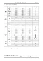
Page 23: ...L L L L L L L L L62 Gray Scale of Red Red H H H H H H L L L L L L L L L L L L Red L63 Black L L L L L L L L L L L L L L L L L L L 0 L L L L L L L L L L L H L L L L L L L 1 L L L L L L L L L L H L L L L L L L L 2 L3 L60 L L L L L L H H H H L H L L L L L L L61 Dark Light L L L L L L H H H H H L L L L L L L L62 Gray Scale of Green Green L L L L L L H H H H H H L L L L L L Green L63 Black L L L L L L ...

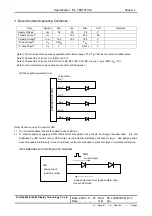
Page 24: ...o R0 G5 to G0 B5 to B0 CLK DE H sync V sync GND VSS 0V Note 4 One row LEDs six piece series connection at 25 degrees C LED back light equivalent circuit Note Cautions on use the circuit of LED 1 The current feedback function is needed to each LED line 2 To control brightness applying PWM Pulse Width Modulation drive should be strongly recommended If to dim brightness by LED current control LED whi...

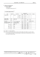
Page 25: ... Temperature Ta 25 5 C Ambient Humidity Ha 65 20 RH Supply Voltage VDD 3 3V Input Signal Refer typical value in 2 4 4 Timing Specifications LED Current ILED 15 0mA 4 2 Specifications Item Symbol Min Typ 1 Max Unit Remark Current Consumption IDD 150 220 mA VDD Terminal Current Note 1 The IDD is measured in the following pattern 1 White 2 Yellow 3 Purple 4 Red 5 Light Blue 6 Green 7 Blue 8 Black 1 3...

Page 26: ... Response Time tOFF θ 0 φ 0 25 35 ms Luminance L 320 400 cd m 2 IF 15mA Luminance Uniformity LUNF θ 0 φ 0 Gray Scale Level L63 White 60 70 xR 0 52 0 59 0 66 Red yR Gray Scale Level L63 θ 0 φ 0 0 27 0 34 0 41 xG 0 29 0 36 0 43 Green yG Ditto 0 48 0 55 0 62 xB 0 08 0 15 0 22 Blue yB Ditto 0 05 0 12 0 19 xW 0 25 0 32 0 39 Chromaticity White yW Ditto 0 27 0 34 0 41 Note 1 Refer to 11 Measuring Method ...

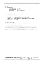
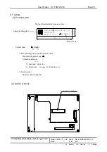
Page 27: ...perature 25 5 C 2 Ambient Humidity 65 20 RH 3 Illumination Approximately 500 lx under the fluorescent lamp 4 Viewing Distance Approximately 30cm by the eyes of the inspector from the module 5 Inspection Angle θ 0 φ 0 6 3 Dimensional Outline The products shall conform to the dimensions specified in 2 3 2 Definition of Major and Minor defects are as follows Item Description Class Important Dimension...

Page 28: ...der joint lead move when pulled Minor Bezel Frame Connectors Distinct stain rust or scratch which relate with LCD display performance and reliability Major Line width Length mm Acceptable count W 0 05 neglect 0 05 W 0 07 n 8 0 07 W 0 10 n 2 0 10 W L 3 2 Average diameter mm Acceptable count side D 0 2 neglect 0 2 D 0 35 n 5 0 35 D 0 5 n 2 0 5 D 0 Black and White Spots Lines 1 2 3 Minor Note 1 Inspe...

Page 29: ... 7 Dark defect conjunction 3sub pixels 0set 8 Distance Bright defect Bright defect 15 mm Dark defect Dark defect 10 mm Bright Dark defect neglect Minor Display Quality 1 2 3 Inconspicuous flicker crosstalk Newton s ring and other defects neglect Black and White Spots line Inconspicuous defects neglect Backlight Missing Non operating Major Note 1 Defects of both color filter and black matrix are co...

Page 30: ...re Operation 1 70 C 192 h OK 3p 3p High Temperature Storage 2 80 C 192 h OK 3p 3p High Temperature High Humidity operation 1 60 C 90 192 h OK 3p 3p Low Temperature Operation 1 20 C 192 h OK 3p 3p Low Temperature Storage 2 30 C 192 h OK 3p 3p Temperature Shock 2 30 C 80 C 50 cycles 0 5h 0 5h OK 3p 3p Mechanical Vibration 2 10 200 10Hz sweep cycle 1 5 9 8m s 2 constant X Y Z each directions 0 5h eac...

Page 31: ... 8 000001 c d c Manufacturing place code Production date Manufacturing place code Production date 8 H e f e Year code 2008 Æ 8 f Month code January Æ A December Æ L d Serial number Decimal system six figures 2 Label Locations Toshiba Matsushita Display Technology Co Ltd 35 7 5 MADE IN LTA057A341F 8H 000001 The liquid crystal display module number 2 dimensional symbol Product code Product Label ...

Page 32: ...s Ambient temperature 25 5 C No wind LED current 15mA Lighting condition continuous lighting 7 2 2 Specifications MTBF 20 000 h ILED 15mA Definitions of failure for judgment shall be as follows 1 LCD luminance becomes half of the minimum value specified in 5 2 2 LED doesn t light normally Note1 In case of LCD long period operation discoloration of light guide or optical sheet As the result there i...

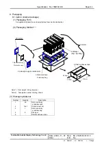
Page 33: ...tricity Protective sack 8 Packaging 8 1 Carton internal package 1 Packaging Form Corrugated cardboard box and polyethylene foam as shock absorber 2 Packaging Method 1 2 Note 1 Total weight 8 4kg Approx Note 2 Acceptable number of piling 10sets 3 Packaging Material Number Quantity Description 1 2 3 4 5 60 1set 1 8 Static electricity protective sack Holder inner box Static electricity protective bag...

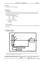
Page 34: ...uarantee our LCD module conform the regulation by itself a Examples of EMI Regulations FCC PART15 CLASS B VCCI CLASS B CISPR CLASS B b Examples of Safety Regulations IEC 60950 UL 60950 10 2 Environment This LCD module is not used or contained over maximum concentration value of any substance prohibited by RoHS s Requirement 11 Measuring Method 11 1 Measuring System 1 The measurement point is the c...

Page 35: ...t shall be executed 30 minutes after the LED is lit up 2 Contrast Ratio The contrast ratio can be calculated by the following expression Contrast Ratio CR L63 L0 L63 Luminance on the white raster gray scale level L63 L 0 Luminance on the black raster gray scale level L0 3 Viewing Angle Viewing angle is defined as the angles θ φ in which specified contrast ratio can be obtained Refer to 11 1 3 for ...

Page 36: ...tector photodiode which measures the light intensity of the pixels tON Turn on time is the time for the light intensity of the pixels to go from 90 of its maximum to 10 of its maximum tOFF Turn off time is the time for the light intensity of the pixels to go from 10 of its maximum to 90 of its maximum Photodiode S1223 01 HAMAMATSU PHOTONICS K K White Display White Raster gray scale level L63 Black...

Page 37: ......

Page 38: ......

Reviews: