2-2
1-1-2. Preparation before Adjustment
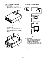
<Opening the CCU>
1. Remove all cables connected to CCU.
2. Remove one scrwe (2) fixing the unit cover
(1).
Fig. 5
3. Turn over the unit.
4. Remove four screws (3) fixing the unit cover
(1).
5. Pull the mechanical chassis (4) in the arrow
direction.
Fig. 6
1-1-3. Equipment Connection Diagram
Fig. 7
1-1-4. Initial Setting
1. Perform the warming up for approx. 5 min-
utes with the POWER switch turned “ON”
before performing the adjustments.
2. When the chart is illuminated unevenly, the
correct adjustment cannot be performed. So
set the light equipments to give an even
illumination.
Note:
Perform the adjustments in a location with less
dust to prevent inside of the camera head from
dirty.
Lens
Camera
head
Camera control unit
VIDEO
DC IN12V
DC power supply
Waveform monitor (WFM)
Vector scope
Color monitor
75W termination
(2)
(1)
(3)
(3)
(4)
(1)
Summary of Contents for IK-TU51CU
Page 4: ...1 1 SECTION 1 GENERAL DESCRIPTION IK TU51CU ...
Page 5: ...1 2 ...
Page 6: ...1 3 ...
Page 7: ...1 4 ...
Page 8: ...1 5 ...
Page 9: ...1 6 ...
Page 10: ...1 7 ...
Page 11: ...1 8 ...
Page 12: ...1 9 ...
Page 13: ...1 10 ...
Page 14: ...1 11 ...
Page 15: ...1 12 ...
Page 16: ...1 13 ...
Page 17: ...1 14 ...
Page 18: ...1 15 ...
Page 19: ...1 16 ...
Page 20: ...1 17 ...
Page 21: ...1 18 ...
Page 22: ...1 19 ...
Page 23: ...1 20 ...
Page 24: ...1 21 ...
Page 25: ...1 22 ...
Page 26: ...1 23 ...
Page 27: ...1 24 ...
Page 28: ...1 25 JK TU52H ...
Page 29: ...1 26 ...
Page 30: ...1 27 JK TU53H ...
Page 31: ...1 28 ...
Page 41: ...3 2 1 2 Packing Assembly JK TU52H JK TU53H Y110 A701 A702 ...
Page 43: ...3 4 1 4 Camera Head Assembly JK TU52H A110A A110A A116A A111A A111 A116 A110 A113 PF01 PF01 ...
Page 44: ...3 5 1 5 Camera Head Assembly JK TU53H A113 A110 A110A PF01 PF01A PF01 A111 A111A A111A ...
Page 54: ...4 2 1 3 Rear PC Board IK 528A Component Side Soldering Side ...
Page 55: ...4 3 1 4 Driver PC Board Component Side ...
Page 56: ...4 4 Soldering Side ...
Page 57: ...4 5 1 5 DSP PC Board Component Side ...
Page 58: ...4 6 Soldering Side ...
Page 59: ...4 7 2 BLOCK DIAGRAMS 2 1 Power Supply Block Diagram ...
Page 60: ...2 2 TG SG Block Diagram 4 8 4 9 ...
Page 61: ...2 3 Pre Process Block Diagram 4 10 4 11 ...
Page 62: ...2 4 ENC Output Block Diagram 4 12 4 13 ...
Page 63: ...2 5 DSP Block Diagram 4 14 4 15 ...
Page 64: ...2 6 Memory Block Diagram 4 16 4 17 ...
Page 65: ...4 1 2 7 Auto Block Diagram 4 18 ...
Page 66: ...4 2 2 8 D Out Block Diagram 4 19 ...
Page 67: ...4 20 4 21 3 CIRCUIT DIAGRAMS 3 1 Overall Wiring Diagram ...
Page 68: ...4 22 4 23 3 2 Power Supply Circuit Diagram ...
Page 69: ...3 3 TG Circuit Diagram 4 24 4 25 4 26 ...
Page 70: ...4 27 4 28 4 29 3 4 SG Circuit Diagram ...
Page 71: ...4 30 4 31 3 5 Pre Process Circuit Diagram ...
Page 72: ...4 32 4 33 4 34 3 6 ENC Circuit Diagram ...
Page 73: ...4 35 4 36 3 7 Output Circuit Diagram ...
Page 74: ...4 37 4 38 4 39 3 8 DSP Circuit Diagram ...
Page 75: ...4 40 4 41 4 42 3 9 Memory Circuit Diagram ...
Page 76: ...4 43 4 44 3 10 Auto Circuit Diagram ...
Page 77: ...4 45 4 46 3 11 D Out Circuit Diagram ...
Page 78: ...4 1 3 12 Rear Circuit Diagram 4 47 ...
Page 79: ...SECTION 5 SPECIFICATIONS 1 SPECIFICAIONS IK TU51CU JK TU52H JK TU53H ...
Page 80: ......

