background image

- 3

1

 -

- 3

2

 -

21

20

20

21

1

GND

SY_E5

GND

SC_E5

SW_E5

GND

V_E5

GND

1

A

14

15

1

48

39

38

25

24

12

NC

+

L_E5

R_E5

TUNER GND

TUNER GND

12

GND

GND

NC

9V-1

32V

ACDETECT

5V-3

5V-3

GND

6

7

17

V

+

2

1

1

2

L

R

+

23590293

PD2206   -1

+

TP-12

16

9

8

1

6

1

GND

NC

SOUND GND

SOUND GND

26V

26V

50

1

NC

L_AUDIO

R_AUDIO

   GND

+

GND

+

1

5

1

10

40

+

50

10

20

30

20

40

11

12

+

+

30

+

1

2

+

+

5V-1

GND

1

2

3

+

+

1

6

11

15

10

5

1

1

1

5V2

9V
-1

1

3

GND

RV255

RV251

CV51

QV23

GR

V49

GRV47

GRV46

CV52

RV254

CV58

RV257

R

V253

CV91

LV
1

5

QV24

QV22

QV21

RV256

RV258

RV252

LV23

GR

V55

GR

V56

LC04

GRV74

LV21

R

V76

CV25

GR

V33

GR

V57

QV55

LV03

RV
8

3

CV26

GR

V01

CV23

RV84

LV24

RV78

RV
7

1

RV
8

1

CV03

GR

V54

GR

V04

RV
8

0

GR

V06

CV54

LV01

CV55

RV
8

2

GR

V31

QV54

R

V72

R

V77

CV21

LC05

GR

V48

R

V85

GR

V32

GR

V05

CV02

LV17

LV
0

2

GR

V02

CV59

QV16

GR

V36

QV15

GR

V73

CV27

CV20

CV22

RV
7

9

CV56

CV57

CV24

GR

V03

GRV78

GRV79

R512

LV33

C529

R514

Q504

CC20

R511

C504

C506

C503

C521

C501

C530

R502

Q501

C519

C527

CC31

C526

C517

R508

C505

R506

R507

GR103

L105

RV
2

5

9

L104

C107

LV16

GR

V44

RV
2

6

0

Q4103

GR102

GRV75

C104

Q4101

GR

V50

LV
2

2

GR

V45

GR03

GR02

L106

LV28

LV
2

5

GR

V30

GR

V59

CV60

LV
1

0

GR

V60

GR

V76

LV32

GR

V69

GR

V61

GR

V51

RB576

GR

V58

RB575

LV
3

1

GR

V65

GR

V63

GR113

LV
2

6

GR

V66

CV17

QV14

LV29

GR

V71

CV13

LV
1

2

CV28

GR

V70

GR

V62

QB517

GR

V77

GR

V68

CV19

LV
2

7

GR

V67

GR

V64

GR

V43

LV
3

0

CB512

C663

LC06

C631

RR05

GJ413

RR04

C4111

R4122

GJ414

R4104

Q4109

R4120

R4109

R4103

Q4108

R4123

C4112

R4108

R4121

RR06

GR

V40

GR

V42

LV
2

0

DR43

GR112

LV18

LV
1

9

GR

V39

GR

V37

GR

V41

DR42

GR

V38

DR41

PJ22A

PJ60A

RV255

RV251

CV51

PH02

GR

V49

GRV47

GRV46

CV52

RV254

CV58

LV16

RV257

R

V253

CV91

PH01

LV15

QV24

QV22

QV21

P517

RV256

RV252

LC04

GRV74

LV21

R

V76

CV25

GR

V33

GR

V57

QV55

LV03

R

V83

CV26

GR

V01

CV23

RV84

LV24

R

V71

R

V81

CV03

GR

V54

GR

V04

PV25A

RV80

GR

V06

CV54

LV01

CV55

R

V82

GR

V31

QV54

RV
7

2

R

V77

CV21

LC05

GR

V48

R

V85

GR

V32

GRV05

CV02

LV17

LV02

GR

V02

CV59

QV16

GR

V36

QV15

GR

V73

CV27

CV20

CV22

R

V79

CV56

CV24

GR

V03

GRV78

GRV79

R512

LV33

C529

R514

Q504

CC20

R511

P803B

C504

X501

C506

L505

P515B

RV78

C503

C521

C501

C530

C514

R502

Q501

C519

C527

CC31

C526

C517

R508

C505

R506

R507

CV57

GR103

C6605

C105

QV23

L105

R

V259

L110

L104

C107

GR

V44

PV02

R

V260

Q4103

C668

GR102

GRV75

C104

Q4101

GR

V50

LV22

R

V258

GR

V45

GR03

GR02

L106

LV28

LV25

LV23

GR

V55

GR

V56

GR

V30

GR

V59

CV60

LV10

LT01

DR43

GR

V60

PK02

GR

V76

LV32

GR

V69

GR

V61

GR

V51

RB576

GR

V58

RB575

LV31

GR

V65

GR

V63

C119

GR113

LV26

GR

V66

CV17

QV14

LV29

GR

V71

CV13

LV12

CV28

GR

V70

GR

V62

QB517

GR

V77

GR

V68

CV19

LV27

GR

V67

GR

V64

GR

V43

LV30

CB512

PJ22A

P804B

C680

C682

C663

C612

C671

PJ60A

Q610A

C666

Q610

LC06

C665

C674

C631

C688

C681

P601A

C687

RR05

C102

GJ413

RR04

C4111

R4122

PK01

GJ414

R4104

Q4109

R4120

R4109

P662

R4103

Q4108

R4123

L101

C4112

PV90

R4108

R4121

RR06

GR

V40

GR

V42

LV20

GR112

LV18

LV19

GR

V39

P516B

GR

V37

GR

V41

DE99

DR42

GR

V38

PJ21A

DR41

H001

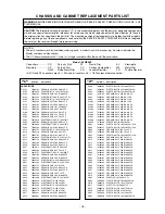
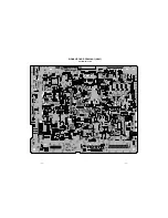
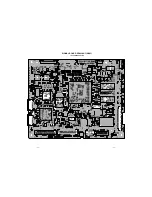
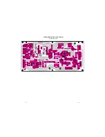
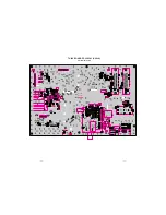
TN/AV BOARD PD2206A1 (U003A)

TOP (COMPONENT) SIDE

Summary of Contents for 42WP56P

Page 1: ...SERVICE MANUAL Plasma Color Television 42WP56P FILE NO 030 200507 Published in Japan Sep 2005 YC TOSHIBA CORPORATION 2005 ...

Page 2: ... 5 LOCATION OF CONTROLS 10 LAYOUT OF MAJOR BOARDS 12 MECHANICAL DISASSEMBLY 13 EXPLODED VIEW 15 PACKING DISASSEMBLY 17 CHASSIS AND CABINET REPLACEMENT PARTS LIST 18 PC BOARDS TOP BOTTOM VIEW 23 CIRCUIT BLOCK DIAGRAM 37 SPECIFICATIONS 38 APPENDIX SCHEMATIC DIAGRAM ...

Page 3: ...f injury or where there could be physical damage in the event of operational error Physical damage means major damage to a home furnishings and other possessions Examples of marks SHOCK HAZARD PROHIBIT DISASSEM BLING UNPULUG The indicates caution including danger and warning The actual meaning of this caution is indicated inside the or nearby illustrations or text The example shown to the left ind...

Page 4: ...ark is included in a circuit diagram or parts list Parts mounting and routing of the wiring should be the same as that used originally For safety purposes insulating materials such as tubing or tape is sometimes used and printed circuit boards are sometimes mounted floating Also make sure that wiring is routed and clamped to avoid parts that generate heat and which use high voltage Always follow t...

Page 5: ...isplayed differently as shown below de pending on the setting of the receiving color system COLP PAL COLC NTSC COLS SECAM Automatic A D Adjustment PC Component 7 button Self diagnostic display ON OFF 9 button CAUTION Never try to perform initialization unless you have changed the memory IC SERVICE MODE 1 ENTERING SERVICE MODE 1 Press button once on 2 Press button again and 3 While pressing the but...

Page 6: ...WER button to turn off the TV once INITIALIZATION OF MEMORY DATA After replacing EEPROM IC the following initialization is required 1 Enter the service mode then select any register item 2 Press and hold the CALL button on the Remote then press the CHANNEL s button on the TV The initialization of EEPROM IC has been complated 3 Check the picture carefully If necessary adjust any adjustment item abo...

Page 7: ... Operation number of protecting circuit 000 is normal When indication is other than 000 overcurrent apt to flow and circuit parts may possibly be damaged 4 Bus line OK is normal SCL GND Red indication SCL GND short circuit SDA GND Red indication SDA GND short circuit SCL SDA Red indication SCL SDA short circuit 5 Bus cont OK is normal NG is abnormal Red indication when type name of semiconductor i...

Page 8: ...EPROM Version information of EEPROM Display 1 byte data 3 SUB MPU Version information of SUB MPU Display 1 byte data 4 OPTION Option information Display six numbers of 1 byte data 5 HDMI ID HDMI ID information Display 4 byte data 6 CD number Display 8 digit number 7 Model name Display 7 digit number 8 Panel Vender information display The following Panel Vender and screen size are displayed WP56_EU...

Page 9: ... information Display RF position number 0 99 on the main screen or Input Source EXT1 2 3 HDMI etc 2 MAIN FORMAT Display Video and PC format information 3 MAIN PLL Main PLL information Display five numbers of 1 byte data 4 SCREEN SIZE Display the screen size as follows 5 OTHER STATUS Other status information Display three numbers of 2 byte data Super live Cinema Subtitle 14 9 Wide 4 3 EXT1 1080i 50...

Page 10: ...e f Standby RED Power On GREEN On timer set INPUT 3 EXT 3 media recorder decoder SCART 1 EXT 1 SCART 2 EXT 2 BRACKET HOLES SAT IN OUT MEDIA REC TV MAINS LEAD SUPPLIED CONNECTING EXTERNAL EQUIPMENT CONTROLS AND INPUT CONNECTIONS ...

Page 11: ...ramme For On Standby mode To display text services When using a TOSHIBA VCR or DVD press mto PAUSE press wto EJECT press lqto SKIP REWIND presssl to SKIP FORWARD pressrto PLAY presspto STOP press qto REWIND presssto FAST FORWARD To change programme positions and text pages To alter the volume When using menus the arrows move the cursor on the screen up down left or right OK to confirm your selecti...

Page 12: ... 12 LAYOUT OF MAJOR BOARDS U003D RMT LED BOARD U003A TN AV BOARD U001 SIGNAL BOARD U003B FRONT AV BOARD U002 LOWB BOARD U003C KEY BOARD ...

Page 13: ...3 A206 A206 MECHANICAL DISASSEMBLY 1 Remove the stand foot and back cover 2 Remove the boards LOWB TN AV FRONT AV KEY and piece key ass y BITTB3 12 ECO 2 BITTB3 8 ECO 2 PP4 8 ECO PP3 8 SBN PP3 8 ECO 8 PP4 8 SBN 2 PP4 12 SBN 2 BITTB3 12 SBN 4 PP3 8 ECO 2 PP3 8 ECO 6 H001 U800 U003C U003A U003B A221 A220 ...

Page 14: ...PP3 8 ECO 4 PP3 8 ECO 6 U001 U002 W662 W661 BITTB3 8 SBN 6 BITTB3 12 ECO 2 BITTB3 8 SBN 6 U003D 3 Remove the boards SIGNAL RMT LED and speaker 4 Remove the display BITTB4 12 ECO 4 BITTB4 12 ECO 19 B001 A201 ...

Page 15: ...5 EXPLODED VIEWS 1 Chassis Block PP4 8 SBN 6 PP6 35 SW W SBN 4 BITTB4 12 SBN 14 PP3 8 SBN PP4 8 SBN 9 BITTB4 12 SBN 7 A401 W662 A403 A410 W661 BITTB3 8 SBN 6 BITTB3 12 ECO 2 BITTB3 8 SBN 6 U003D A206 A206 ...

Page 16: ... 4 BITTB3 8 ECO 2 PP4 8 ECO PP3 8 SBN PP3 8 ECO 8 PP4 8 SBN 2 PP4 12 SBN 2 PP3 8 ECO 6 BITTB3 12 SBN 4 PP3 8 ECO 2 BITTB4 12 ECO 4 BITTB4 12 ECO 19 PP3 8 ECO 6 H001 B001 U800 U001 A221 U003C U003A U003B A201 U002 A220 2 Main Block ...

Page 17: ... 17 PACKING DISASSEMBLY A701B A701A A702B A702B A702A A702A A705 A705 Y110 Y101 Y130 Y170 Y174 ...

Page 18: ...9102 CERAMIC CHIP 50V B 1000PF K C606 76109102 CERAMIC CHIP 50V B 1000PF K C612 76664102 ELECTROLYTIC 6 3V 1000UF M 3A C631 76619102 ELECTROLYTIC CHIP 16V 47UF M C632 76092731 CERAMIC CHIP 16V B 1UF K C651 76092463 CERAMIC CHIP 16V B 0 22UF K C652 76092463 CERAMIC CHIP 16V B 0 22UF K C653 76092538 CERAMIC CHIP 10V F 1UF Z C662 76109102 CERAMIC CHIP 50V B 1000PF K C663 76619100 ELECTROLYTIC CHIP 16...

Page 19: ...0 76011102 CHIP 1 20W 1K OHM J R651 76011473 CHIP 1 20W 47K OHM J R652 76011103 CHIP 1 20W 10K OHM J R653 76011223 CHIP 1 20W 22K OHM J R654 76011103 CHIP 1 20W 10K OHM J R655 76011222 CHIP 1 20W 2 2K OHM J R660 76011473 CHIP 1 20W 47K OHM J R662 76011103 CHIP 1 20W 10K OHM J R663 76011473 CHIP 1 20W 47K OHM J R664 76011104 CHIP 1 20W 100K OHM J R667 76011104 CHIP 1 20W 100K OHM J R670 76011472 CH...

Page 20: ...2 76871181 CHIP 1 8W 180 OHM J RV84 76011101 CHIP 1 20W 100 OHM J RV85 76011473 CHIP 1 20W 47K OHM J RV90 76366750 CARBON FILM 1 6W 75 OHM J RV90A 23965241 TAPE CC 12 10MM L30M RV91 76366750 CARBON FILM 1 6W 75 OHM J RV92 76011103 CHIP 1 20W 10K OHM J RV93 76011392 CHIP 1 20W 3 9K OHM J RV94 76011103 CHIP 1 20W 10K OHM J RV95 76011392 CHIP 1 20W 3 9K OHM J RV121 76872750 CHIP 1 16W 75 OHM J RV129 ...

Page 21: ...499 DIODE ERB12 01 DE07 23357683 DIODE ZENER RD3 3ESA B1 DE60 23357810 DIODE FMB G14L DE61 23357697 DIODE 1SS133 DE62 23357845 DIODE ZENER MTZJ7 5B DE85 23357861 DIODE ZENER MTZJ11A DE86 23357697 DIODE 1SS133 DE99 23357840 DIODE ZENER MTZJ6 2B DV01 23357703 DIODE 1SS355 DV02 23357703 DIODE 1SS355 DV03 23357703 DIODE 1SS355 DV04 23357703 DIODE 1SS355 DV120 23357745 DIODE ZENER MA8056 M MISCELLANEOU...

Page 22: ...3344507 SWITCH PUSH SKHHLMA010 SA06 23344507 SWITCH PUSH SKHHLMA010 SA07 23344507 SWITCH PUSH SKHHLMA010 U800 23122502 POWER UNIT POWER BLOCK MODULE 1H276W W661 23351320 SPEAKER ASSY 6X12 8 OHM 10W SPK 1468AO W662 23351320 SPEAKER ASSY 6X12 8 OHM 10W SPK 1468AO X501 23153612 CRYSTAL 16 200 25PPM 25OHM ZA01 23103778 FERRITECORE TFE1008 ZA02 23103839 FERRITECORE TFE1012 ZA07 23103840 FERRITECORE TFE...

Page 23: ...SIGNAL BOARD PD2238H1 U001 BOTTOM FOIL SIDE 23 24 ...

Page 24: ...SIGNAL BOARD PD2238H1 U001 TOP COMPONENT SIDE 25 26 ...

Page 25: ...B E E B 1 2 3 4 5 6 1 2 3 4 5 6 7 8 9 10 11 7 1 1 3 3VD b NC 20V 20V GND 32V GND 6VD GND 3 3VD a 1 2 3 4 5 ACDETECT DE10 RE07 CE87 RE06 DE20 P822 DE14 DE87 CE86 DE07 QE86 RE87 DE06 DE05 CE05 CE85 RE14 DE89 RE20 P821 P820 CE08 DE04 P819 RE05 RE09 RE86 P807A RE08 DE85 QE85 DE09 P818 DE08 RE30 CE70 CE71 LE71 RE70 RE61 DE74 CE32 CE72 DE88 PP81 FE20 LE70 LE30 CE60 LE31 RE74 DE31 CE63 QE70 DE61 QE60A DE...

Page 26: ...24 R4101 Q161 C164 RC02 R6616 C668 R4107 R6617 LC29 LC28 CC74 CC62 Q656 R661 R660 R6615 Q655 R103 GC01 Q6601 Q102 CC60 R167 LC23 CC65 CC64 RV32 RT02 R6631 R4106 C118 GR26 GR25 GR27 GR07 C1807 GRR44 GR06 C1808 C1806 GR28 C101 P516B D101 C110 R101 DE99 R102 C1802 PJ21A GR612 H001 C102 RC40 Q4102 CC40 PK01 GR611 GR610 R4105 RC41 CC41 RR02 P662 DR44 GRR05 RR03 L101 R4100 PV90 GRR04 DR45 RR01 Q4100 C52...

Page 27: ...4 C4111 R4122 GJ414 R4104 Q4109 R4120 R4109 R4103 Q4108 R4123 C4112 R4108 R4121 RR06 GRV40 GRV42 LV20 DR43 GR112 LV18 LV19 GRV39 GRV37 GRV41 DR42 GRV38 DR41 PJ22A PJ60A RV255 RV251 CV51 PH02 GRV49 GRV47 GRV46 CV52 RV254 CV58 LV16 RV257 RV253 CV91 PH01 LV15 QV24 QV22 QV21 P517 RV256 RV252 LC04 GRV74 LV21 RV76 CV25 GRV33 GRV57 QV55 LV03 RV83 CV26 GRV01 CV23 RV84 LV24 RV71 RV81 CV03 GRV54 GRV04 PV25A...

Page 28: ...3B TOP COMPONENT SIDE 23547853 VOL DOWN VOL UP CH DOWN R 1786 CH UP NC POWER_KEY ADC_IN1 GND ADC_IN2 KEY_FGND 4 5 6 POWER VIDEO MENU 3 2 1 RA72 RA73 SA04 SA02 SA03 RA74 SA01 RA71 RA77 SA07 PJ42B SA06 SA05 RA79 RA78 RA72 RA73 RA74 RA71 RA77 RA79 RA78 PD2206 3 1 VIDEO MENU POWER 23590293 6 KEY_FGND ADC_IN2 GND ADC_IN1 POWER_KEY NC CH UP CH DOWN VOL UP VOL DOWN SA07 SA06 SA05 PJ42B SA04 SA02 SA03 SA0...

Page 29: ... indicated to chassing ground using a color bar signal with all controls at normal line voltage 220 volts 5 Waveforms are taken receiving color bar signal with enough sensitivity 6 Voltage reading shown are nominal values and may vary 20 except H V MODEL 42WP56P SCHEMATIC DIAGRAM WARNING BEFORE SERVICING THIS CHASSIS READ THE SERVICE SAFETY PRECAUTIONS ON PAGE 3 OF THIS MANUAL CAUTION The internat...

Page 30: ...26 52 EEPROM1 SHEET 309 27 52 EEPROM2 SHEET 310 28 52 MICRO I O SHEET 400 29 52 OCM MEMORY I F SHEET 401 30 52 FLASH MEMORY SHEET 402 31 52 SYNC SEPA SHEET 403 32 52 E2P OTHER SHEET 404 33 52 STD BY MICOR SHEET 405 34 52 CORTEZ REG 1 SHEET 406 35 52 CORTEZ REG 2 SHEET 407 36 52 CORTEZ REG 3 SHEET 408 37 52 BOOT CONFIG SHEET 409 38 52 SERVICE CONNECTOR SHEET 410 39 52 I2C Switch SHEET 411 40 52 AUD...

Page 31: ...ess PDP PANEL PDP PANEL TIF AUDIO AMP LOWB BOARD LOWB BOARD POWER UNIT POWER UNIT 1H276W 1H276W TN AV BOARD TN AV BOARD AC INPUT AC INPUT QV01 Vidio SW CORTEZ BOARD CORTEZ BOARD Vs 190V Va 65V Vcc 5v 32V 26V 12V 5V 1 32V 26V 9V 1 9V 2 12V 5V 1 5V 1 RGB PC C1 C2 1 2 3 WOOFER MONITOR AUDIO MSP Q501 VCD QS01 Audio SW ADC CIRCUIT BLOCK DIAGRAM ...

Page 32: ...put Side 4 pin S video Phono jack Video Phono jacks Audio L R PC Input Mini D sub 15 pin Analog RGB signal Input 3 5mm stereo jack Audio Programme Positions 100 Stereo Nicam 2 carrier system Visible Screen Size 105cm approx Display 16 9 Sound output at 10 distortion Main 10W 10W Power consumption 315W as specified in EN60107 1 1997 Standby approx 1W Dimension 78cm H 110cm W 39cm D approx Height di...

Page 33: ......

Reviews: