

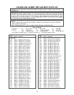


32V
GND
12
NC
R_E5
L_E5
TUNER GND
TUNER GND
12
+
ACDETECT
9V-1
NC
GND
5V-3
GND
5V-3
SW_E5
SC_E5
GND
SY_E5
GND
GND
V_E5
GND
1
20
19
21
20
19
21
6
GND
NC
SOUND GND
SOUND GND
26V
26V
1
GND
5V-1
+
+
+
L_AUDIO
GND
+
1
5
R_AUDIO
NC
GND
+
12
11
+
+
1
2
+
1
23547853
R-1786
14:SIF out
15:32V
16:IF out
17:VIDEO out
TP-12
+
17
7
6
3
2
3
1
+
2
1
+
+
2:NC
3:5V
4:NC
5:SW1
6:SW2
7:VT
8:RF AGC
9:NC
10:SCL
11:SDA
12:AFT
13Audio det out
5V2
GND
9V
-1
3
1
3
2
+
11
6
10
15
5
1
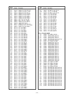
C524
P803B
X501
L504
C502
R518
L505
P515B
R504
R519
C514
R505
L502
R501
C1801
C516
PV25A
R
V70
R
V74
R
V07
CV63
RV94
QV52
RV95
RV93
PH02
D
V04
RV21
D
V02
R
V51
D
V01
LC01
R
V04
R
V58
RV53
RV31
R
V57
PH01
RV52
QV51
RV30
R
V05
RV55
LC02
R
V02
R
V59
GR
V72
RV73
RV54
R
V56
R
V03
RV28
RV92
P517
RC03
CV62
R
V13
D
V03
R
V06
R650
D613
D641
C602
C117
C1805
GR08
Q622
C678
R664
P804B
C652
C601
R681
R6606
Q665
D675
C680
R697
Q621
C682
R652
C651
R670
C653
C612
C671
R675
R671
R653
Q610A
C1803
R6605
R6603
D674
C662
R651
C666
Q610
R654
Q664
LC03
R667
C1804
R673
R685
Q612
Q672
D640
C690
R655
C696
Q671
C665
C674
R676
R684
GR05
D607
C688
C677
D615
R677
C681
P601A
D612
C632
C687
C694
QT02
L103
R
T05
LT01
QT05
RT12
CT02
QT01
QT04
R672
PK02
RB577
C113
R
T04
R105
RT09
R113
R108
C119
C111
R162
Q162
Q101
R170
CT01
CT09
CT06
C112
GT01
C162
CT08
R111
QT03
RT11
R115
GR613
C163
RT10
RT06
CT03
R680
R112
QT06
CT04
GT02
RB578
R104
CT07
RT07
CT05
RT08
R114
R6611
RS23
R166
LC27
R4102
R6634
R163
Q6602
LC30
RS25
R
T03
R107
C6605
D6601
C161
RC04
C105
LC21
RS26
Q654
Q6603
R6632
L110
R164
CC66
C115
R6614
D6602
R161
L190
GRR01
R6613
R165
LC22
CC61
R169
R663
C116
C103
C190
GC02
RS24
GR101
PV02
RC01
R6612
C114
GRR03
GRR02
CC75
L102
R
T01
R662
R6610
R6633
R168
CC67
CC63
LC24
R4101
Q161
C164
RC02
R6616
C668
R4107
R6617
LC29
LC28
CC74
CC62
Q656
R661
R660
R6615
Q655
R103
GC01
Q6601
Q102
CC60
R167
LC23
CC65
CC64
R
V32
RT02
R6631
R4106
C118
GR26
GR25
GR27
GR07
C1807
GRR44
GR06
C1808
C1806
GR28
C101
P516B
D101
C110
R101
DE99
R102
C1802
PJ21A
GR612
H001
C102
RC40
Q4102
CC40
PK01
GR611
GR610
R4105
RC41
CC41
RR02
P662
DR44
GRR05
RR03
L101
R4100
PV90
GRR04
DR45
RR01
Q4100
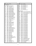
C524
L504
C502
R518
R504
R519
R505
L502
R501
C1801
C516
RV
7
0
RV
7
4
R
V07
CV63
RV94
QV52
RV95
RV93
D
V04
RV21
D
V02
RV51
DV
0
1
LC01
RV
0
4
R
V58
RV53
RV31
R
V57
RV52
QV51
RV30
R
V05
RV55
LC02
RV
0
2
R
V59
GR
V72
RV73
RV54
R
V56
RV
0
3
RV28
RV92
CV62
RV
1
3
D
V03
R650
D613
D641
C602
C117
GR08
Q622
C678
R664
R672
C652
C601
R681
R6606
Q665
D675
R697
Q621
R652
C651
R670
C653
R675
R671
R653
R6605
R6603
D674
C662
R651
GRR44
R654
Q664
LC03
R667
C1804
R673
R685
Q612
Q672
D640
C690
R655
C696
Q671
R676
R680
R684
D607
C677
D615
R677
D612
C632
C694
R166
QT02
L103
R163
RT
0
5
R
T03
R107
QT05
RT12
CT02
QT01
C161
QT04
RB577
C113
RT04
R105
R164
C115
R161
RT09
L190
R113
R108
R165
R169
C116
C111
C103
R162
C190
Q162
R101
Q101
R170
CT01
C114
CT09
L102
RT
0
1
R168
CT06
C112
GT01
Q161
C164
C162
CT08
R111
QT03
RT11
R115
GR613
C163
RT10
R103
RT06
CT03
R112
Q102
QT06
CT04
GT02
R167
RB578
R104
CT07
R
T07
CT05
RT02
RT08
R114
R6611
RS23
LC27
R6634
Q6602
LC30
RS25
D6601
RC04
LC21
RS26
Q654
Q6603
R6632
CC66
R6614
D6602
GRR01
R6613
LC22
CC61
R663
GC02
RS24
GR101
RC01
R6612
CC75
R662
R6610
R6633
CC67
CC63
LC24
RC02
R6616
R6617
LC29
LC28
CC74
CC62
Q656
R661
R660
R6615
Q655
GC01
Q6601
CC60
RC03
LC23
CC65
CC64
RV
3
2
R6631
RV
0
6
C118
GR26
C1805
GR25
GR27
GR07
C1807
C1803
GR06
C1808
C1806
GR05
GR28
C101
D101
C110
R102
C1802
GR612
R4102
RC40
Q4102
CC40
GR611
GR610
R4105
RC41
GRR03
GRR02
CC41
RR02
R4101
DR44
R4107
GRR05
RR03
R4100
GRR04
DR45
RR01
Q4100
R4106
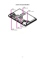
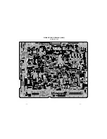
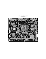
TN/AV BOARD PD2206A1 (U003A)
BOTTOM (FOIL) SIDE
-
29
-
- 3
0
-


