8
20AR20/30
SERVICE ADJUSTMENT
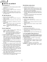
VCO Adjustment
1. Connect a digital voltmeter between pin (44) of IC201
and ground.
2. Receive a good local channel.
3. Enter the service mode and select the service
adjustment "S10".
4. Adjust the data so that digital voltmeter reads 2.2V.
5. Adjustment is completed, remove the voltmeter, return
to "normal" mode.
RF AGC Adjustment
1. Receive a good local channel.
2. Enter the service mode and select the service
adjustment "S08".
3. Set the data value to point where no noise or beat
appears.
4. Select another channel to confirm that no noise or
beat appears.
Note 1 :
You will have to come out of the service
mode to select another channel.
Note 2 :
Setting the data to "00" will produce a black
raster.
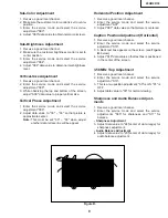
Screen Adjustment
1. Connect a digital voltmeter between TP852 and
TP853 on the CRT socket PWB.
Note :
These test points may not be provided.
Then connect the voltmeter to both ends of
R852 located near Q852 on the foil side.
2. Receive a good local channel.
3. Enter the service mode and select the service
adjustment "S03" and set the data value to "00" to
set the color level to minimum. (Record original data
code under adjustment "S03" before changing) You
may skip this step, if you selected a B/W picture or
monoscope pattern.
4. Select the service adjustment "S19" and adjust the
data value to "01", this turn off the luminance signal
(Y-mute).
5. Select the service adjustment "S04" and adjust data
value to obtain 0.17 volts on the oscilloscope screen.
6. Adjust the master screen control until the raster
darkens to the point where raster is barely seen.
7. Adjust the service adjustments "S11" red, "S12" green
and "S13" blue to obtain a good grey scale with
normal whites at low brightness level.
8. Select the service adjustment "S19" and reset data
to "00". Select the service adjustment "S03" and reset
data to obtain normal color level.
9. Remove digital voltmeter, and reset the master screen
control to obtain normal brightness range.
White Balance Adjustment
1. Receive a good local channel.
2. Enter the service mode and select the service
adjustment "S03" and set to "00" (minimum color).
"S03" does not have to be adjusted, if you selected a
B/W picture or monoscope pattern.
3. Alternately adjust the service adjustment data of "S14"
and "S15" until a good grey scale with normal whites
is obtained.
4. Select the service adjustment "S03" and adjust data
to obtain normal color level.
Sub-Picture Adjustment
1. Receive a good local channel.
2. Make sure the customer picture control is set to
maximum.
3. Enter the service mode and select the service
adjustment "S01".
4. Adjust the data value to achieve normal contrast
range.
Sub-Tint Adjustment
1. Receive a good local channel.
2. Set customer tint control to center of it's range.
3. Enter the service mode and select the service
adjustment "S02".
4. Adjust "S02" data value to obtain normal flesh tones.
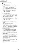
+115V DC REGULATOR Adjustment
The +115V DC Adj. control (R721) is adjusted at the
factory. However, should readjustment be required,
proceed as follows:
1. Actuate the receiver with 220V AC input voltage.
2. Select a local channel.
3. Connect positive lead of Digital Voltmeter to R603
TP751 (positive side) on PWB-A; negative lead to
chassis ground.
4. Adjust R721 to obtain a +115V DC reading.
CAUTION:
The reading should be 115V –1VDC
to ensure normal function and circuitry
reliability.
Summary of Contents for 20AR20
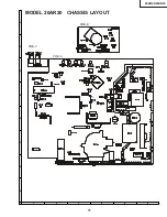
Page 11: ...11 20AR20 20AR30 6 5 4 3 2 1 A B C D E F G H MODEL 20AR20 CHASSIS LAYOUT PWB C PWB B PWB A ...
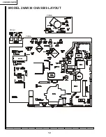
Page 12: ...12 20AR20 20AR30 6 5 4 3 2 1 A B C D E F G H MODEL 20AR30 CHASSIS LAYOUT PWB C PWB A PWB B ...
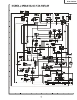
Page 13: ...13 20AR20 20AR30 6 5 4 3 2 1 A B C D E F G H MODEL 20AR20 BLOCK DIAGRAM ...
Page 14: ...14 20AR20 20AR30 6 5 4 3 2 1 A B C D E F G H MODEL 20AR30 BLOCK DIAGRAM ...
Page 17: ...17 20AR20 20AR30 6 5 4 3 2 1 A B C D E F G H 17 16 19 18 15 14 13 12 11 10 H0106GJ H0201PE ...
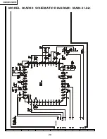
Page 20: ...20 20AR20 20AR30 6 5 4 3 2 1 A B C D E F G H MODEL 20AR30 SCHEMATIC DIAGRAM MAIN 2 Unit ...
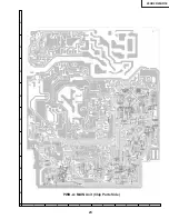
Page 23: ...23 20AR20 20AR30 6 5 4 3 2 1 A B C D E F G H PWB A MAIN Unit Chip Parts Side ...


