background image

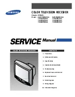
SERVICE MANUAL

COLOR TELEVISION

DOCUMENT CREATED IN JAPAN, March, 2006 GREEN

19A26C

FILE NO. 050-200613GR

(MFR’S VERSION A)

The above model is classified as a green product (*1), as indicated by the underlined serial number.

This Service Manual describes replacement parts for the green product. When repairing this green

product, use the part(s) described in this manual and lead-free solder (*2).

For (*1) and (*2), see the next page.

Summary of Contents for 19A26C

Page 1: ...R S VERSION A The above model is classified as a green product 1 as indicated by the underlined serial number This Service Manual describes replacement parts for the green product When repairing this green product use the part s described in this manual and lead free solder 2 For 1 and 2 see the next page ...

Page 2: ...nt of parts is not only confined to manufacture The same green parts used in manufacture must also be used as replacement parts 2 LEAD FREE SOLDER This product is manufactured using lead free solder as a part of a movement within the consumer products industry at large to be environmentally responsible Lead free solder must be used in the servicing and repair of this product WARNING This product i...

Page 3: ...should be used the part which has the same character Especially as to the important parts for safety which is indicated in the circuit diagram or the table of parts as a mark the designated parts must be used 4 PUT PARTS AND WIRES IN THE ORIGINAL POSITION AFTER ASSEMBLING OR WIRING There are parts which use the insulation material such as a tube or tape for safety or which are assembled in the con...

Page 4: ...E MODE LIST CONFIRMATION OF HOURS USED WHEN REPLACING EEPROM MEMORY IC ELECTRICAL ADJUSTMENTS BLOCK DIAGRAM PRINTED CIRCUIT BOARDS MAIN CRT SCHEMATIC DIAGRAMS MICON CHROMA TUNER TV POWER DEFLECTION CRT SOUND AV WAVEFORMS MECHANICAL EXPLODED VIEW MECHANICAL REPLACEMENT PARTS LIST ELECTRICAL REPLACEMENT PARTS LIST A1 1 A1 1 A1 2 A1 2 A1 2 A2 1 A3 1 A3 5 B1 1 B2 1 B2 2 C 1 C 1 C 1 D 1 D 5 E 1 E 2 F 1...

Page 5: ...uner Receive CH Destination USA W CATV 2 69 4A A 5 A 1 CH Coverage A I J W W 1 W 84 Intermediate Picture FP 45 75MHz Frequency Sound FS 41 25MHz FP FS 4 50MHz Preset CH No Stereo Dual TV Sound No Tuner Sound Muting Yes G 3 Power Power Source AC 120V AC 60Hz DC Power Consumption at AC 73 W at AC 120 V 60 Hz Stand by at AC 3 W at AC 120 V 60 Hz Per Year kWh Year Protector Power Fuse Yes G 4 Regulati...

Page 6: ...bel No Favorite CH No Color Stream DVD DTV No Control Level Yes Volume Yes Brightness Yes Contrast Yes Color Yes Tint Yes Sharpness Yes Tuning No Bass No Treble No Balance No Back Light No Stereo Audio Output SAP No Video Yes Color Stream No Channel TV Cable Yes CH Label No Game Timer Yes Sleep Timer Yes Sound Mute Yes V chip Rating No G 8 OSD Language English French Spanish G 9 Clock and Sleep Ti...

Page 7: ...5 Yes 6 Yes 7 Yes 8 Yes 9 Yes 0 Yes 100 No CH Up Yes CH Down Yes Volume Up Yes Volume Down Yes TV Caption Text Yes CH1 CH2 Yes TV Video TV AV Yes CH RTN CH ENT Quick View Yes Sleep Yes RE Call Call Yes Reset Yes Menu Yes Enter Yes Mute Yes Exit No MTS Audio Select No Set Yes Set Yes Multi Brand Keys CH Up VCR No CH Down VCR No Pause Still No TV VCR VCR No Code No FF No Rew No Rec No Play No Stop N...

Page 8: ... Max Time 120 Min Yes Stable Sound No Energy Star No Power On Memory Yes Favorite CH No G 12 Accessories Owner s Manual Language English French W Warranty Yes Remote Control Unit Yes Rod Antenna No Poles Terminal Loop Antenna No Terminal U V Mixer No DC Car Cord Center No Guarantee Card No Warning Sheet No Circuit Diagram No Antenna Change Plug No Service Facility List No Important Safety Instruct...

Page 9: ...Ext Speaker No DC Jack 12V Center No VHF UHF Antenna Input F Type AC Outlet No G 14 Set Size Approx W x D x H mm 488 x 465 x 416 G 15 Weight Net Approx 17 5kg 38 6 lbs Gross Approx 20 0kg 44 1lbs G 16 Carton Master Carton No Content Sets Material Dimensions W x D x H mm x x Description of Origin No Gift Box Material Double Brown Dimensions W x D x H mm 546 x 526 x 472 Description of Origin Yes Dro...

Page 10: ...ed Flip up the sides of the Rubber Cap in the direction of the arrow and remove one side of the support Refer to Fig 1 2 2 DISASSEMBLY INSTRUCTIONS GND on the CRT Screwdriver Alligator Clip Support CRT GND on the CRT Rubber Cap CRT Support Fig 1 1 Fig 1 2 3 After one side is removed pull in the opposite direction to remove the other NOTE Take care not to damage the Rubber Cap INSTALLATION 1 Clean ...

Page 11: ...using a blower type IC desoldering machine Refer to Fig 2 2 2 Fig 2 2 NOTE Do not add the rotating and the back and forth directions force on the IC until IC can move back and forth easily after desoldering the IC leads completely When IC starts moving back and forth easily after desoldering completely pickup the corner of the IC using a tweezers and remove the IC by moving with the IC desoldering...

Page 12: ...2 8 Thin tip Soldering Iron NOTE When the IC leads are bent during soldering and or repairing do not repair the bending of leads If the bending of leads are repaired the pattern may be damaged So always be sure to replace the IC in this case Finally confirm the soldering status on four sides of the IC using a magnifying glass Confirm that no abnormality is found on the soldering position and insta...

Page 13: ...16 x hundreds digit value 16 x tens digit value ones digit value ADDRESS DATA INIT 00 D0 CRT ON 0010 WHEN REPLACING EEPROM MEMORY IC If a service repair is undertaken where it has been required to change the MEMORY IC the following steps should be taken to ensure correct data settings while making reference to TABLE 1 Table 1 9 2 INI 0 1 3 4 5 6 7 00 8 A 57 B3 24 69 38 00 00 D0 04 EB 4E B C D E F ...

Page 14: ... press the channel button 01 on the remote control to select CUT OFF Adjust the Screen Volume until a dim raster is obtained 2 2 FOCUS 1 2 3 Receive the monoscope pattern Turn the Focus Volume fully counterclockwise once Adjust the Focus Volume until picture is distinct FUNCTION OSD H CUT OFF H VCO H PHASE V SIZE V SHIFT R DRIVE B DRIVE R BIAS G BIAS B BIAS BRIGHT CENT BRIGHT MAX BRIGHT MIN CONTRA...

Page 15: ...es minimum Refer to Fig 2 4 2 5 TINT 1 2 3 4 5 6 Receive the color bar pattern RF Input Connect the oscilloscope to TP023 Activate the adjustment mode display of Fig 1 1 and press the channel button 22 on the remote control to select TINT Press the VOL UP DOWN button on the remote control until the section A becomes as straight line Refer to Fig 2 1 Receive the color bar pattern Audio Video Input ...

Page 16: ...he remote to set to the AV mode Activate the adjustment mode display of Fig 1 1 press the channel button 17 on the remote control to select CONT MAX Press the VOL UP DOWN button on the remote control until the contrast step No becomes 77 2 12 Confirmation of Fixed Value Step No Please check if the fixed values of the each adjustment items are set correctly referring below NO 04 14 15 16 18 20 21 2...

Page 17: ...h the color bar generator from the green raster pattern to the crosshatch pattern Combine red and blue of the 3 color crosshatch pattern on the center of the screen by adjusting the pair of 4 pole magnets Combine red blue magenta and green by adjusting the pair of 6 pole magnets Adjust the crosshatch pattern to change to white by repeating steps 6 and 7 Turn the unit on and let it warm up for at l...

Page 18: ...CTRICAL ADJUSTMENT PARTS LOCATION GUIDE WIRING CONNECTION CRT PCB MAIN PCB CP803A CRT CP502 L503 S501A S501B CD501 AC IN CD101A CD101B SPEAKER CP802A CP802B TP023 TP022 R 8 0 7 R 8 0 3 CP401 C R T CP806 CP801 CRT CD801 CP803B D 5 ...

Page 19: ...T ROM RAM 38 37 57 58 16 Hor Proc SYNC SEPA Hor VCO Hor COUNT DOWN AFC 1 H COINCIDENT AFC 2 H PHASE 1 DY Q507 FEED BACK T502 4 8 13 Q502 BUFFER 6 MEMORY IC IC199 BR24L02F WE2 POWER VOL DOWN CH DOWN VOL UP CH UP X601 3 579545MHz OS101 1 16 MICON CHROMA IC IC101 OEC7091C Chroma Proc ACC C BPF APC KILLER TINT DEMO IC501 PS2561AL1 1 V W TU001 17 66 Q501 SWITCHING D501 D504 RECTIFIER Q506 SW 56 62 6 5 ...

Page 20: ...14 C410_1 R427 D501 HS402 R520 C509 R506 R503 Q502 Q501 R542 D503 D502 CP502 D408 D405 B504 B501 R 5 1 7 _ 1 D504 R422 D510 D513 D505 D506 R407 D410 R410 AFC H S401 C123_1 OS101 J 8 0 1 COL B 8V ABL GND 25V 12V 180V HEATER R423 R538 W004 R 8 0 5 R 8 0 7 D411 C434 RY501 Q507 D517 W041 R417 C516 R525 Q503 W061 C507 D514 R523 R527 R607 W046 D521 C622 W073 C610_1 W064 W062 C617 W816 W032 R405 C809 D40...

Page 21: ... R128 R126 R101 R143_1 R1008 R420 R419 C501 R532 R531 C603 R104 C108_1 C107 C105 R102 R103 R125 R609 R115 C001 R1005 R1004 R127 R116_1 R627 R124 R106_1 R105_1 R107 R108 R129 IC199 C1001 Q505 Q607 Q506 C510 R516_1 C612 C614 R701 C616 C615 R134_1 C513_1 C004_1 PRINTED CIRCUIT BOARDS MAIN CHIP MOUNTED PARTS SOLDER SIDE F 3 F 4 ...

Page 22: ...2 13 14 15 16 17 18 19 2 20 21 3 4 5 6 7 8 9 D106_1 SLR 342VCT32 POWER ON ON TIMER S802Y S802X GND B Vout OS101 ROM V3138SY 1 2 3 P CON 5V P CON 5V H_OUT H_CTL ABCL CLAMP H_CTL G OUT R OUT H_SYNC B OUT DEGAUSS_H P CON B V_OUT GND V_FEEDBACK AT 5V ABCL H_OUT X RAY SDA R OUT G OUT SCL B OUT H_SYNC AFT UNREG 12V KEY1 V_OUT POWER_FAIL UNREG 12V KEY2 V_FEEDBACK X RAY GND POWER_ON DEGAUSS_H REMOCON AT 5...

Page 23: ... 001 500V B C505 0 33 275V ECQUL C526 220 200V YK C511 1 50V KA C507 10 100V MHE R516_1 10K R537 100K 1 4W R527 5 6K 1 4W R506 2 7K 1 4W R520 12K 1 4W R509 220 1 4W R500 2 7M 1 2W 10 R512 1K 1 4W R504 100 1 4W R523 47K 1 4W R538 1 5M 1 2W R503 100 1 4W R532 10K R531 10K R502 1K 1 4W R513 2 2K 1 4W R515 120K 1 2W R519 1K 1 4W R507 100 1 4W R510 1 2M 1 2W R505 1K 1 4W R522 1 2M 1 2W R508 220 1 2W OF...

Page 24: ...07 3 9 1 2W R422 3 9 1 2W R419 680 R418 22K 1 4W R446 470 1 2W R423 100 1 4W R424 6 8K 1 4W R802 2 7K 1 4W R804 2 7K 1 4W R811 4 7K 1 4W R809 4 7K 1 4W R403 10K 1 4W R448 680 1 2W R449 680 1 2W R427 100 1 4W R405 1K 1 4W R416 1 1 2W R415 1 8K 1 2W OF PRINTING AND SUBJECT TO CHANGE WITHOUT NOTICE NOTE THIS SCHEMATIC DIAGRAM IS THE LATEST AT THE TIME DANS LA NOMENCLATURE DES PIECES N UTILISER QUE CE...

Page 25: ...K 1 4W R1008 39K R701 68 R702 47K OF PRINTING AND SUBJECT TO CHANGE WITHOUT NOTICE NOTE THIS SCHEMATIC DIAGRAM IS THE LATEST AT THE TIME DANS LA NOMENCLATURE DES PIECES N UTILISER QUE CELLS DECRITES DANGEREUSES AN POINT DE VUE SECURITE LES PIECES REPAREES PAR UN ETANT ATTENTION SINCE THESE PARTS MARKED BY CAUTION DESCRIBED IN PARTS LIST ONLY CRITICAL FOR SAFETY USE ONES ARE W811 W807 W812 W803 IC1...

Page 26: ...t the point of the corresponding balloon number in the schematic diagram MICON CHROMA TUNER 1 0 5V 2ms div 200V 20µs div 11 1V 20µs div 7 2 20V 20µs div DEFLECTION CRT 10V 5ms div 12 3 200mV 20µs div 8 0 5V 5ms div 0 5V 5ms div 4 9 20V 20µs div 10 2V 20µs div 5 1V 20µs div ...

Page 27: ... The following waveforms were measured at the point of the corresponding balloon number in the schematic diagram SOUND AV 0 5V 1ms div 17 1V 1ms div 18 200mV 500µs div 19 20 500mV 20µs div 10V 5ms div 13 50V 20µs div 14 15 50V 20µs div ...

Page 28: ...ECHANICAL EXPLODED VIEW I 1 PCB070 MAIN PCB ASS Y 203 201 107 203 106 102 205 205 205 105 205 103 101 101A 101C 101B 101D 202 108 206 206 121 114 109 109 204 204 204 204 104 PCB110 CRT PCB ASS Y 109 109 ...

Page 29: ...MECHANICAL EXPLODED VIEW PACKING DIAGRAM I 2 117 115 118 116 111 120 TM101 116 119 113 112 110 117 ...

Page 30: ...8549 7230007398 SECURITY TAG 111 72783511 J3X00221A INSTRUCTION BOOK E F 112 72795703 791WHAA134 LIGHTRON SHEET 113 72783861 723000D330 SHEET BARCODE 114 72795594 722000A267 SHEET CSA WARNING 115 72795621 791WHAA126 FILM BAG 116 72783479 792WHAA204 PACKAGE TOP 117 72798723 792WHAA055 PACKAGE BOTTOM 118 72783866 793WCDD176 GIFT BOX 119 72783512 A3X002V975 INSTRUCTION BOOK KIT 120 72795599 JB5ND100 ...

Page 31: ...465 D97U03301B DIODE ZENER MTZJ33B T 77 D106 72795529 0021721150 LED SLR 342VCT32 D403 72783209 D2MXN40020 DIODE FAST RECOVERY 1N4002 PAN D404 72794490 D97U06R21B DIODE ZENER MTZJ6 2B T 77 D405 72795543 D2MXN49370 DIODE FAST RECOVERY 1N4937 PAN D406 72783209 D2MXN40020 DIODE FAST RECOVERY 1N4002 PAN D408 72783209 D2MXN40020 DIODE FAST RECOVERY 1N4002 PAN D409 72794488 D2WT011E10 DIODE SILICON 11E1...

Page 32: ...0504101T34 SWITCH TACT EVQ21505R SW102 72794688 0504101T34 SWITCH TACT EVQ21505R SW103 72794688 0504101T34 SWITCH TACT EVQ21505R SW104 72794688 0504101T34 SWITCH TACT EVQ21505R SW105 72794688 0504101T34 SWITCH TACT EVQ21505R P C BOARD ASSEMBLIES PCB070 72783485 A3X301Q070L PCB ASS Y CMF081B PCB110 72783486 A3X301Q110L PCB ASS Y CCF073B MISCELLANEOUS B501 72794357 024HT03553 CORE BEADS W5RH3 5X5X1 ...

Page 33: ...T W DY A48AKH13X04 X601 72783450 100BT3R537 CRYSTAL HC 49U RESISTOR RC CARBON RESISTOR CAPACITORS CC CERAMIC CAPACITOR CE ALUMI ELECTROLYTIC CAPACITOR CP POLYESTER CAPACITOR CPP POLYPROPYLENE CAPACITOR CPL PLASTIC CAPACITOR CMP METAL POLYESTER CAPACITOR CMPL METAL PLASTIC CAPACITOR CMPP METAL POLYPROPYLENE CAPACITOR J2 3 ...

Page 34: ...TOSHIBA CORPORATION 1 1 SHIBAURA 1 CHOME MINATO KU TOKYO 105 8001 JAPAN ...

Reviews: