background image

Cinterion

® 

LGA DevKit Things User Guide

2 Quickstart

25

t

lga_devkit_t_ug_v01

2020-08-20

Public / Released

Page 7 of 26

2

Quickstart

Please complete the following steps to quickly get started with your LGA DevKit. 

Mount the LGA DevKit socket onto the LGA DevKit (for details se

Section 2.1

).

Insert the fixing frame and then the module into the socket and close the retention lid by
pressing it down and turning it clockwise.

Connect the provided antenna to the SMA connector named "MAIN".

Check that the jumpers are set to their default delivery positions.

Connect your host PC to either the USB or the USB VCP connector (depending on the mod-
ule). In case of USB VCP connections, install FT232R drivers.

Set the switches PWR & ASC0 at the DevKit's lower right corner to "USB". Now, the green
"PWR" LED lights up.

Shortly press the ON button to start the module. Now, the white "ON" LED lights up

The red "ERROR" LED may indicate issues that should be corrected. For de-
tails see 

Section 4.9

.

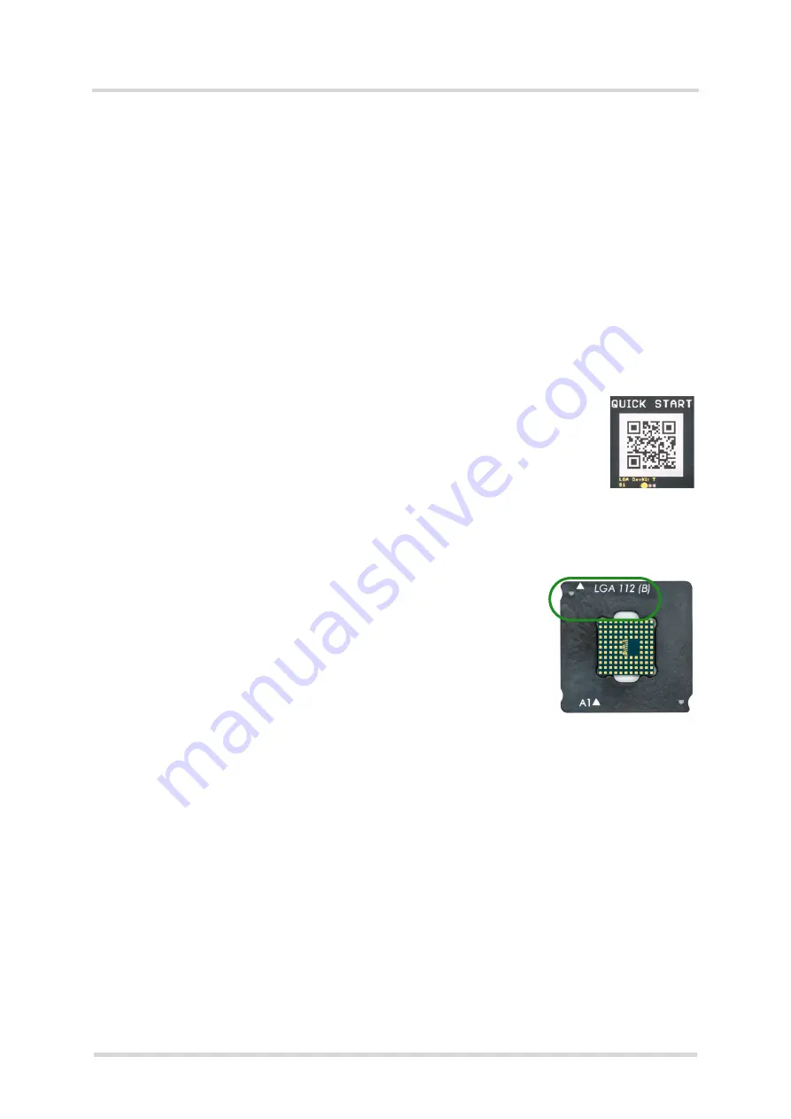
Note: By scanning the QR code at the underside of the LGA DevKit you will also
find further information, videos and available drivers.

2.1

Mounting the LGA DevKit Socket 

Before operating, the socket has to be mounted onto the LGA DevKit
with 4 screws. Scanning the QR code on the DevKit's underside and/
or the quick start guide will lead you to the DevKit's web home where
you find a short introduction and video on how to do this.

The white printing on the DevKit shows how the socket shall be orien-
tated and mounted. You can quickly adapt to different module foot-
prints by using dedicated fixing frames. All contacts have low-
resistivity needles.

Note:

 The module's thermal encapsulation inside the socket increases the thermal resistance

(Rth). Thus, you need to be aware that the board temperature may rise quite quickly until au-
tomatic thermal shutdown takes effect, especially at higher environmental temperatures or high
radio output power.

Summary of Contents for Cinterion LGA DevKit Things

Page 1: ...Cinterion LGA DevKit Things User Guide Version 01 DocId lga_devkit_t_ug_v01 ...

Page 2: ...OCUMENT THE RECIPIENT SHALL NOT COPY MODIFY DISCLOSE OR REPRODUCE THE DOCUMENT EXCEPT AS SPECIFICALLY AUTHORIZED BY THALES Copyright 2020 THALES DIS AIS Deutschland GmbH Trademark Notice Thales the Thales logo are trademarks and service marks of Thales and are registered in certain coun tries Microsoft and Windows are either registered trademarks or trademarks of Microsoft Corporation in the Unite...

Page 3: ...dule Start and Power Down 12 4 5 RST Button Module Reset 12 4 6 ASC0 Switch Module UART Interface Selection 12 4 7 PWR Switch Power Source Selection 12 4 8 Free Level Shifters 13 4 9 LEDs 13 4 10 Patch Field 14 4 11 Power Supply 15 4 11 1 Supply Current Measurement 15 4 11 2 External Reference Supply 16 5 General Characteristics 17 6 Operating the LGA DevKit with a DSB 18 6 1 LGA DevKit on DSB Min...

Page 4: ...two variants SM L please refer to the corresponding User Guide 3 The LGA DevKit T needs to be ordered together with the LGA DevKit socket T 1 1 Feature and Benefits LGA DevKit socket T supports different module footprints with different LGA pad counts for the IoT Things platform modules A LGA 68 B LGA 112 C LGA 140 Future proof ready for new upcoming modules Stand alone Get the LGA module up and r...

Page 5: ...60 N0113 A100 Base PCB for the IoT platform Things modules USB and SMA cable An ultra wideband high efficiency antenna A bag of jumpers 25pcs A quick start guide Cinterion LGA DevKit socket T Ordering number L30960 N0114 A100 The needle socket fitting on PCB version for Things Screws fixing frames retention lid Figure 1 shows the LGA DevKit package contents whereas Figure 2 shows how the LGA DevKi...

Page 6: ...vKit Things User Guide 1 3 Package Content 25 t lga_devkit_t_ug_v01 2020 08 20 Public Released Page 6 of 26 Figure 2 LGA DevKit socket T with LGA DevKit variant T Cinterion LGA DevKit socket T L30960 N0114 A100 LGA112 ...

Page 7: ...hite ON LED lights up The red ERROR LED may indicate issues that should be corrected For de tails see Section 4 9 Note By scanning the QR code at the underside of the LGA DevKit you will also find further information videos and available drivers 2 1 Mounting the LGA DevKit Socket Before operating the socket has to be mounted onto the LGA DevKit with 4 screws Scanning the QR code on the DevKit s un...

Page 8: ...e 4 show the top and bottom view of the of the LGA DevKit T variant Figure 3 LGA DevKit T top view Figure 4 LGA DevKit T bottom view Error LED Configurable interruptible signals Adjustable supply Activity LEDs Channel select Activity LED USB VCP PWR Current test USB PWR Supply mode MAIN GPS DSB interface PWR circuit CTRL Error det SIM Module footprint ex GND Patch field VCP FTDI PWR buffer ...

Page 9: ... Cinterion IoT Multifootprint Power 80Pin DSB75 DSB Mini Connector ASC0 Micro USB NativeMicro USB RF Main DRX Antenna Connector On board Sim Connector Combinded Powering MCU control unit Error detection LED Footprint detection Button ON BTN Button RST BTN USB Data Module Signals Power SIM Antenna ASC0 Signal Module Signals StatusLEDS Power User Interface Connectors Power Block Logical Block Contro...

Page 10: ...he LGA DevKit s underside you find a SIM card holder that is connected to the module s regular SIM interface lines except for the CCIN line where the default jumper needs to be set for CCIN at the CONTROL pin headers see Section 4 3 However some modules come with an additional SIM interface This can be accessed in conjunction with a DSB75 DSB Mini as port extender to support dual SIMs with the DSB...

Page 11: ...orresponds to peripherals like level shifters or the DSB connector marked green in Figure 7 Placing a jumper connects a line through a level shifter to the associated pin at the 2x40 pin connector at the underside of the LGA DevKit and thus to a connected DSB75 DSB Mini See also Figure 5 Not placing a jumper leaves a module signal open External periphery can also be connected to all accessible mod...

Page 12: ... note that this functionality is only available if the default jumper is set for EMERG_RST at the CONTROL pin block see Section 4 3 4 6 ASC0 Switch Module UART Interface Selection The ASC0 switch selects the module s UART communication interface either via USB VCP FTDI232R or via RS232 D Sub interface on the DSB75 DSB Mini Changing this from USB to RS232 during operation resets the FTDI VCP bridge...

Page 13: ...lable at the DSB connector Figure 9 Four Level shifters patch field or left edge 4 9 LEDs The LGA DevKit LEDs have the following meaning LED Meaning RED Blinking continuously Module is inserted wrongly oriented not powered insert correctly Blinking 2 times No module inserted not powered Blinking 3 times A module not supported by footprint is inserted not powered change module Lighting Overcurrent ...

Page 14: ...c here All module signals except USB and RF are accessible at the underside by the labeled pads 4 level shifters are accessible close to the patch field as well with the reference Vext and Vref The Vref related lev el shifter connections can also be accessed via four addi tional pads at the left underside of the LGA DevKit where additional pins may be soldered see Figure 9 Attention The warranty m...

Page 15: ...fer enough energy to support short 2G peak currents up to 2 5A 4 11 1 Supply Current Measurement The LGA DevKit supports three methods to measure the current consumption of the inserted module Measure the voltage across the on board 100 mOhm shunt resistor Measure the current by a current meter Power the module by an external power supply e g power analyzer All options require a jumper placed on t...

Page 16: ...cted By default i e without an external reference voltage connected the interface operates at 3V to meet the DSB75 DSB Mini requirements But if it is required to operate the interface at another voltage an external source in the range between 1 2V 5V can be connected to REF IN and GND as shown in Figure 12 Figure 12 External reference supply and pin header for free level shifter Please note that t...

Page 17: ...gs Parameter Min Max Unit Voltage on USB ports 0 3 5 5 V Voltage on DSB port 0 3 5 5 V Voltage on signal pin header depending on used module 0 3 2 1 V Current signal pin header depending on used module 10 10 mA Voltage on external reference 0 3 6 V Socket single contact continues current 2 A Table 3 Operating and environmental conditions Parameter Min Max Unit Recommended operating condition 0 45 ...

Page 18: ...lect EXT the DevKit expects the power on the DSB connector If you select USB the DevKit is powered by its USB ports and the DSB expects a separated power source Use the ASC0 switch to select the first UART If you select RS232 the modules ASC0 is conducted to the DSB and can be accessed on the D SUB connector If you select USB the UART can be accessed via USB VCP port Note that the USB VCP bridge w...

Page 19: ...A DevKit with the DSB75 please complete the following steps Mount the LGA DevKit onto the DSB75 Insert the module Set PWR and ASC0 Check if all jumpers are placed at the pin header CONTROL ASC0_A and PWR Connect the host PC to DSB75 via Sub D Connect power to DSB75 and if needed to the LGA DevKit Press the ON button or the DSB75 IGT button Figure 14 LGA DevKit on DSB75 ...

Page 20: ... compliance with the SELV require ments defined in EN 60950 1 7 4 Regulatory Compliance Information The Cinterion LGA DevKit is intended for evaluation and development purposes only and should therefore only be used in a laboratory test environment The device is not CE ap proved and has not been authorized as required by the rules of the FCC All persons handling the Cinterion LGA DevKit must be pr...

Page 21: ...0 C71 C72 C73 C74 C75 C76 C77 C78 C79 C80 C81 C82 C83 C85 C86 C87 C88 C89 CON8 D1 D2 D3 D5 IC1 IC2 IC3 IC4 IC5 IC6 IC7 IC8 IC9 IC10 IC11 I C12 IC13 IC14 IC15 IC16 IC17 IC18 IC19 IC20 IC21 IC22 IC23 IC99 JP5 L28 L29 L30 L31 L32 L33L34 L35 LED7 R1 R2 R3 R4 R5 R6 R7 R8 R9 R10 R11 R12 R13 R14 R15 R16 R17 R18 R19 R20 R21 R22 R23 R24 R25 R27 R28 R29 R30 R31 R32 R33 R34 R35 R36 R37 R38 R39 R40 R41 R42 R4...

Page 22: ...RFU L6 RFU L18 RFU L19 NC A4 NC A5 NC A6 NC A7 NC A8 NC A10 NC A11 NC A13 NC A14 NC A16 NC A17 NC A18 NC A19 NC A20 NC B4 NC B20 NC C4 NC C20 NC E4 NC E20 NC G4 NC G20 NC J4 NC J20 NC L4 NC L20 NC M4 NC M20 NC N4 NC N5 NC N6 NC N7 NC N12 NC N13 NC N14 NC N15 NC N16 NC N17 NC N18 NC N19 NC N20 R119 5 3 4 T22A R28 T22B 2 6 1 ANT_GPS 2 AGND 4 VMIC 4 MICN1 4 EPP1 4 EPN1 4 MICP1 4 I2CCLK 3 I2CCLK 3 I2C...

Page 23: ...R96 T15B R98 TP77 TP78 TP79 TP80 VOUT 5 VIN 1 EN 3 GND 2 BP 4 IC11 C75 C76 C77 C78 R99 LED9 R100 R101 D5 CON2 GND GND CON3 GND GND TP4 TP5 TP6 TP10 T17A 5 3 4 JP5 1 2 3 4 5 6 7 8 9 10 11 12 13 14 15 16 17 18 19 20 21 22 VOUT 5 VIN 1 EN 3 GND 2 BP 4 IC12 C1 C49 C54 C79 VOUT 5 VIN 1 EN 3 GND 2 BP 4 IC13 C80 C81 C82 C83 IC23A 1Vsim 2Vsim 1RST 2RST 1CLK 2CLK 1DAT 2DAT Vsim RST CLK DAT SEL N C C84 L4 C...

Page 24: ... R56 T5B 2 6 1 3 1 5 4 2 T10 T14A T14B R26 T11B T11A JP2 1 2 3 4 5 6 7 8 9 10 FLT 6 DVDT 1 EN UVLO 2 GND 8 2 ILM 7 IN 3 2 OUT 5 T6 3 1 5 4 2 T16 3 1 5 4 2 C57 R57 LED6 R63 IC10 IN 9 2 EN 7 GND 5 2 OUT 1 2 FB 3 SS 6 PB 4 R75 5 3 4 T1A 2 6 1 T1B R76 R77 R78 R79 R80 R81 C73 C74 D2 D1 R85 CON17 P 1 P 2 P 3 P 4 P 5 P 10 P 6 2 P 8 2 P 11 CON18 P 1 P 2 P 3 P 4 P 5 P 10 P 6 2 P 8 2 P 11 R60 R86 R90 R91 R9...

Page 25: ... 11 12 SCL 1 VSS 2 SDA 3 VCC 4 NC 5 TP52 TP53 TP54 TP55 C67 C68 C69 C70 C71 R82 C72 T3A R83 TP59 TP60 T3B R89 TP11 TP12 TP16 TP17 TP18 TP73 TP82 TP83 D4 TP33 TP56 TP58 TP84 TP85 TP86 TP87 TP88 TP89 TP90 TP91 TP92 TP93 TP94 TP95 TP96 TP97 TP98 TP99 TP101 TP102 TP103 TP104 TP105 TP106 TP107 TP108 TP109 TP110 TP111 TP112 TP113 TP114 TP115 TP116 TP117 TP118 TP119 TP120 TP121 TP122 TP123 TP124 TP125 TP...

Page 26: ...ALES DIS AIS Deutschland GmbH Werinherstrasse 81 81541 Munich Germany Thales 2020 All rights reserved Thales the Thales logo are trademarks and service marks of Thales and are registered in certain countries ...

Reviews: