Texas Instruments UCD90240EVM-704 User Manual Download Page 22

EVM Assembly Drawing and PCB Layout

www.ti.com

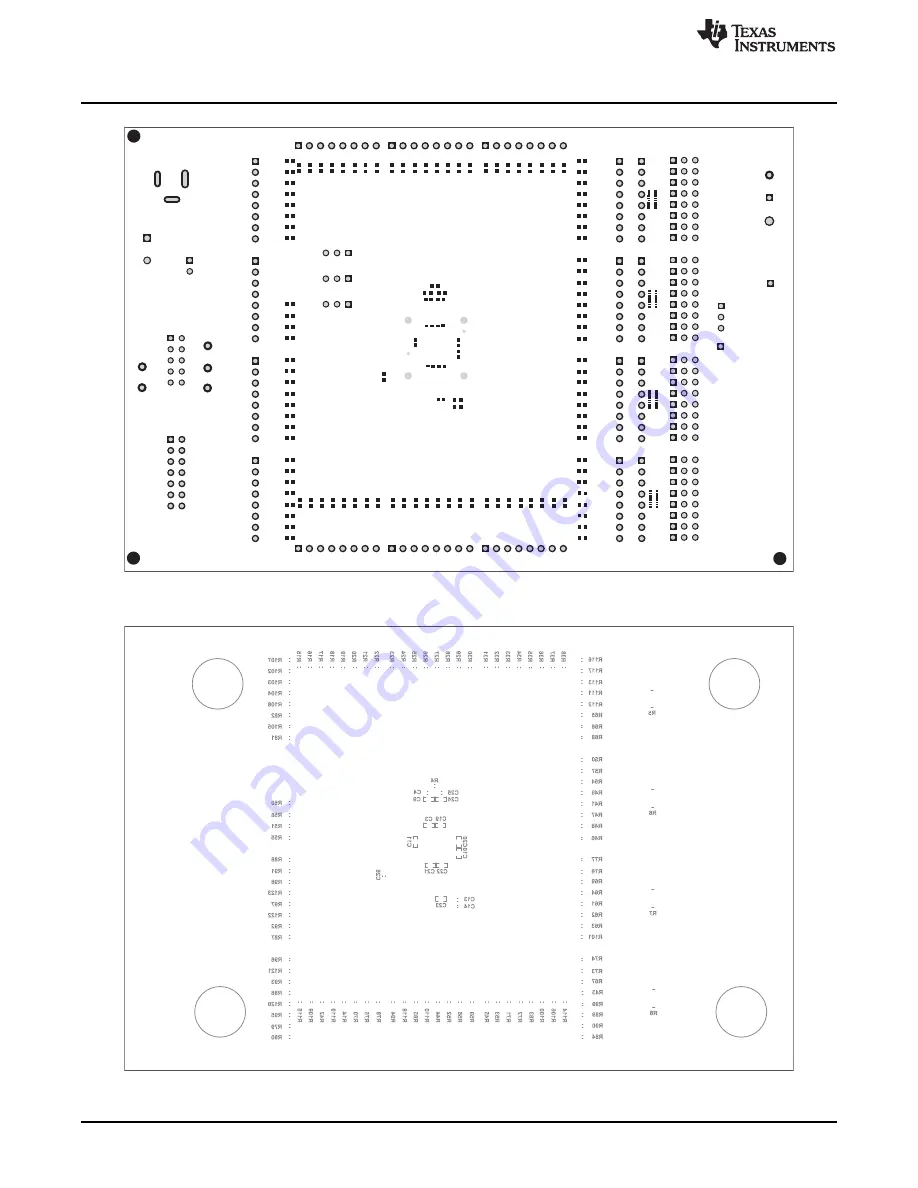
Figure 14. UCD90240EVM-704 Bottom Solder Mask

Figure 15. UCD90240EVM-704 Bottom Overlay

22

UCD90240EVM-704 24-Rail Sequencer Development Board

SLVUAF3A – March 2015 – Revised March 2015

Submit Documentation Feedback

Copyright © 2015, Texas Instruments Incorporated

Summary of Contents for UCD90240EVM-704

Page 1: ...g Example 14 7 2 Rail Enable Example 14 7 3 Fault Log Example Including Blackbox Log 14 7 4 Command GPO Example 14 7 5 Configurable Pullup Pulldown Signals 14 7 6 GPI and Logic GPO Example 14 7 7 Margin Example 15 7 8 Cascading Example 15 8 EVM Assembly Drawing and PCB Layout 16 9 Bill of Materials BOM 24 10 UCD90240EVM 704 Schematics 26 List of Figures 1 UCD90240EVM 704 Board Overview 4 2 UCD9024...

Page 2: ...es such as watchdog system reset cascading and sync clock 2 Description The UCD90240EVM 704 contains a UCD90240 sequencer device and a step down power stage using the TPS54678 synchronous step down switcher with integrated FET SWIFT Access to all of the I O pins is provided via strip connectors for integration into complex systems using clip type jumper wires The UCD90240EVM provides a PMBus power...

Page 3: ...g Input Analog input voltage range Use internal reference 0 3 3 V Analog input voltage range Use external reference 0 3 V Digital Inputs and Outputs I O high level input voltage 1 2 15 5 5 V I O low level input voltage 0 1 15 V I O input hysteresis 0 2 V I O high level output voltage Load current source 4 mA 2 4 V I O low level output voltage Load current sink 4 mA 0 4 V 1 Maximum input voltage fo...

Page 4: ...e 1 illustrates the UCD90240EVM 704 board Figure 1 UCD90240EVM 704 Board Overview 4 UCD90240EVM 704 24 Rail Sequencer Development Board SLVUAF3A March 2015 Revised March 2015 Submit Documentation Feedback Copyright 2015 Texas Instruments Incorporated ...

Page 5: ...ed PC platform Windows 7 64 bit with 8 GB RAM USB Interface Adapter EVM USB to GPIO HPA172 The latest version Fusion Digital Power Designer software can be downloaded at the following link to the Texas Instruments website http focus ti com docs toolsw folders print fusion_digital_power_designer html 5 2 Recommended Test Setup Figure 2 illustrates the recommended test setup Figure 2 UCD90240EVM 704...

Page 6: ...output J3 1 MARGIN17 Margin PWM output 2 MARGIN18 Margin PWM output 3 MARGIN19 Margin PWM output 4 MARGIN20 Margin PWM output 5 MARGIN21 Margin PWM output 6 MARGIN22 Margin PWM output 7 MARGIN23 Margin PWM output 8 MARGIN24 Margin PWM output J4 1 EN1 Rail enable output 2 EN2 Rail enable output 3 EN3 Rail enable output 4 EN4 Rail enable output 5 EN5 Rail enable output 6 EN6 Rail enable output 7 EN7...

Page 7: ...t 4 LGPO12 Logic GPO output 5 GPIO1 General Purpose I O 6 GPIO2 General Purpose I O 7 GPIO3 General Purpose I O 8 GPIO4 General Purpose I O J9 1 PMBUS_ADDR0 PMBus address pin 2 PMBUS_ADDR1 PMBus address pin 3 PMBUS_ADDR2 PMBus address pin 4 SYNC_CLOCK Sync Clock pin 5 GPIO21 General Purpose I O 6 GPIO22 General Purpose I O 7 GPIO23 General Purpose I O 8 GPIO24 General Purpose I O J10 1 GPIO13 Gene...

Page 8: ...us ALERT line 9 PMB_SCL PMBus Clock 10 PMB_SDA PMBus Data J13 1 JTAG_TMS JTAG TMS 2 JTAG nTRST unused 3 JTAG_TDI JTAG TDI 4 JTAG TDIS unused 5 JTAG VTRef unused 6 JTAG KEY 7 JTAG_TDO JTAG TDO 8 GND JTAG GND 9 JTAG RTCK unused 10 GND JTAG GND 11 JTAG_TCK JTAG TCK 12 GND JTAG GND 13 JTAG EMU0 unused 14 JTAG EMU1 unused J14 1 MON1 Analog monitor input 2 MON2 Analog monitor input 3 MON3 Analog monitor...

Page 9: ...ullup pulldown signal can be used as GPI input 8 Pullup pulldown signal can be used as GPI input J18 1 Pullup pulldown signal can be used as GPI input 2 Pullup pulldown signal can be used as GPI input 3 Pullup pulldown signal can be used as GPI input 4 Pullup pulldown signal can be used as GPI input 5 Pullup pulldown signal can be used as GPI input 6 Pullup pulldown signal can be used as GPI input...

Page 10: ...input power negative terminal J26 1 5V_VIN 5 V input power positive terminal 2 GND 5 V input power negative terminal J27 1 POL_Margin Connect this pin to a MARGIN pin to test margining function J28 1 3V3 3V3 rail connect to Pin2 to pullup 2 POL_EN POL enable 3 Input from J29 connect to Pin2 to control POL enable J29 1 Connect this pin to an EN pin to test enable function J30 1 POL_VOUT Connect thi...

Page 11: ...3 1 3V3 Connect to Pin2 to pullup 2 DIO_13 Floating pin to create a digital signal high or low 3 GND Connect to Pin2 to pulldown J44 1 3V3 Connect to Pin2 to pullup 2 DIO_14 Floating pin to create a digital signal high or low 3 GND Connect to Pin2 to pulldown J45 1 3V3 Connect to Pin2 to pullup 2 DIO_15 Floating pin to create a digital signal high or low 3 GND Connect to Pin2 to pulldown J46 1 3V3...

Page 12: ...a digital signal high or low 3 GND Connect to Pin2 to pulldown J57 1 3V3 Connect to Pin2 to pullup 2 DIO_27 Floating pin to create a digital signal high or low 3 GND Connect to Pin2 to pulldown J58 1 3V3 Connect to Pin2 to pullup 2 DIO_28 Floating pin to create a digital signal high or low 3 GND Connect to Pin2 to pulldown J59 1 3V3 Connect to Pin2 to pullup 2 DIO_29 Floating pin to create a digit...

Page 13: ...t system 6 1 Fusion Digital Power Designer Software Fusion GUI Installation Place the Fusion Digital Power Designer Software Fusion GUI Installer executable file in a known location on the host computer to be used for EVM configuration test Double click the TI Fusion Digital Power Designer 2 0 xxx exe file and proceed through the installation by accepting the installer prompts and the license agre...

Page 14: ... Blackbox Log button Adjust the external voltage applied to the MON pin such that the voltage is above OV fault threshold In the Status page Status Registers tab observe that the Vout OV Fault of the corresponding rail is raised In the Logged Faults tab observe that the Vout OV Fault of the corresponding rail is also raised In the Blackbox Info tab click Refresh Blackbox Log button Observe that th...

Page 15: ...e Sync Clock feature requires two or more UCD90240EVM 704 boards In the Fusion GUI Configure page Other Config tab configure one EVM board as Sync Clock master and all other boards as slaves Connect the multiple EVM boards to the same ground Connect all Sync Clock pins to the same node Observe that the synchronized UCD90240 devices respond to the same GPI event synchronously When the Sync Clock pi...

Page 16: ...strate the EVM assembly drawings and PCB layouts Figure 3 UCD90240EVM 704 Top Assembly Drawing Figure 4 UCD90240EVM 704 Bottom Assembly Drawing 16 UCD90240EVM 704 24 Rail Sequencer Development Board SLVUAF3A March 2015 Revised March 2015 Submit Documentation Feedback Copyright 2015 Texas Instruments Incorporated ...

Page 17: ...strates the UCD90240EVM 704 fabrication drawing Figure 5 UCD90240EVM 704 Fabrication Drawing 17 SLVUAF3A March 2015 Revised March 2015 UCD90240EVM 704 24 Rail Sequencer Development Board Submit Documentation Feedback Copyright 2015 Texas Instruments Incorporated ...

Page 18: ...te the UCD90240EVM 704 PCB drawings Figure 6 UCD90240EVM 704 Top Overlay Figure 7 UCD90240EVM 704 Top Solder Mask 18 UCD90240EVM 704 24 Rail Sequencer Development Board SLVUAF3A March 2015 Revised March 2015 Submit Documentation Feedback Copyright 2015 Texas Instruments Incorporated ...

Page 19: ...out Figure 8 UCD90240EVM 704 Top Layer Figure 9 UCD90240EVM 704 Midlayer 1 19 SLVUAF3A March 2015 Revised March 2015 UCD90240EVM 704 24 Rail Sequencer Development Board Submit Documentation Feedback Copyright 2015 Texas Instruments Incorporated ...

Page 20: ...om Figure 10 UCD90240EVM 704 Midlayer 2 Figure 11 UCD90240EVM 704 Midlayer 3 20 UCD90240EVM 704 24 Rail Sequencer Development Board SLVUAF3A March 2015 Revised March 2015 Submit Documentation Feedback Copyright 2015 Texas Instruments Incorporated ...

Page 21: ...t Figure 12 UCD90240EVM 704 Midlayer 4 Figure 13 UCD90240EVM 704 Bottom Layer 21 SLVUAF3A March 2015 Revised March 2015 UCD90240EVM 704 24 Rail Sequencer Development Board Submit Documentation Feedback Copyright 2015 Texas Instruments Incorporated ...

Page 22: ...ure 14 UCD90240EVM 704 Bottom Solder Mask Figure 15 UCD90240EVM 704 Bottom Overlay 22 UCD90240EVM 704 24 Rail Sequencer Development Board SLVUAF3A March 2015 Revised March 2015 Submit Documentation Feedback Copyright 2015 Texas Instruments Incorporated ...

Page 23: ...gure 16 UCD90240EVM 704 Drill Drawing Figure 17 UCD90240EVM 704 Board Dimensions 23 SLVUAF3A March 2015 Revised March 2015 UCD90240EVM 704 24 Rail Sequencer Development Board Submit Documentation Feedback Copyright 2015 Texas Instruments Incorporated ...

Page 24: ...14 J20 18 Header 100mil 8x1 Tin TH Header 8x1 100mil TH PEC08SAAN Sullins Connector Solutions J12 1 Header shrouded 100mil 5x2 Gold TH TH 10 Leads Body XG4C 1031 Omron Electronic 8 5x20mm Pitch 2 54mm Components J13 1 Header shrouded 100mil 7x2 Gold TH 7x2 Header N2514 6002 RB 3M J21 J23 J28 36 Header 100mil 3x1 Tin TH Header 3 PIN 100mil Tin PEC03SAAN Sullins Connector J31 J62 Solutions J24 1 Hea...

Page 25: ...Testpoint 5004 Keystone U1 1 24 Rail PMBus Power Sequencer and Power Manager ZRB0157A UCD90240ZRBR Texas Instruments UCD90240ZRBT Texas Instruments ZRB0157A U2 1 Low Noise Very Low Drift Precision Voltage Reference DGK0008A REF5030AIDGKT Texas Instruments Equivalent None 40 C to 125 C 8 pin MSOP DGK Green RoHS no Sb Br U3 1 2 95 V to 6 V Input 6 A Output 2 MHz Synchronous Step RTE0016F TPS54678RTE...

Page 26: ...een D40 MARGIN 11 MARGIN 23 MARGIN 22 GND 1 65k R85 GND 1 65k R100 GND 1 65k R106 Green D39 Green D50 Green D51 MARGIN 09 MARGIN 08 MARGIN 21 GND 1 65k R83 GND 1 65k R94 GND 1 65k R78 Green D49 Green D36 Green D37 EN22 EN23 EN24 GND 1 65k R68 GND 1 65k R65 GND 1 65k R66 Green D79 Green D78 Green D77 EN15 EN16 EN20 GND 1 65k R80 GND 1 65k R79 GND 1 65k R111 Green D27 Green D28 Green D81 EN17 GND 1 ...

Page 27: ...GND 1 65k R64 Green D62 Green D65 Green D64 Green D63 Green D59 Green D60 Green D67 Green D68 Green D58 Green D66 GPIO3 GPIO20 LGPO9 GPIO1 GND 1 65k R107 GND 1 65k R108 GND 1 65k R101 GND 1 65k R105 Green D1 Green D5 Green D61 Green D7 GPIO10 GPIO11 GPIO4 GPIO2 GPIO12 GND 1 65k R82 GND 1 65k R84 GND 1 65k R89 GND 1 65k R90 GND 1 65k R81 Green D8 Green D6 Green D53 Green D55 Green D54 LGPO1 LGPO4 L...

Page 28: ...UNUSED NC N10 UNUSED DVSS N13 PMBALERT F11 PMBUS_ADDR0 L2 PMBUS_ADDR1 L1 PMBUS_ADDR2 K1 PMBUS_CLK E10 PMBUS_CNTRL E11 PMBUS_DATA D13 U1D UCD90240ZRBR JTAG_TCK JTAG_TMS JTAG_TDO JTAG_TDI PMB_CTRL PMB_SCL TP12 TP11 PMB_CTRL PMB_SCL PMB_SDA TP10 PMB_ALERT TP13 PMB_ALERT PMBUS_ADDR2 PMBUS_ADDR1 PMBUS_ADDR0 PMB_SDA AVSS C3 AVSS E3 BPCAP D6 BPCAP J1 BPCAP J6 BPCAP K13 DVSS A1 DVSS C7 DVSS D9 DVSS E5 DVS...

Page 29: ...TMS 0 01µF C17 GND 3V3 1µF C16 GND Green D86 330 R136 GND J26 GND 5V VIN 0 R9 GND 10µF C27 4 7k R39 4 7k R40 GPIO4 GPIO5 PMB_CTRL Q2 2N7002 7 F GND Green D85 330 R133 30 1k R135 VDD Red D87 NC 1 A 2 GND 3 Y 4 VCC 5 U5 SN74LVC1G04DBVR Q1 2N7002 7 F GND 330 R2 30 1k R134 VDD PMB_ALERT GND 4 5 5 5V 1 2 J24 GND VDD GND 5 4 1 2 3 6 7 8 J1 5 4 1 2 3 6 7 8 J2 5 4 1 2 3 6 7 8 J3 5 4 1 2 3 6 7 8 J4 5 4 1 2...

Page 30: ...3 DIO_24 DIO_25 DIO_26 DIO_27 DIO_28 DIO_29 DIO_30 DIO_31 1 2 3 4 5 6 7 8 9 10 11 12 13 14 15 16 680 R6 1 2 3 J39 1 2 3 J47 1 2 3 J32 1 2 3 J33 1 2 3 J42 1 2 3 J43 1 2 3 J44 1 2 3 J37 1 2 3 J38 1 2 3 J54 1 2 3 J31 1 2 3 J55 1 2 3 J40 1 2 3 J41 1 2 3 J34 1 2 3 J35 1 2 3 J36 1 2 3 J45 1 2 3 J46 1 2 3 J48 1 2 3 J56 1 2 3 J49 1 2 3 J57 1 2 3 J50 1 2 3 J58 1 2 3 J51 1 2 3 J52 1 2 3 J59 1 2 3 J60 1 2 3 ...

Page 31: ...F C38 DNP C6 GND 500kHz 5V VIN POL_VOUT POL_Margin POL_EN To EN pin PGOOD J27 J29 J30 TP8 TP9 GND 40 2 R125 20 0k R127 22µF C29 22µF C30 22µF C31 1uH 12A L1 1 2 3 J28 100k R131 97 6k R130 1000pF C33 0 01µF C18 www ti com UCD90240EVM 704 Schematics Figure 23 UCD90240EVM Schematic 6 of 6 31 SLVUAF3A March 2015 Revised March 2015 UCD90240EVM 704 24 Rail Sequencer Development Board Submit Documentatio...

Page 32: ...trical Performance Specifications table 3 Changed typo in device name in several figure titles Corrected to UCD90240EVM 704 16 NOTE Page numbers for previous revisions may differ from page numbers in the current version 32 Revision History SLVUAF3A March 2015 Revised March 2015 Submit Documentation Feedback Copyright 2015 Texas Instruments Incorporated ...

Page 33: ...ring the warranty period to the address designated by TI and that are determined by TI not to conform to such warranty If TI elects to repair or replace such EVM TI shall have a reasonable time to repair such EVM or provide replacements Repaired EVMs shall be warranted for the remainder of the original warranty period Replaced EVMs shall be warranted for a new full ninety 90 day warranty period 3 ...

Page 34: ... by Industry Canada to operate with the antenna types listed in the user guide with the maximum permissible gain and required antenna impedance for each antenna type indicated Antenna types not included in this list having a gain greater than the maximum gain indicated for that type are strictly prohibited for use with this device Concernant les EVMs avec antennes détachables Conformément à la rég...

Page 35: ... connecting any load to the EVM output If there is uncertainty as to the load specification please contact a TI field representative During normal operation even with the inputs and outputs kept within the specified allowable ranges some circuit components may have elevated case temperatures These components include but are not limited to linear regulators switching transistors pass transistors cu...

Page 36: ...F REMOVAL OR REINSTALLATION ANCILLARY COSTS TO THE PROCUREMENT OF SUBSTITUTE GOODS OR SERVICES RETESTING OUTSIDE COMPUTER TIME LABOR COSTS LOSS OF GOODWILL LOSS OF PROFITS LOSS OF SAVINGS LOSS OF USE LOSS OF DATA OR BUSINESS INTERRUPTION NO CLAIM SUIT OR ACTION SHALL BE BROUGHT AGAINST TI MORE THAN ONE YEAR AFTER THE RELATED CAUSE OF ACTION HAS OCCURRED 8 2 Specific Limitations IN NO EVENT SHALL T...

Page 37: ...esponsible for compliance with all legal regulatory and safety related requirements concerning its products and any use of TI components in its applications notwithstanding any applications related information or support that may be provided by TI Buyer represents and agrees that it has all the necessary expertise to create and implement safeguards which anticipate dangerous consequences of failur...

Page 38: ...Mouser Electronics Authorized Distributor Click to View Pricing Inventory Delivery Lifecycle Information Texas Instruments UCD90240EVM ...

Reviews: