background image

www.ti.com

DAC and ADC GUI Configuration File Changes When Using a Xilinx Development Platform

31

SLAU580B – June 2014 – Revised September 2016

Submit Documentation Feedback

Copyright © 2014–2016, Texas Instruments Incorporated

TSW14J10 FMC-USB Interposer Card

6. Click on “Finish”.

7. Click on “Program device”. Select the device that appears.

8. Navigate to C:\

9. Select “TSW14J10_ZC706_2vp8.bit.

10. Click on “Program device”.

11. A new window will open showing the status of the programming. Once this reached 100%, the FPGA

is programmed and ready to be used with the TSW14J10 to run the HSDC Pro GUI.

Open the HSDC Pro GUI, select the

ADC

tab, then select “ADC12J4000_BYPASS” using the device drop-

down arrow. After the firmware is loaded, make sure the

Analysis Window (samples)

is no greater than

65,536 (due to the limit of the internal FPGA memory used for this capture). Next, enter "2G" in the

ADC

Output Data Rate

window.

Click the

Capture

button.

The GUI will display the new lane rate (8G) and JESD reference clock required by the capture platform
FPGA (400 MHz).

Click the

OK

button.

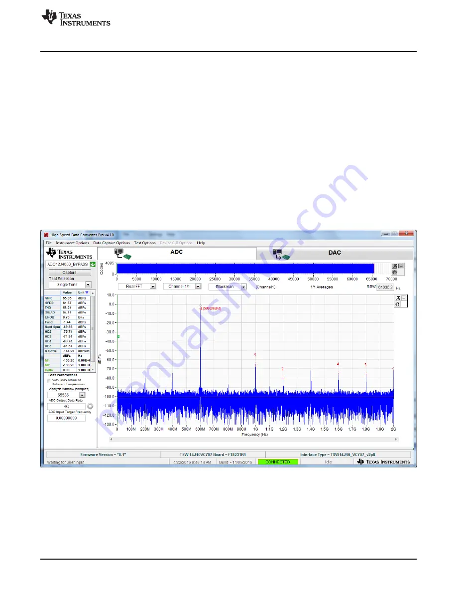
The captured results will appear as shown in

Figure 25

.

Figure 25. Captured Results for the ADC12J4000 in Bypass Mode

Summary of Contents for TSW14J10

Page 1: ...d ADC GUI Configuration File Changes When Using a Xilinx Development Platform 15 6 1 DAC38J84EVM with Xilinx VC707 Development Board Setup Example 16 6 2 ADC32RF45EVM With Xilinx VC707 Development Boa...

Page 2: ...GUI to operate as if it were connected to a TI development board The TSW14J10 is compatible with all TI ADC and DAC JESD204B based EVMs Contact FPGA vendors for other available firmware not provided b...

Page 3: ...poser Card Figure 1 TSW14J10EVM ADS42JB69EVM and Kintex KC705 Development Card The major features of the TSW14J10 are 10 transceiver lanes with speeds up to 12 5 Gbps Industry standard JTAG connector...

Page 4: ...o be used on the ADC DAC EVM due to the new height of the interface FMC connector 3 1 Power Connections The TSW14J10EVM hardware is designed to operate from a single supply voltage of 5 VDC By default...

Page 5: ...l data transmitted from Mezzanine and received by Carrier DP1_M2C_P N A2 A3 Lane 1 M C JESD Serial data transmitted from Mezzanine and received by Carrier DP2_M2C_P N A6 A7 Lane 2 M C JESD Serial data...

Page 6: ...rom carrier to mezzanine PRESENT H2 ADC DAC to FPGA EVM Present indicator ADBUS0_T C14 USB to FPGA USB SPI Interface signal ADBUS1_T C15 USB to FPGA USB SPI Interface signal ADBUS2_T H8 FPGA to USB US...

Page 7: ...by Carrier DP9_M2C_P N B4 B5 Lane 9 M C JESD Serial data transmitted from Mezzanine and received by Carrier DP0_C2M_P N C2 C3 Lane 0 C M JESD Serial data transmitted from Carrier and received by Mezz...

Page 8: ...FPGA_CLK2P N J2 J3 FPGA to DAC Spare clock FPGA_CLK1P N K4 K5 FPGA to DAC Spare clock LED_SYNC1 C18 FPGA to ADC SYNC LED indicator SPLED0 D17 FPGA to ADC Spare LED SPLED1 D18 FPGA to ADC Spare LED C19...

Page 9: ...est version of the HSDC Pro GUI slwc107x zip to a local directory on a host PC This can be found on the TI website by entering HIGH SPEED DATA CONVERTER PRO GUI INSTALLER or TSW14J10EVM in the search...

Page 10: ...e on the TI website under the High Speed Data Converter Pro Software product folder http www ti com tool dataconverterpro sw will allow the user to add these to the GUI device list After the patch has...

Page 11: ...ns displaying this value as shown in Figure 4 It is possible to connect several TSW14J10 EVMs to one host PC but the GUI can only connect to one at a time In the case where multiple boards are connect...

Page 12: ...10 USB serial converter should be located in the Hardware Device Manager under the Universal Serial Bus controllers as shown in Figure 6 This is a quad device which is why there is an A B C and D USB...

Page 13: ...nnection setup as shown in Figure 1 click on the Select ADC window in the top left of the GUI and select ADS42JB69_LMF_421 as shown in Figure 5 The GUI asks if you want to update the Firmware for the...

Page 14: ...C705 board and D3 being On on the ADS42JB69EVM Pressing the CPU reset SW7 on the KC705 board resets the JESD204B link and should synchronize the two boards After synchronization has been established e...

Page 15: ...ate is between 3 2 G and 10 3125 G Note The GTEX2 transceivers with speed grade 2 devices used on the Xilinx development platforms have a maximum rate of 10 3125 Gbps In addition the KC705 transceiver...

Page 16: ...VC707 development platform as shown in Figure 7 This example shows what must be modified in the DAC3XJ8X GUI for a setup using 4 lanes LMFS 4421 1x interpolation and a DAC sample rate of 368 64M Setu...

Page 17: ...m the DAC38J84 as follows After opening the DAC GUI enter the parameters as shown in Figure 8 Figure 8 Quick Start Menu The GUI calculates the lane rate and displays it in the box called SerDes Linera...

Page 18: ...UI the REFCLK is provided by CLKout 0 and the Core clock is provided by CLKout 12 Notice that the default setting for CLKout 12 is Group Powerdown as shown in Figure 9 Figure 9 LMK04828 Clock Outputs...

Page 19: ...x Development Platform 19 SLAU580B June 2014 Revised September 2016 Submit Documentation Feedback Copyright 2014 2016 Texas Instruments Incorporated TSW14J10 FMC USB Interposer Card The Clock Outputs...

Page 20: ...t 2 s Complement in the DAC Option window and generate a 10 MHz test tone using the IQ Multitone Generator located in the lower left of the GUI Click on the Create Tones button The display appears as...

Page 21: ...SW14J10EVM and VC707 Board The following example shows what must be modified in the ADC32RF45 GUI for a setup using the JESD204B mode setting of LMFS 82820 8 lanes 2 converters 8 octets frame 20 sampl...

Page 22: ...ab Next click on the Clock Outputs tab The GUI appears as shown in Figure 14 Figure 14 ADC32RFxx GUI LMK0828 Clock Outputs Tab For this example the lane rate is 8 Gbps Using the equation in Section 6...

Page 23: ...Outputs Tab Open HSDC Pro GUI select the ADC tab and then select ADC32RF45_LMF_82820 using the device drop down arrow After the firmware is loaded enter 32768 in the Analysis Window samples Next enter...

Page 24: ...Using a Xilinx Development Platform www ti com 24 SLAU580B June 2014 Revised September 2016 Submit Documentation Feedback Copyright 2014 2016 Texas Instruments Incorporated TSW14J10 FMC USB Interpose...

Page 25: ...platform as shown in Figure 18 Figure 18 ADC12J4000EVM TSW14J10EVM and VC707 Board The following example shows the required modifications in the ADC12J4000 GUI for a setup using the JESD204B mode set...

Page 26: ...8 input clock 2 GHz is the ADC sample clock divided by 2 to achieve the proper frequency for the reference clock this must be divided by 5 To achieve the proper core clock frequency this must be divid...

Page 27: ...le Changes When Using a Xilinx Development Platform 27 SLAU580B June 2014 Revised September 2016 Submit Documentation Feedback Copyright 2014 2016 Texas Instruments Incorporated TSW14J10 FMC USB Inter...

Page 28: ...HSDC Pro GUI select the ADC tab then select ADC12J4000_BYPASS using the device drop down arrow After the firmware is loaded make sure the Analysis Window samples is no greater than 65 536 due to the l...

Page 29: ...ent Platform 29 SLAU580B June 2014 Revised September 2016 Submit Documentation Feedback Copyright 2014 2016 Texas Instruments Incorporated TSW14J10 FMC USB Interposer Card The captured results appear...

Page 30: ...0 which will provide the reference and core clocks to the ZC706 1 Connect the TSW14J10 to the FMC HPC connector J37 on the ZC706 2 Connect the ADC to the other end of the TSW14J10 3 Connect the power...

Page 31: ...ched 100 the FPGA is programmed and ready to be used with the TSW14J10 to run the HSDC Pro GUI Open the HSDC Pro GUI select the ADC tab then select ADC12J4000_BYPASS using the device drop down arrow A...

Page 32: ...ferential signals To accommodate for this the TSW14J10EVM has options to move the SYNC signals to FMC pins H19 and H20 by making the following resistor changes 1 Remove R143 R145 2 Install 0 resistors...

Page 33: ...erter Pro 14J10ZC706 Details Firmware to C 2 Open Xilinx Vivado design tool 3 Double click on Open Hardware Manager 4 Click on Open Target 5 Select Open New Target Click on Next 6 Click on Finish 7 Cl...

Page 34: ...Figure 28 HSDC Pro GUI Click the Send button A new window opens showing the lane rate of the interface the required frequency of REFCLK as shown in Figure 29 Figure 29 HSDC Pro GUI Go back the DAC GUI...

Page 35: ...age Updated the DAC38J84EVM with Xilinx VC707 Development Board Setup Example section 16 Added the ADC32RF45EVM With Xilinx VC707 Development Board Setup Example section 21 Added the ADC12J4000EVM Wit...

Page 36: ...are returned during the warranty period to the address designated by TI and that are determined by TI not to conform to such warranty If TI elects to repair or replace such EVM TI shall have a reasona...

Page 37: ...transmitter has been approved by Industry Canada to operate with the antenna types listed in the user guide with the maximum permissible gain and required antenna impedance for each antenna type indic...

Page 38: ...ified allowable ranges some circuit components may have elevated case temperatures These components include but are not limited to linear regulators switching transistors pass transistors current sens...

Page 39: ...REMOVAL OR REINSTALLATION ANCILLARY COSTS TO THE PROCUREMENT OF SUBSTITUTE GOODS OR SERVICES RETESTING OUTSIDE COMPUTER TIME LABOR COSTS LOSS OF GOODWILL LOSS OF PROFITS LOSS OF SAVINGS LOSS OF USE L...

Page 40: ...sponsible for compliance with all legal regulatory and safety related requirements concerning its products and any use of TI components in its applications notwithstanding any applications related inf...

Page 41: ...Mouser Electronics Authorized Distributor Click to View Pricing Inventory Delivery Lifecycle Information Texas Instruments TSW14J10EVM...

Reviews: