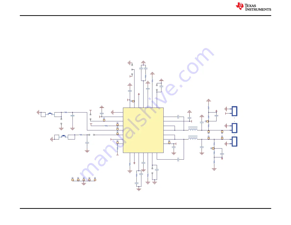
background image

3 Schematic

Figure 3-1

 illustrates the TPS65253 EVM schematic.

The resistor and capacitor values have been chosen according to the guidelines presented on the TPS65253 spec available at 

http://focus.ti.com/docs/

prod/folders/print/TPS65253.html

.

Note that for the purpose of gains-phase measurements R9 and R11 (0 Ω on the EVM) need to be replaced by suitable low value resistors as per the
network analyzer setup required. Test points are provided on either end of the resistors to allow for easy measurement. Also, R3, R4, C10, and C12 can
be populated if users desire to reduce overshoot at LX pins due to parasitic L and C resonance.

R

O

S

C

1

F

B

1

2

C

O

M

P

1

3

S

S

1

4

R

L

IM

1

5

E

N

1

6

B

S

T

1

7

VIN1

8

LX1

9

LX1

10

LX2

11

LX2

12

VIN2

13

BST2

14

E

N

2

1

5

R

L

IM

2

1

6

S

S

2

1

7

C

O

M

P

2

1

8

F

B

2

1

9

L

O

W

_

P

/S

D

A

2

0

V

7

V

2

1

V3p3

22

V3p3

23

PGOOD

24

PB

25

MR/SCL

26

LH

27

INT

28

PP

29

U1

TPS65253

3.3uF

C22

TP24

V3p3

100K

R24

0

R25

TP25

TP26

TP28

383K

R1

V7V

V3p3

100K

R28

FB1

1

0

0

p

F

D

N

I

C

3

a

20K

R3

4.7nF

C3

4

.7

n

F

C

4

1

0

0

K

R

5

JP6

4

.7

n

F

C

6

47nF

C7

TP8

10uF

C8

25V

VIN

22uF

C9

40.2K

R9a

80.6K

R9b

4.7nF

C9a

FB1

1

2

J9

4.7uH

L9

4.7uH

L11

1

2

J11

22uF
C11

40.2K

R11a

32K

R11b

4.7nF

C11a

FB2

47nF
C14

10uF

25V

C13

VIN

1

2

J8

VIN

JP15

4.7nF

C15

T

P

2

0

1

5

0

K

R

1

6

4

.7

n

F

C

1

7

1

0

0

p

F

D

N

I

C

1

8

a

2

0

K

R

1

8

4

.7

n

F

C

1

8

FB2

10uF

C21

S

D

A

0

R9

TP9

TP9a

TP9b

0

R11

TP11

TP11b

TP11a

1.8V@2A

1.2V@3A

TP1

TP2

TP3

TP4

TP5

JP20

V3p3

TP23

4.5V

V3p3

V3p3

1

2

3

4

S25

JP25

0.1uF

DNI

C25

1

2

3

4

S26

0.1uF

DNI

C26

JP23

V7V

0

R26

JP26

VOUT2

VOUT1

VIN

Figure 3-1. TPS65253 Schematic

Schematic

www.ti.com

4

TPS65253 Buck Converter Evaluation Module User's Guide

SLVU469B – JUNE 2011 – REVISED MAY 2021

Submit Document Feedback

Copyright © 2021 Texas Instruments Incorporated

Summary of Contents for TPS65253

Page 1: ...and Jumper Placement 8 5 2 Jumpers 9 5 3 Test Points and Placement 9 6 Power Up Procedure 10 7 Bill of Materials 11 8 Revision History 12 Trademarks All trademarks are the property of their respectiv...

Page 2: ...S65253 PMIC as well as the support documentation including schematic and bill of materials Introduction www ti com 2 TPS65253 Buck Converter Evaluation Module User s Guide SLVU469B JUNE 2011 REVISED M...

Page 3: ...nd Output Current Summary EVM TEST CONDITIONS OUTPUT CURRENT RANGE TPS65253EVM VIN 4 5 V to 16 V fsw 500 kHz Buck1 1 2 V 3 5 A Buck2 3 3 V 2 5 A 25 C ambient This evaluation module is designed to prov...

Page 4: ...17 COMP2 18 FB2 19 LOW_P SDA 20 V7V 21 V3p3 22 V3p3 23 PGOOD 24 PB 25 MR SCL 26 LH 27 INT 28 PP 29 U1 TPS65253 3 3uF C22 TP24 V3p3 100K R24 0 R25 TP25 TP26 TP28 383K R1 V7V V3p3 100K R28 FB1 100pF DNI...

Page 5: ...Part Placement Figure 4 2 Top Layer www ti com Placement SLVU469B JUNE 2011 REVISED MAY 2021 Submit Document Feedback TPS65253 Buck Converter Evaluation Module User s Guide 5 Copyright 2021 Texas Ins...

Page 6: ...Layer 1 Figure 4 4 Mid Layer 2 Placement www ti com 6 TPS65253 Buck Converter Evaluation Module User s Guide SLVU469B JUNE 2011 REVISED MAY 2021 Submit Document Feedback Copyright 2021 Texas Instrumen...

Page 7: ...re 4 5 Bottom Layer www ti com Placement SLVU469B JUNE 2011 REVISED MAY 2021 Submit Document Feedback TPS65253 Buck Converter Evaluation Module User s Guide 7 Copyright 2021 Texas Instruments Incorpor...

Page 8: ...Headers Description and Jumper Placement Test points Black GND White Each output feed back power good and VIN All marking on PCB Bench Test Setup Conditions www ti com 8 TPS65253 Buck Converter Evalua...

Page 9: ...asy location Close to any of these test points there are black ground test points to allow for DVM measurement or to use a metal exposed scope probe to reduce common mode noise measurements All test p...

Page 10: ...rs are powered up by the output voltages The whole start up process will take less than 100 ms PGOOD will be asserted high 32 ms after all converter outputs have reached 90 of nominal voltages 4 Apply...

Page 11: ...th Electronics 7440650022 732 1055 2 ND INDUCTOR POWER 2 2 H 6 2 A SMD 12 1 R1 383 k 603 Panasonic ECG ERJ 3EKF3833V P383KHDKR ND RES 383 k 1 10 W 1 0603 SMD 13 1 R18 10 k 603 Panasonic ECG ERJ 3EKF10...

Page 12: ...nasonic ECG ERJ 3EKF4992V P49 9KHDKR ND RES 49 9 k 1 10W 1 0603 SMD 8 Revision History NOTE Page numbers for previous revisions may differ from page numbers in the current version Changes from Revisio...

Page 13: ...ther than TI b the nonconformity resulted from User s design specifications or instructions for such EVMs or improper system design or c User has not paid on time Testing and other quality control tec...

Page 14: ...These limits are designed to provide reasonable protection against harmful interference in a residential installation This equipment generates uses and can radiate radio frequency energy and if not in...

Page 15: ...instructions set forth by Radio Law of Japan which includes but is not limited to the instructions below with respect to EVMs which for the avoidance of doubt are stated strictly for convenience and s...

Page 16: ...any interfaces electronic and or mechanical between the EVM and any human body are designed with suitable isolation and means to safely limit accessible leakage currents to minimize the risk of electr...

Page 17: ...R DAMAGES ARE CLAIMED THE EXISTENCE OF MORE THAN ONE CLAIM SHALL NOT ENLARGE OR EXTEND THIS LIMIT 9 Return Policy Except as otherwise provided TI does not offer any refunds returns or exchanges Furthe...

Page 18: ...are subject to change without notice TI grants you permission to use these resources only for development of an application that uses the TI products described in the resource Other reproduction and...

Reviews: