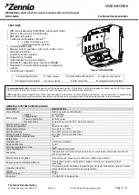
Input/Output Connections
2-2
2.1
Input/Output Connections
The TPS54980EVM−022 has the following three input/output connectors: VIN
J1, VOUT I/O J2, and VOUT CORE J3. A diagram showing the connection
points is shown in Figure 2−1. A power supply capable of supplying 8 A should
be connected to J1 through a pair of 20 AWG wires. The load should be
connected to J2 through a pair of 16 AWG wires. The maximum load current
capability should be 9 A. Wire lengths should be minimized to reduce losses
in the wires. Test point TP7 provides a place to easily connect an oscilloscope
voltage probe to monitor the output voltage. The TPS54980 is intended to be
used as a point of load regulator. In typical applications it is usually located
close to the input voltage source. When using the TPS54980EVM−022 with
an external power supply as the source for VIN, an additional bulk capacitor
may be required, depending upon the output impedance of the source and
length of the hook-up wires. The test results presented were obtained using
an additional 470-
µ
F, 16-V input capacitor. Alternately, C1 may be populated
with an input filter capacitor. Connection is shown for no load on the I/O voltage
output. The I/O voltage may supply up to 1.5 A into an external load.
Figure 2−1. Connection Diagram
Summary of Contents for TPS54980EVM-022
Page 1: ...E September 2003 PMP Systems Power User s Guide SLVU090...
Page 8: ...4...
Page 14: ...1 6...
Page 29: ...Layout 3 3 Board Layout Figure 3 2 Internal Layer 2 Figure 3 3 Internal Layer 3...
Page 30: ...Layout 3 4 Figure 3 4 Bottom Side Layout looking from top side Figure 3 5 Top Side Assembly...