Texas Instruments TPS543820EVM User Manual Download Page 14

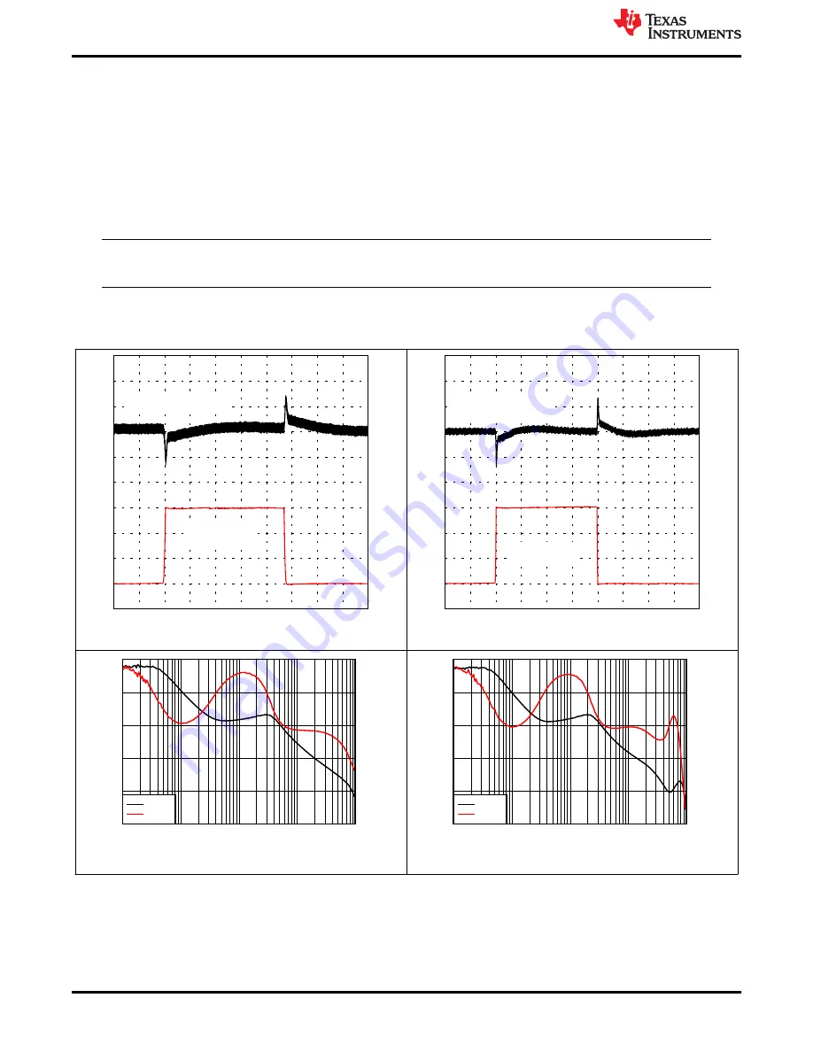
3.4 Load Transient and Loop Response

Figure 3-10

 and 

Figure 3-11

 show the response to load transients for both designs. The current step is from 1.5

A to 4.5 A and the current step slew rate is 1 A/µs. An electronic load is used to provide a DC 1.5-A load and the
load transient circuit on the EVM is used to provide a 3-A step. The VOUT voltage is measured using TP10 for
U1 and TP29 for U2.

When using the load transient circuit included on the TPS543820EVM, slowly increase amplitude of function
generator for desired load step amplitude then vary the rise and fall times for the desired slew rate. The current
for the load step can be sensed with the ISNS test point. The default resistors on the EVM provide a gain of 20
A/V. With this gain, a 3-A step will result in 150-mV at the ISNS test point.

Note

To use the load transient circuit with U1, move R27 to R28.

Figure 3-12

 and 

Figure 3-13

 show the loop characteristics for both designs. Gain and phase plots are shown for

V

IN

 voltage of 12 V and a 0.2-Ω resistive load.

Time (40 µs/div)

IOUT (1 A/div)

VOUT AC (20 mV/div)

Figure 3-10. U1 Transient Response

Time (100 µs/div)

VOUT AC (20 mV/div)

IOUT (1 A/div)

Figure 3-11. U2 Transient Response

Frequency (Hz)

G

ai

n (

dB

)

P

hase (

°)

100 200

500 1000

10000

100000

1000000

-40

-120

-20

-60

0

0

20

60

40

120

60

180

Gain
Phase

Figure 3-12. U1 Bode Plot

Frequency (Hz)

G

ai

n (

dB

)

P

hase (

°)

100 200

500 1000

10000

100000

1000000

-40

-120

-20

-60

0

0

20

60

40

120

60

180

Gain
Phase

Figure 3-13. U2 Bode Plot

Test Setup and Results

www.ti.com

14

TPS543820EVM SWIFT™ Step-Down Converter Evaluation Module User's
Guide

SLUUCE9A – DECEMBER 2020 – REVISED APRIL 2021

Submit Document Feedback

Copyright © 2021 Texas Instruments Incorporated

Summary of Contents for TPS543820EVM

Page 1: ...ipple 17 3 7 Synchronizing to a Clock 18 3 8 Start up and Shutdown with EN 19 3 9 Start up and Shutdown with VIN 20 3 10 Start up Into Pre Bias 21 3 11 Hiccup Current Limit 22 3 12 Overvoltage Protect...

Page 2: ...tion 24 Figure 3 39 U2 OVP and Recover 24 Figure 3 40 U1 Thermal Performance 8 A Load and U2 off 25 Figure 3 41 U2 Thermal Performance 8 A Load and U1 off 25 Figure 3 42 U1 Thermal Performance Both 8...

Page 3: ...0 mm2 The second design is designed to demonstrate the high efficiency that can be achieved when designing with the TPS543820 regulator The second design also includes jumpers that can be used to easi...

Page 4: ...5 V Output current range VIN 4 V to 13 2 V 0 8 A Line and load regulation VIN 4 V to 13 2 V IO 0 A to 8 A 0 1 0 3 Load transient response IO 1 5 A to 4 5 A Voltage change 25 mV Recovery time to within...

Page 5: ...5 A to 1 5 A Voltage change 25 mV Recovery time to within 0 5 60 s Loop bandwidth RO 0 2 J18 short pins 3 and 4 140 kHz Phase margin 56 degrees Input ripple voltage IO 6 A 90 mVPP Output ripple volta...

Page 6: ...After changing R7 the feedfoward capacitor C8 can also need to be changed OUT FBT FBB REF V R R 1 V u 1 In the U2 design there are a few ways to set the output voltage First jumper J14 can be used to...

Page 7: ...3 If the desired option is not available change one of the resistors to the value which sets the desired option In the U1 design change the MODE resistor to the value which sets the desired option Tab...

Page 8: ...connection With the maximum current limit setting the maximum load current capability is near 11 A before the TPS543820 goes into current limit Wire lengths must be minimized to reduce losses in the...

Page 9: ...r to connect enable divider to U2 Remove shunt to float EN pin of U2 to use internal UVLO to enable U2 J14 VOUT Select U2 VOUT selection header Use shunt to set output voltage See Table 2 1 J15 ENSYNC...

Page 10: ...plot measurements TP23 EN_U2 U2 EN test point If you are applying an external voltage it must be kept below the absolute maximum voltage of the EN pin of 6 V TP24 VO_ADJ U2 Test point for injecting cu...

Page 11: ...0 and the efficiency measurement will include the power lost in this external resistance Remove the shunts from J11 and J13 as a small amount of power is dissipated in the EN resistor divider connecte...

Page 12: ...Voltages VIN 12 V VOUT 1 V Figure 3 4 U2 Efficiency 1 V Output with Different Switching Frequencies VIN 12 V VOUT 1 8 V Figure 3 5 U2 Efficiency 1 8 V Output with Different Switching Frequencies Test...

Page 13: ...tion for U2 Figure 3 6 U1 Load Regulation Figure 3 7 U1 Line Regulation Figure 3 8 U2 Load Regulation Figure 3 9 U2 Line Regulation www ti com Test Setup and Results SLUUCE9A DECEMBER 2020 REVISED APR...

Page 14: ...gain a 3 A step will result in 150 mV at the ISNS test point Note To use the load transient circuit with U1 move R27 to R28 Figure 3 12 and Figure 3 13 show the loop characteristics for both designs G...

Page 15: ...in with Different Ramp Settings Frequency Hz Phase 100 200 5001000 10000 100000 1000000 120 90 60 30 0 30 60 90 120 150 180 Ramp 4 pF Ramp 2 pF Ramp 1 pF Figure 3 15 U2 Loop Phase with Different Ramp...

Page 16: ...Ripple No Load Time 1 s div VOUT AC 10 mV div SW 5 V div Figure 3 17 U1 Output Ripple 6 A Load Time 1 s div VOUT AC 10 mV div SW 5 V div Figure 3 18 U2 Output Ripple No Load Time 1 s div VOUT AC 10 m...

Page 17: ...U1 Input Ripple No Load Time 1 s div VIN AC 50 mV div SW 5 V div Figure 3 21 U1 Input Ripple 6 A Load Time 1 s div VIN AC 10 mV div SW 5 V div Figure 3 22 U2 Input Ripple No Load Time 1 s div VIN AC...

Page 18: ...egins synchronizing to the clock After the clock goes away the TPS543820 switches at 70 of the internal clock frequency for four pulses then transitions back to the normal internal clock frequency The...

Page 19: ...d U2 respectively When the shunt is removed from ENOFF_U1 EN is released and the start up sequence begins for U1 When the shunt is placed on RDIV_VIN EN is pulled to the input voltage through the resi...

Page 20: ...ve UVLO threshold The rate at which VIN ramps down changes as soon as the TPS543820 is disabled because it is no longer loading the input supply Time 400 s div VOUT 500 mV div VIN 10 V div EN 2 V div...

Page 21: ...t voltage does not fully discharge before EN goes high again Time 400 s div VOUT 500 mV div SW 10 V div EN 2 V div PGOOD 5 V div Figure 3 32 U2 Start up Into 0 5 V Pre Bias www ti com Test Setup and R...

Page 22: ...cale The TPS543820 tries to restart after the Hiccup wait time period but the overload was still present on the output In the next restart attempt the overload has been removed so the TPS543820 starts...

Page 23: ...ver High Limit www ti com Test Setup and Results SLUUCE9A DECEMBER 2020 REVISED APRIL 2021 Submit Document Feedback TPS543820EVM SWIFT Step Down Converter Evaluation Module User s Guide 23 Copyright 2...

Page 24: ...mpts to restart immediately after the OVP fault is cleared It does not wait for the hiccup time period Time 10 s div VOUT 500 mV div SW 10 V div VOADJ 2 V div IL 5 A div Figure 3 38 U2 Overvoltage Pro...

Page 25: ...time was used before taking each measurement Figure 3 40 U1 Thermal Performance 8 A Load and U2 off Figure 3 41 U2 Thermal Performance 8 A Load and U1 off Figure 3 42 U1 Thermal Performance Both 8 A L...

Page 26: ...ins of the IC to help maximize the thermal performance Each TPS543820 circuit has its own dedicated ground are for quiet analog ground that is connected to the main power ground plane at a single poin...

Page 27: ...atic and Bill of Materials This section presents the TPS543820EVM schematic and bill of materials www ti com Schematic and Bill of Materials SLUUCE9A DECEMBER 2020 REVISED APRIL 2021 Submit Document F...

Page 28: ...R1 EN_U1 VIN_U1 PGOOD_U1 BP5_U1 Input 4 V to 18 V Output 1 0 V at 8 A TP5 PGND_EFF_U1 NT2 Net Tie VO_SNS_U1 VOUT_U1 0 R3 TP3 SW_U1 VIN 8 VIN 12 SW 10 SW 13 BOOT 14 BP5 6 EN 7 FB 4 MODE 2 PGOOD 3 SYNC...

Page 29: ...6 EN 7 FB 4 MODE 2 PGOOD 3 SYNC FSEL 1 AGND 5 PGND 9 PGND 11 U2 TPS543820RPYR MODE PGND FB AGND NT6 Net Tie PGND PGND PGND SW FB EN 2 2 F C28 AGND 10k R11 TP18 PGOOD_U2 FSEL TP21 BP5_U2 AGND 6 04k R1...

Page 30: ...d 5 5mm Keystone_575 4 575 4 Keystone J14 J17 J18 3 Header 2 54mm 4x2 Gold TH Header 2 54mm 4x2 TH TSW 104 08 L D Samtec L1 1 470nH Inductor Shielded Composite 470 nH 15 5 A 0 0041 ohm AEC Q200 Grade...

Page 31: ...Red TH Red Multipurpose Testpoint 5010 Keystone TP4 TP5 TP8 TP16 TP17 TP19 TP20 TP33 8 Test Point Multipurpose Black TH Black Multipurpose Testpoint 5011 Keystone TP9 TP22 TP24 TP26 TP27 TP34 6 Test P...

Page 32: ...n Changes from Revision December 2020 to Revision A April 2021 Page Updated user s guide title 3 Revision History www ti com 32 TPS543820EVM SWIFT Step Down Converter Evaluation Module User s Guide SL...

Page 33: ...ther than TI b the nonconformity resulted from User s design specifications or instructions for such EVMs or improper system design or c User has not paid on time Testing and other quality control tec...

Page 34: ...These limits are designed to provide reasonable protection against harmful interference in a residential installation This equipment generates uses and can radiate radio frequency energy and if not in...

Page 35: ...instructions set forth by Radio Law of Japan which includes but is not limited to the instructions below with respect to EVMs which for the avoidance of doubt are stated strictly for convenience and s...

Page 36: ...any interfaces electronic and or mechanical between the EVM and any human body are designed with suitable isolation and means to safely limit accessible leakage currents to minimize the risk of electr...

Page 37: ...R DAMAGES ARE CLAIMED THE EXISTENCE OF MORE THAN ONE CLAIM SHALL NOT ENLARGE OR EXTEND THIS LIMIT 9 Return Policy Except as otherwise provided TI does not offer any refunds returns or exchanges Furthe...

Page 38: ...are subject to change without notice TI grants you permission to use these resources only for development of an application that uses the TI products described in the resource Other reproduction and...

Reviews: