background image

EVM Board Assembly Drawings and Layout

www.ti.com

14

SLVUBI8A – October 2018 – Revised March 2019

Submit Documentation Feedback

Copyright © 2018–2019, Texas Instruments Incorporated

TPS26630-33EVM: Evaluation Module for TPS2663x

3.4.8

Instructions to Evaluate the TPS26631, TPS26632 and TPS26635

1. Replace U1 with the TPS26631RGE on channel 1.

2. Replace U2 with TPS26632RGE or TPS26635RGE channel 2.

3. Follow the similar test procedure as TPS26630 for evaluation.

4

EVM Board Assembly Drawings and Layout

4.1

PCB Drawings

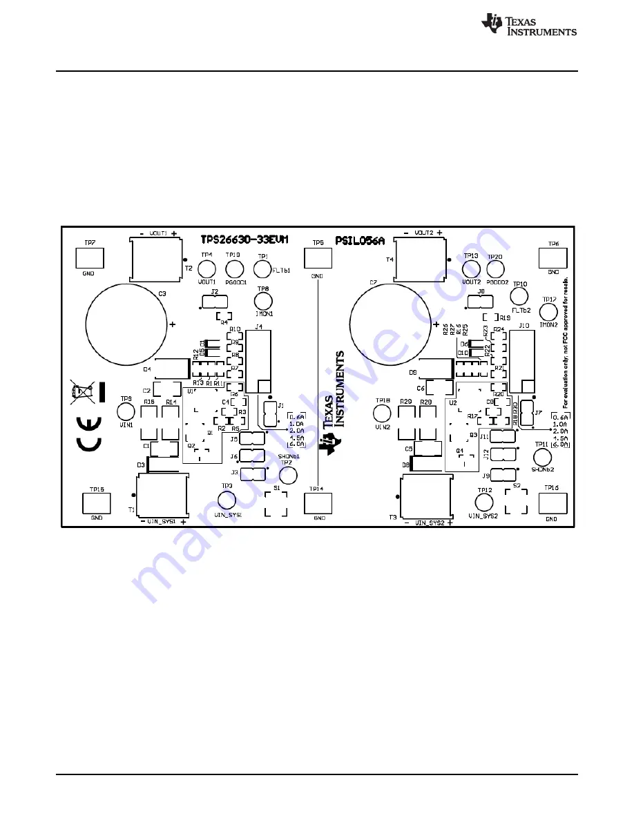
Figure 8

through

Figure 10

show component placement and layout of the EVM.

Figure 8. Top Side Placement

Summary of Contents for TPS26630-33EVM

Page 1: ... listed in Section 3 4 8 Contents 1 Introduction 2 2 Description 3 3 General Configurations 4 4 EVM Board Assembly Drawings and Layout 14 5 Schematics 16 6 Bill of Materials 17 List of Figures 1 EVM Test Setup 6 2 Output Voltage Start Up Waveform 8 3 Output Short Circuit Protection 10 4 500 V Surge Protection COUT 2 mF RLOAD 6 Ω VIN 24 V ILIM 4 5 A Peak Pulse Power 12 kW 11 5 500 V Surge Protectio...

Page 2: ... you that this EVM includes a component containing at least one substance of very high concern SVHC above 0 1 These uses from Texas Instruments do not exceed 1 ton per year The SVHC summary is listed in Table 1 Table 1 SVHC Summary Component Manufacturer Component type Component part number SVHC Substance SVHC CAS when available Diodes Inc Diode SMCJ33CA 13 F Lead 7439 92 1 1 2 EVM Features The TP...

Page 3: ...e the output connections to the load respectively Refer to the schematic in Figure 11 and EVM test setup in Figure 1 S1 and S2 allow U1 and U2 to be reset or disabled and Jumper J4 and J10 allow current limit setting to be changed S1 and S2 allows U1 and U2 to RESET A fault FLTb indicator is provided by D1 and D6 for CH1 and CH2 respectively Scaled current for each channel can be monitored at TP8 ...

Page 4: ...inuous input voltage greater than 50 V diodes D2 and D7 and capacitors C3 and C7 have to be replaced with diodes and capacitors of appropriate voltage rating Table 4 Test Points Description Channel Test Points Label Description CH1 TP1 FLTb1 CH1 fault indicator TP2 SHDNb1 CH1 shutdown input TP3 VIN_SYS1 CH1 system power supply input TP4 VOUT1 CH1 output voltage TP5 TP6 TP7 GND GND TP8 IMON1 CH1 ou...

Page 5: ...selection spacOpen position sets latch off mode spacClosed position sets auto retry mode J12 J12 CH2 PLIM setting spacDisables power limiting if installed D1 D6 RED LED Fault LED CH1 CH2 fault indicators respectively LED turns on when the internal MOSFET is disabled due to any fault condition such as undervoltage overvoltage overload short circuit reverse current and thermal shutdown D5 D10 GREEN ...

Page 6: ...bmit Documentation Feedback Copyright 2018 2019 Texas Instruments Incorporated TPS26630 33EVM Evaluation Module for TPS2663x 3 3 Test Setup Figure 1 shows the typical test setup for the TPS26630 33EVM Connect T1 T3 to the power supply and T2 T4 to the load Figure 1 EVM Test Setup ...

Page 7: ...ained Table 8 TPS26630 33EVM DMM Readings at Different Test Points Voltage test on CH1 Measured Voltage Reading Voltage test on CH2 Measured Voltage Reading VIN_SYS1 TP3 24 V 1 V DC VIN_SYS2 TP12 24 V 1 V DC VOUT1 TP4 24 V 1 V DC VOUT2 TP13 24 V 1 V DC IMON1 TP8 0 83 V 0 2 V DC IMON2 TP17 0 83 V 0 2 V DC FLTb1 TP1 22 6 V 0 5 V DC FLTb2 TP10 22 6 V 0 5 V DC SHDNb1 TP2 2 7 V 0 5 V DC SHDNb2 TP11 2 7...

Page 8: ...rt Up Time Test Follow the instructions to verify the individual channels output voltage start up time 1 Set up the oscilloscope as listed in Table 9 2 Set the load resistance to 12 Ω 1 Ω and the power supply voltage to 24 V 3 Enable the load 4 Enable the power supply and verify that the output voltage startup waveform is as shown in Figure 2 Table 9 TPS26630 33EVM Oscilloscope Setting for the Out...

Page 9: ... 2 The jumper setting for different current limits is shown in Table 10 Table 10 TPS26630 33EVM Jumper Setting for Current Limits CH1 CH2 Jumper Positions J4 J10 Load Current Limit A 1 2 6 3 4 4 5 5 6 2 7 8 1 9 10 0 6 3 Set the load resistance to 24 Ω 1 Ω and the power supply voltage to 24 V 4 Enable the load and the power supply 5 Change the load resistance to 3 Ω 1 Ω and verify that the IC limit...

Page 10: ...H2 Probe Points Channel 1 10 V div VIN_SYS1 TP3 VIN_SYS2 TP12 Channel 2 10 V div VOUT1 TP4 VOUT TP13 Channel 3 20 V div FLTb1 TP1 FLTb2 TP10 Channel 4 2 A div Input current into T1 Ve wire Input current into T3 Ve wire Trigger source Channel 1 Trigger level 12 V 1 V Trigger polarity Falling Trigger mode Single Time base 5 ms div 2 Set the current limit 2 A by installing the J4 J10 jumper in positi...

Page 11: ...load current 2 5 A Rload 10 Ω 1mF output capacitor is sufficient for supporting Class A operation 3 Set the current limit to 4 5 A or 6 A by changing jumpers J4 for CH1 4 Using the UCS 500N or similar simulator apply the surge pulse IEC 61000 4 5 Level 1 to input terminal TI of the EVM Use a 24 V DC supply for power line inputs L N of the simulator 5 Observe the waveforms for VIN1 VOUT1 IIN1 and P...

Page 12: ... 1 Set the load resistance to 4 8 Ω 0 2 Ω Rload and connect the load resistance to Terminal T2 of the EVM 2 Set the current limit to 6 A by changing jumpers J4 for CH1 3 Using the UCS 500N or similar simulator apply the EFT pulses IEC 61000 4 4 Level 3 to input terminal TI of the EVM Use a 24 V DC supply for power line inputs L N of the simulator 4 Observe the waveforms for VIN1 VOUT1 IIN1 and PGO...

Page 13: ...ch 2019 Submit Documentation Feedback Copyright 2018 2019 Texas Instruments Incorporated TPS26630 33EVM Evaluation Module for TPS2663x Figure 6 2 kV EFT Protection COUT 1 µF RLOAD 4 8 Ω VIN 24 V ILIM 6 A Figure 7 2 kV EFT Protection COUT 1 µF RLOAD 4 8 Ω VIN 24 V ILIM 6 A ...

Page 14: ...le for TPS2663x 3 4 8 Instructions to Evaluate the TPS26631 TPS26632 and TPS26635 1 Replace U1 with the TPS26631RGE on channel 1 2 Replace U2 with TPS26632RGE or TPS26635RGE channel 2 3 Follow the similar test procedure as TPS26630 for evaluation 4 EVM Board Assembly Drawings and Layout 4 1 PCB Drawings Figure 8 through Figure 10 show component placement and layout of the EVM Figure 8 Top Side Pla...

Page 15: ...Drawings and Layout 15 SLVUBI8A October 2018 Revised March 2019 Submit Documentation Feedback Copyright 2018 2019 Texas Instruments Incorporated TPS26630 33EVM Evaluation Module for TPS2663x Figure 9 Top Layer Figure 10 Bottom Layer ...

Page 16: ... C5 D9 GND 30k R24 9 09k R22 4 02k R21 3 0k R20 1 2 3 4 5 6 7 8 9 10 J10 18k R23 2 1 S2 33V D7 1000uF C7 4 7 8 1 2 3 5 6 Q3 1 2 3 Q4 887k R17 1 2 J11 30k R25 56k R27 1 2 T4 VOUT2 TP17 IMON2 49 9k R16 TP6 GND TP15 GND 100k R30 Red 1 2 D1 Red 1 2 D6 VOUT2 4 5V 60V IOUT2 0 6A 6A VIN1 VIN2 VIN2 VIN1 1uF 100V C9 DNP GND GND 1uF 100V C10 DNP TP9 VIN1 TP18 VIN2 TP19 PGOOD1 TP20 PGOOD2 0 R15 DNP 0 R14 DNP...

Page 17: ...EAR 3M 10 J1 J2 J3 J5 J6 J7 J8 J9 J11 J12 10 Header 100mil 2x1 Gold TH Sullins 100mil 1x2 230 mil above insulator PBC02SAAN Sullins Connector Solutions 11 J4 J10 2 Header 100mil 5x2 Tin TH Header 5x2 100mil Tin PEC05DAAN Sullins Connector Solutions 12 Q1 Q3 2 100 V MOSFET N CH 100 V 50 A DQG0008A VSON CLIP 8 DQG0008A CSD19537Q3 Texas Instruments 13 Q2 Q4 2 50 V MOSFET N CH 50 V 0 22 A SOT 23 SOT 2...

Page 18: ...2 SH J4 SH J7 SH J8 SH J10 6 1x2 Shunt 100mil Flash Gold Black Closed Top 100mil Shunt SPC02SYAN Sullins Connector Solutions 30 T1 T2 T3 T4 4 Terminal Block 2x1 5 08mm TH 10 16x15 2x9mm 282841 2 TE Connectivity 31 TP1 TP2 TP8 TP10 TP11 TP17 TP19 TP20 8 Test Point Multipurpose White TH White Multipurpose Testpoint 5012 Keystone 32 TP3 TP4 TP9 TP12 TP13 TP18 6 Test Point Multipurpose Red TH Red Mult...

Page 19: ...other than TI b the nonconformity resulted from User s design specifications or instructions for such EVMs or improper system design or c User has not paid on time Testing and other quality control techniques are used to the extent TI deems necessary TI does not test all parameters of each EVM User s claims against TI under this Section 2 are void if User fails to notify TI of any apparent defects...

Page 20: ... These limits are designed to provide reasonable protection against harmful interference in a residential installation This equipment generates uses and can radiate radio frequency energy and if not installed and used in accordance with the instructions may cause harmful interference to radio communications However there is no guarantee that interference will not occur in a particular installation...

Page 21: ...y for convenience and should be verified by User 1 Use EVMs in a shielded room or any other test facility as defined in the notification 173 issued by Ministry of Internal Affairs and Communications on March 28 2006 based on Sub section 1 1 of Article 6 of the Ministry s Rule for Enforcement of Radio Law of Japan 2 Use EVMs only after User obtains the license of Test Radio Station as provided in R...

Page 22: ... any interfaces electronic and or mechanical between the EVM and any human body are designed with suitable isolation and means to safely limit accessible leakage currents to minimize the risk of electrical shock hazard User assumes all responsibility and liability for any improper or unsafe handling or use of the EVM by User or its employees affiliates contractors or designees 4 4 User assumes all...

Page 23: ...OR DAMAGES ARE CLAIMED THE EXISTENCE OF MORE THAN ONE CLAIM SHALL NOT ENLARGE OR EXTEND THIS LIMIT 9 Return Policy Except as otherwise provided TI does not offer any refunds returns or exchanges Furthermore no return of EVM s will be accepted if the package has been opened and no return of the EVM s will be accepted if they are damaged or otherwise not in a resalable condition If User feels it has...

Page 24: ...se resources are subject to change without notice TI grants you permission to use these resources only for development of an application that uses the TI products described in the resource Other reproduction and display of these resources is prohibited No license is granted to any other TI intellectual property right or to any third party intellectual property right TI disclaims responsibility for...

Reviews: