www.ti.com
EVM Assembly Drawings and Layout Guidelines
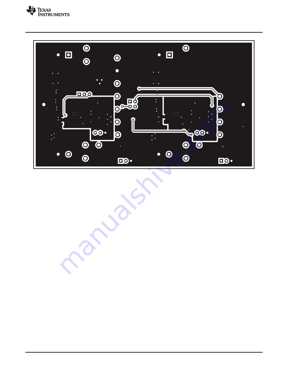
Figure 9. Bottom Side Routing Layer
13
SLVUA44 – June 2014
TPS25940XEVM-635: Evaluation Module for TPS25940X
Submit Documentation Feedback
Copyright © 2014, Texas Instruments Incorporated
Page 1: ...PS25940XEVM Schematic 3 2 EVM Test Setup 6 3 VOUT Ramp Up Time for CH1 9 4 VOUT Ramp Up Time for CH2 9 5 J4 LO Current Limit Test Auto Retry CH1 11 6 J9 No Jumper Current Limit Test with Latch CH2 11...
Page 2: ...s full evaluation of the TPS25940X devices The EVM supports two versions Auto retry and Latched of the devices on two Channels CH1 and CH2 respectively Input power is applied at J3 CH1 and J8 CH2 whil...
Page 3: ...R16 100k R17 20V D8 B320A 13 F 20V D4 B320A 13 F 330 F C10 16V D9 16V D5 4 7 F C2 4 7 F C3 4 7 F C8 4 7 F C9 DEVSLP 1 PGOOD 2 PGTH 3 OUT 4 OUT 5 OUT 6 OUT 7 OUT 8 IN 9 IN 10 IN 11 IN 12 IN 13 EN UVLO...
Page 4: ...rent 1 187 voltage on TP11 TP2 VOUT1 CH1 Output from the EVM TP9 PG1 CH1 Power good test point TP4 FLTb1 CH1 Fault test point TP12 GND GND TP13 GND GND TP14 GND GND CH2 TP15 VIN2 CH2 Input power suppl...
Page 5: ...fault current limit is 2 1 A for VIN1 J9 1 2 Install jumper at this location for 5 3 A current Limit for VIN2 2 3 Install jumper at this location for 3 6 A current Limit for VIN2 OPEN If no jumper is...
Page 6: ...T H E L P A L P H A S H I F T E N T E R R U N DG ER F I A J BK C L 7M 8N 9O DG DG DG DG T 3U 0V W X Y Z T A B U T I L I Z A T I O N H U B M A U N I C 2 B N C 4 M b s Oscilloscope xx xx xx xx x x xx x...
Page 7: ...he PWR635 assembly as shown in Figure 2 4 Ensure that the output load is disabled and the power supply is set properly for the design under test DUT Connect the negative probe of DMM to TP12 or TP25 G...
Page 8: ...green PG LED D7 turns off and red FLTb2 LED D6 turns ON Release S2 Reduce the input voltage on VIN2 and monitor VOUT2 verify that VOUT2 TP16 starts falling and is fully turned off when VIN2 TP15 reach...
Page 9: ...illustrates Figure 3 VOUT Ramp Up Time for CH1 Set the output load at 100 on CH2 and then enable the load Turn on the power supply Press the EVM RST switch S2 and release verify that VOUT2 TP16 ramps...
Page 10: ...ms div NOTE If an electronic load is used ensure that the output load is set to constant resistance mode and not constant current mode NOTE Measuring Current Limit values on the oscilloscope can easil...
Page 11: ...t the output load at 1 0 0 1 on CH2 and then enable the load Turn on the VIN2 power supply and verify that the input current is limited as per the setting in Table 10 Also verify the device is in latc...
Page 12: ...Guidelines Figure 7 through Figure 9 show component placement and layout of the EVM Figure 7 Top Side Placement Figure 8 Top Side Routing Layer 12 TPS25940XEVM 635 Evaluation Module for TPS25940X SLVU...
Page 13: ...embly Drawings and Layout Guidelines Figure 9 Bottom Side Routing Layer 13 SLVUA44 June 2014 TPS25940XEVM 635 Evaluation Module for TPS25940X Submit Documentation Feedback Copyright 2014 Texas Instrum...
Page 14: ...tivity J5 1 Header TH 100mil 2x2 Gold plated 230 mil above insulator TSW 102 07 G D TSW 102 07 G D Samtec Inc Equivalent Any LBL1 1 Thermal Transfer Printable Labels 0 650 W x 0 200 H PCB Label 0 650...
Page 15: ...t Point SMT Compact Testpoint_Keystone_Com 5016 Keystone Equivalent Any TP24 TP25 pact U1 1 2 7V 18V eFuse with True Reverse Blocking and DevSleep RVC0020A TPS25940ARVC Texas Instruments None Support...
Page 16: ...sponsible for compliance with all legal regulatory and safety related requirements concerning its products and any use of TI components in its applications notwithstanding any applications related inf...
Page 17: ...Mouser Electronics Authorized Distributor Click to View Pricing Inventory Delivery Lifecycle Information Texas Instruments TPS25940EVM 635...