background image

TMS320C6455

SPRS276M – MAY 2005 – REVISED MARCH 2012

www.ti.com

7.8.3.1

PLL Controller Divider 1 Register

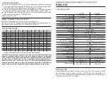
The PLL controller divider 1 register (PLLDIV1) is shown in

Figure 7-24

and described in

Table 7-33

.

31

16

Reserved

R-0

15

14

5

4

0

D1EN

Reserved

RATIO

R/W-1

R-0

R/W-1

LEGEND: R/W = Read/Write; R = Read only; -= value after reset

Figure 7-24. PLL Controller Divider 1 Register (PLLDIV1) [Hex Address: 029C 0118]

Table 7-33. PLL Controller Divider 1 Register (PLLDIV1) Field Descriptions

Bit

Field

Value

Description

31:16

Reserved

0

Reserved. The reserved bit location is always read as 0. A value written to this field has no effect.

15

D1EN

Divider D1 enable bit.

0

Divider D1 is disabled. No clock output.

1

Divider D1 is enabled.

14:5

Reserved

0

Reserved. The reserved bit location is always read as 0. A value written to this field has no effect.

4:0

RATIO

0-1Fh

Divider ratio bits.

1h

÷2. Divide frequency by 2.

4h

÷5. Divide frequency by 5.

Others

Reserved

150

C64x+ Peripheral Information and Electrical Specifications

Copyright © 2005–2012, Texas Instruments Incorporated

Submit Documentation Feedback

Product Folder Link(s):

TMS320C6455

Summary of Contents for TMS320C6455

Page 1: ... Timers Time Stamp Counter UTOPIA Enhanced Viterbi Decoder Coprocessor VCP2 UTOPIA Level 2 Slave ATM Controller Supports Over 694 7 95 Kbps AMR 8 Bit Transmit and Receive Operations up to Programmable Code Parameters 50 MHz per Direction Enhanced Turbo Decoder Coprocessor TCP2 User Defined Cell Format up to 64 Bytes Supports up to Eight 2 Mbps 3GPP 16 General Purpose I O GPIO Pins 6 Iterations Sys...

Page 2: ...00 16 bit MMACs per cycle at a 1 2 GHz clock rate the C6455 device offers cost effective solutions to high performance DSP programming challenges The C6455 DSP possesses the operational flexibility of high speed controllers and the numerical capability of array processors The C64x DSP core employs eight functional units two register files and two data paths Like the earlier C6000 devices two of th...

Page 3: ...ble as four 32 bit timers a user configurable 16 bit or 32 bit host port interface HPI16 HPI32 a peripheral component interconnect PCI a 16 pin general purpose input output port GPIO with programmable interrupt event generation modes an 10 100 1000 Ethernet media access controller EMAC which provides an efficient interface between the C6455 DSP core processor and the network a management data inpu...

Page 4: ...al L1P SRAM Cache Direct Mapped 32K Bytes L2 ROM 32K Bytes E Control Registers SPLOOP Buffer In Circuit Emulation PCI66 B UTOPIA B GPIO16 B McBSP1 A McBSP0 A SBSRAM ZBT SRAM SRAM ROM FLASH I O Devices A McBSPs Framing Chips H 100 MVIP SCSA T1 E1 AC97 Devices SPI Devices Codecs B The PCI peripheral pins are muxed with some of the HPI peripheral pins and the UTOPIA address pins For more detailed inf...

Page 5: ...LL1 and PLL1 Controller 132 3 3 Peripheral Selection After Device Reset 58 7 8 PLL2 and PLL2 Controller 147 3 4 Device State Control Registers 60 7 9 DDR2 Memory Controller 156 3 5 Device Status Register Description 71 7 10 External Memory Interface A EMIFA 158 3 6 JTAG ID JTAGID Register Description 73 7 11 I2C Peripheral 169 3 7 Pullup Pulldown Resistors 74 7 12 Host Port Interface HPI Periphera...

Page 6: ...nt in this revision Scope Applicable updates to the C64x device family specifically relating to the TMS320C6455 device have been incorporated C6455 DSP Revision History SEE ADDITIONS MODIFICATIONS DELETIONS Section 7 7 1 1 Internal Clocks and Maximum Operating Frequencies Modified values for SYSCLK2 and SYSCLK3 in fifth paragraph 6 Contents Copyright 2005 2012 Texas Instruments Incorporated Submit...

Page 7: ...uency 1 Decoder Coprocessors TCP2 clock source CPU 3 clock frequency 1 Size Bytes 2192K 32K Byte 32KB L1 Program Memory Controller SRAM Cache On Chip Memory Organization 32KB Data Memory Controller SRAM Cache 2048KB L2 Unified Memory Cache 32KB L2 ROM C64x Megamodule Megamodule Revision ID Register address location See Section 5 6 Megamodule Revision Revision ID 0181 2000h See Section 3 6 JTAG ID ...

Page 8: ...4x core through enhancements and new features Each C64x M unit can perform one of the following each clock cycle one 32 x 32 bit multiply two 16 x 16 bit multiplies two 16 x 32 bit multiplies four 8 x 8 bit multiplies four 8 x 8 bit multiplies with add operations and four 16 x 16 multiplies with add subtract capabilities including a complex multiply There is also support for Galois field multiplic...

Page 9: ...x CPU is able to detect and respond to exceptions both from internally detected sources such as illegal op codes and from system events such as a watchdog time expiration Privilege Defines user and supervisor modes of operation allowing the operating system to give a basic level of protection to sensitive resources Local memory is divided into multiple pages each with read write and execute permis...

Page 10: ... dst Á Á Á src1 Data path B Control Register 32 MSB 32 LSB dst2 A 32 MSB 32 LSB 2x 1x 32 LSB 32 MSB 32 LSB 32 MSB dst2 B B A 8 8 8 8 32 32 32 32 C C Even register file A A0 A2 A4 A30 Even register file B B0 B2 B4 B30 D D D D A On M unit dst2 is 32 MSB B On M unit dst1 is 32 LSB C On C64x CPU M unit src2 is 32 bits on C64x CPU M unit src2 is 64 bits D On L and S units odd dst connects to odd regist...

Page 11: ...including Reset Controller Registers 512 029A 0000 029A 01FF Reserved 256K 512 029A 0200 029B FFFF PLL2 Controller Registers 512 029C 0000 029C 01FF Reserved 64K 029C 0200 029C FFFF EDMA3 Channel Controller Registers 32K 02A0 0000 02A0 7FFF Reserved 96K 02A0 8000 02A1 FFFF EDMA3 Transfer Controller 0 Registers 32K 02A2 0000 02A2 7FFF EDMA3 Transfer Controller 1 Registers 32K 02A2 8000 02A2 FFFF ED...

Page 12: ... FFFF Reserved 48M 3D00 0000 3FFF FFFF PCI External Memory Space 256M 4000 0000 4FFF FFFF TCP2 Data Registers 128M 5000 0000 57FF FFFF VCP2 Data Registers 128M 5800 0000 5FFF FFFF Reserved 256M 6000 0000 6FFF FFFF EMIFA EMIF64 Configuration Registers 128M 7000 0000 77FF FFFF DDR2 Memory Controller Configuration Registers 128M 7800 0000 7FFF FFFF Reserved 256M 8000 0000 8FFF FFFF Reserved 256M 9000...

Page 13: ...alled while the remainder of the device is released During this period an external host can initialize the CPU s memory space as necessary through Host Port Interface HPI or the Peripheral Component Interconnect PCI interface Internal configuration registers such as those that control the EMIF can also be initialized by the host with two exceptions Device State Control registers Section 3 4 PLL1 a...

Page 14: ...t The destination address and length are contained within the boot table This boot mode is a software boot mode Slave I2C boot BOOTMODE 3 0 0110b A Slave I2C boot is also implemented which programs the DSP as an I2C Slave and simply waits for a Master to send data using a standard boot table format Using the Slave I2C boot a single DSP or a device acting as an I2C Master can simultaneously boot mu...

Page 15: ... level bootloader allows for any level of customization to current boot methods as well as definition of a completely customized boot TI offers a few 2nd level bootloaders such as an EMAC bootloader and a UTOPIA bootloader which can be loaded using the Master I2C boot Copyright 2005 2012 Texas Instruments Incorporated Device Overview 15 Submit Documentation Feedback Product Folder Link s TMS320C64...

Page 16: ...5 DVDD33 HD0 AD0 VSS HD11 AD11 TOUTL0 EMU3 EMU7 TOUTL1 VSS DVDD33 VSS DVDD33 VSS HDS2 PCBE1 HCNTL0 PSTOP HCS PPERR VSS HD8 AD8 VSS HD26 AD26 VSS HD7 AD7 HD1 AD1 EMU2 RSV39 VSS DVDD33 HAS PPAR HD5 AD5 AH TINPL0 EMU17 TDO NMI EMU16 GP 4 VSS TRST TDI RSV27 EMU9 AJ TINPL1 TMS VSS CLKS RSV40 GP 5 DVDD33 DVDD33 TCK RSV26 SYSCLK4 GP 1 14 VSS DVDD33 RESETSTAT POR VSS CVDD CVDD RESET DVDD33 VSS 15 AVDDA VS...

Page 17: ...ED19 DVDD33 CVDD CVDD DVDD33 VSS VSS DVDD33 DVDD33 VSS VSS VSS DVDD33 VSS AED26 VSS DVDD33 AED22 AED0 AED13 AED12 AED10 RIOTX0 AVDDT RIOTX3 AED30 DVDD33 AEA12 UTOPIA_EN VSS VSS VSS VSS RSV20 AEA0 CFGGP0 VSS DVDD33 AR W DVDD33 PCI_EN DVDD33 AED23 AAWE ASWE RIOTX1 RIOTX2 DVDD33 ABE3 AEA3 AED8 AH DVDD33 VSS AVDDT RIORX0 AED14 RIORX3 AED2 AED18 VSS RIORX0 VSS VSS VSS RIORX3 AJ VSS DVDD33 VSS RIORX1 AE...

Page 18: ...VDD18 DVDD18 AED39 DVDD33 VSS VSS RSV30 DVDD33 VSS VSS DVDD18 VSS DVDD18 DVDD18 AED35 AED48 AED54 DVDD18 VSS DVDD33 AED47 DVDD33 DVDD33 AED57 DED27 DSDDQS2 DEA0 AED41 DSDDQM3 DVDD33 VSS CVDD VSS CVDD VSS AEA8 PCI_EEAI RSV31 AED38 VSS AARDY VSS AED36 AED63 VSS DED22 DED18 DEA6 ABE5 AEA7 AED43 B DED29 DED31 DVDD18 DED25 RSV22 DEA2 AED49 AED51 VSS DVDD18 DED21 DED16 DEA7 A DED28 DED30 VSS DED24 DVDD1...

Page 19: ...0 DVDD33 VSS VSS VSS DVDD33MON VSS RSV21 DED13 DED4 VSS AVDLL1 VSS VREFHSTL RGMDCLK RSV24 DSDDQ GATE1 RGRXCTL VSS DVDD15 RGTXC RGRXC DSDDQS1 DVDD18 DVDD18 RSV14 DVDD18 URDATA7 MRXD7 VSS CVDD RSV28 CVDD URADDR4 PCBE0 GP 2 UXADDR2 PCBE3 DVDD33 UXENB MTXEN RMTXEN VSS DVDD33 VSS RGMDIO PLLV2 VSS DED11 DVDD18 DVDD18 URDATA4 MRXD4 UXADDR3 MDIO RGTXD2 B DVDD15 VSS DVDD18 DVDD18 RSV07 DVDD18 CLKIN2 DVDD33...

Page 20: ... RSV05 RSV43 RSV44 RSV42 RESETSTAT CLKIN2 POR PCI_EN Peripheral Enable Disable Clock PLL2 PLLV2 PLLV1 TMS320C6455 SPRS276M MAY 2005 REVISED MARCH 2012 www ti com 2 6 Signal Groups Description A This pin functions as GP 1 by default For more details see Section 3 Figure 2 6 CPU and Peripheral Signals 20 Device Overview Copyright 2005 2012 Texas Instruments Incorporated Submit Documentation Feedback...

Page 21: ... function as GPIO peripheral pins For more details see the section of this document Device Configuration C These UTOPIA and PCI peripheral pins are muxed with the GPIO peripheral pins and by default these signals function as GPIO peripheral pins For more details see the section of this document Device Configuration GP 7 GP 6 GP 5 GP 4 CLKX1 GP 3 B URADDR4 GP 2 PCBE0 C SYSCLK4 GP 1 A CLKR1 GP 0 B T...

Page 22: ...ontrol DDR2 Memoty Controller 32 bit Data Bus DSDCAS DSDCKE DDR2CLKOUT DSDDQS 3 0 DSDRAS DSDWE DSDDQS 3 0 ABE7 ABE6 ABE5 ABE4 ACE5 A Bank Address ABA 1 0 AR W AAOE ASOE ASADS ASRE Bank Address DBA 2 0 DEODT 1 0 DSDDQGATE 0 DSDDQM3 DSDDQM2 DSDDQM1 DSDDQM0 DSDDQGATE 1 DSDDQGATE 2 DSDDQGATE 3 TMS320C6455 SPRS276M MAY 2005 REVISED MARCH 2012 www ti com Figure 2 8 EMIFA and DDR2 Memory Controller Perip...

Page 23: ...heral By default these pins function as HPI When the HPI is enabled the number of HPI pins used depends on the HPI configuration HPI16 or HPI32 For more details on these muxed pins see the Device Configuration section of this document B These McBSP1 peripheral pins are muxed with the GPIO peripheral pins and by default these signals function as GPIO peripheral pins For more details see the Device ...

Page 24: ... the Device Configuration section of this document RGTXC RGRXC RGREFCLK UXDATA 7 2 MTXD 7 2 UXDATA 1 0 MTXD 1 0 RMTXD 1 0 Transmit RGMII A GMII RMII MII RGRXD 3 0 URDATA 7 2 MRXD 7 2 URDATA 1 0 MRXD 1 0 RMRXD 1 0 RGMII A GMII RMII MII RGMII A GMII RMII MII RGMII A GMII RMII MII RGMII A GMII RMII MII GMII RMII MII RGMII A UXCLK MTCLK RMREFCLK URCLK MRCLK UXCLAV GMTCLK Ethernet MAC EMAC TMS320C6455 ...

Page 25: ...ins or have no function For more details on these muxed pins see the Device Configuration section of this document HD 15 0 AD 15 0 HR W PCBE2 HDS2 PCBE1 UXADDR4 PCBE0 GP 2 HHWIL PCLK HINT PFRAME URADDR2 PINTA GP 14 Data Address Arbitration 32 Clock Control PCI Interface A HAS PPAR URADDR1 PRST GP 13 HRDY PIRDY HCNTL0 PSTOP UXADDR0 PTRDY UXADDR2 PCBE3 UXADDR1 PIDSEL HCNTL1 PDEVSEL HDS1 PSERR Error ...

Page 26: ... 4 AF7 I O Z IPU Emulation pin 0 EMU1 4 AE11 I O Z IPU Emulation pin 1 EMU2 AG9 I O Z IPU Emulation pin 2 EMU3 AF10 I O Z IPU Emulation pin 3 EMU4 AF9 I O Z IPU Emulation pin 4 EMU5 AE12 I O Z IPU Emulation pin 5 EMU6 AG8 I O Z IPU Emulation pin 6 EMU7 AF12 I O Z IPU Emulation pin 7 EMU8 AF11 I O Z IPU Emulation pin 8 EMU9 AH13 I O Z IPU Emulation pin 9 EMU10 AD10 I O Z IPU Emulation pin 10 EMU11 ...

Page 27: ...1 AJ13 O Z IPD CLKR1 GP 0 AF4 I O Z IPD HOST PORT INTERFACE HPI or PERIPHERAL COMPONENT INTERCONNECT PCI PCI enable pin This pin controls the selection enable disable of the HPI and GP 15 8 or PCI peripherals This pin works in conjunction with the PCI_EN Y29 I IPD MCBSP1_EN AEA5 pin to enable disable other peripherals for more details see Section 3 Device Configuration HINT PFRAME U3 I O Z Host in...

Page 28: ...ress pin 1 UXADDR1 I or PCI initialization device UXADDR1 PIDSEL R3 I select I By default this pin has no function UTOPIA transmit address pin 0 UXADDR0 I or PCI target ready PRTDY UXADDR0 PTRDY P4 I O Z I O Z By default this pin has no function HD31 AD31 AA3 HD30 AD30 AA5 HD29 AD29 AC4 HD28 AD28 AA4 HD27 AD27 AC5 HD26 AD26 Y1 HD25 AD25 AD2 HD24 AD24 W1 Host port data 31 16 pin I O Z default or PC...

Page 29: ...of external memory ABE3 AA29 O Z IPU Byte write enables for most types of memory ABE2 AA28 O Z IPU ABE1 AA25 O Z IPU ABE0 AA26 O Z IPU EMIFA 64 BIT BUS ARBITRATION AHOLDA N26 O IPU EMIFA hold request acknowledge to the host AHOLD R29 I IPU EMIFA hold request from the host ABUSREQ L27 O IPU EMIFA bus request output EMIFA 64 BIT ASYNCHRONOUS SYNCHRONOUS MEMORY CONTROL EMIFA external input clock The ...

Page 30: ...on 2 4 Boot Sequence CFGGP 2 0 pins must be set to 000b during reset for proper operation of the PCI boot mode EMIFA input clock source select Clock mode select for EMIFA AECLKIN_SEL AEA15 0 AECLKIN default mode 1 SYSCLK4 CPU x Clock Rate The SYSCLK4 clock rate is software selectable via the Software PLL1 Controller By default SYSCLK4 is selected as CPU 8 clock rate HPI peripheral bus width HPI_WI...

Page 31: ... The PCI peripheral needs be enabled PCI_EN 1 to use this function Selects the PCI operating frequency of 66 MHz or 33 MHz PCI operating frequency is selected at reset via the pullup pulldown resistor on the PCI66 pin O Z IPD AEA6 0 PCI operates at 33 MHz default 1 PCI operates at 66 MHz Note If the PCI peripheral is disabled PCI_EN 0 this pin must not be pulled up McBSP1 Enable bit MCBSP1_EN Sele...

Page 32: ... F28 AED51 B28 AED50 G27 AED49 B27 AED48 G28 AED47 H25 AED46 J26 AED45 H26 AED44 J27 AED43 H27 I O Z IPU EMIFA external data AED42 J28 AED41 C29 AED40 J29 AED39 D29 AED38 J25 AED37 F29 AED36 F26 AED35 G29 AED34 K28 AED33 K25 AED32 K27 AED31 AA27 AED30 AG29 AED29 AB29 AED28 AC27 AED27 AB28 AED26 AC26 AED25 AB27 AED24 AC25 AED23 AB26 AED22 AD28 32 Device Overview Copyright 2005 2012 Texas Instrument...

Page 33: ...O Z DDR2 Memory Controller SDRAM row address strobe DSDWE B13 O Z DDR2 Memory Controller SDRAM write enable DSDCKE D14 O Z DDR2 Memory Controller SDRAM clock enable used for self refresh mode DEODT1 A17 O Z On die termination signals to external DDR2 SDRAM These pins should not be connected to the DDR2 SDRAM Note There are no on die termination resistors implemented on the C6455 DEODT0 E16 O Z DSP...

Page 34: ...s are used to meet AC timings For more detailed information DSDDQS1 D8 I O Z see the Implementing DDR2 PCB Layout on the TMS320C6454 5 application report literature number SPRAAA7 DSDDQS0 D11 I O Z DDR2 MEMORY CONTROLLER 32 BIT ADDRESS DEA13 B15 DEA12 A15 DEA11 A16 DEA10 B16 DEA9 C16 DEA8 D16 DEA7 B17 O Z DDR2 Memory Controller external address DEA6 C17 DEA5 D17 DEA4 E17 DEA3 A18 DEA2 B18 DEA1 C18...

Page 35: ...0 DED6 C10 DED5 B10 DED4 A10 DED3 D12 DED2 C12 DED1 B12 DED0 A12 TIMER 1 TOUTL1 AG7 O Z IPD Timer 1 output pin for lower 32 bit counter TINPL1 AJ6 I IPD Timer 1 input pin for lower 32 bit counter TIMER 0 TOUTL0 AF8 O Z IPD Timer 0 output pin for lower 32 bit counter TINPL0 AH6 I IPD Timer 0 input pin for lower 32 bit counter INTER INTEGRATED CIRCUIT I2C SCL AG26 I O Z I2C clock When the I2C module...

Page 36: ... available status output signal from UTOPIA Slave 0 indicates a complete cell is NOT available for transmit UXCLAV GMTCLK K5 I O Z 1 indicates a complete cell is available for transmit When the UTOPIA peripheral is disabled UTOPIA_EN AEA12 pin 0 this pin is EMAC GMII transmit clock MACSEL 1 0 dependent UTOPIA transmit interface enable input signal Asserted by the Master ATM Controller to indicate ...

Page 37: ...al is disabled UTOPIA_EN AEA12 pin 0 this pin is EMAC MII default or GMII receive data valid MACSEL 1 0 dependent Receive Start of Cell signal This signal is output by the Master ATM Controller to indicate to the UTOPIA Slave that the first valid byte of the cell is available to URSOC MRXER sample on the 8 bit Receive Data Bus URDATA 7 0 H4 I O Z RMRXER When the UTOPIA peripheral is disabled UTOPI...

Page 38: ...on pins the MAC_SEL 1 0 AEA 10 9 pins that select one of the four interface modes MII RMII GMII or RGMII for the EMAC MDIO interface For more detailed information on the EMAC configuration pins see Section 3 Device Configuration UTOPIA receive clock URCLK driven by Master ATM Controller I or when the UTOPIA peripheral is disabled UTOPIA_EN AEA12 pin 0 this pin is URCLK MRCLK H1 I EMAC receive cloc...

Page 39: ...eference clock RMREFCLK I The EMAC function is controlled by the MACSEL 1 0 AEA 10 9 pins For more detailed information see Section 3 Device Configuration UTOPIA transmit Start of Cell signal O This signal is output by the UTOPIA Slave on the rising edge of the UXCLK indicating that the first valid byte of the cell is available on the 8 bit Transmit Data Bus UXDATA 7 0 UXSOC MCOL K3 I O Z When the...

Page 40: ...ve control I This pin is available only when RGMII mode is RGRXCTL C2 I selected MACSEL 1 0 11 RESERVED FOR TEST RSV02 V5 RSV03 W3 Reserved These pins must be connected directly to core supply CVDD for proper device operation RSV04 N11 RSV05 P11 Reserved This pin must be connected directly to 1 5 1 8 V I O supply DVDD15 for proper device operation RSV07 G4 I NOTE If the EMAC RGMII is not used thes...

Page 41: ...15 T1 VSS for proper device operation The resistor used should have a minimal rating of 1 10 W Reserved This pin must be connected via a 20 Ω resistor directly to 3 3 V I O RSV16 T2 Supply DVDD33 for proper device operation The resistor used should have a minimal rating of 1 10 W RSV17 AE21 A RSV18 E13 A RSV19 F18 A RSV20 U29 A RSV21 A6 A RSV22 B26 O RSV23 C26 O RSV24 B6 O RSV25 C6 O RSV26 AJ11 A ...

Page 42: ...n the RGMII pins see Section 7 3 4 Die side 1 8 V I O supply DVDD18 voltage monitor pin The monitor pins indicate the voltage on the die and therefore provide the best probe point for voltage monitoring purposes For more information regarding the use of this DVDD18MON A26 and other voltage monitoring pins see the TMS320C6455 Design Guide and Comparisons to TMS320TC6416T application report literatu...

Page 43: ...nd 1200 devices AVDDT AF20 A 1 2 V I O supply voltage 850 devices Do not use core supply AH20 NOTE If RapidIO is not used these pins can be connected directly to VSS AJ17 AJ23 A1 B5 1 8 V or 1 5 V I O supply voltage for the RGMII function of the EMAC NOTE If the RGMII mode of the EMAC is not used the DVDD15 VREFHSTL D2 RSV13 and RSV14 pins can be connected to directly ground VSS to save DVDD15 D5 ...

Page 44: ...E NO A29 E26 E28 G2 H23 H28 J6 J24 K1 K7 K23 L24 M7 M23 M28 N24 P6 P28 R1 R6 R23 DVDD33 T7 S 3 3 V I O supply voltage T24 U23 V1 V7 V24 W23 Y7 Y24 AA1 AA6 AA23 AB7 AB24 AC6 AC9 AC11 AC13 AC19 AC21 AC23 AC29 44 Device Overview Copyright 2005 2012 Texas Instruments Incorporated Submit Documentation Feedback Product Folder Link s TMS320C6455 ...

Page 45: ... AF24 S 3 3 V I O supply voltage AG12 AG17 AG23 AH14 AH16 AH24 AJ1 AJ7 AJ15 AJ25 AJ29 L12 L14 L16 L18 M11 M13 M15 M17 M19 N12 1 25 V core supply voltage 1000 and 1200 devices CVDD S 1 2 V core supply voltage 850 and 720 devices N14 N16 N18 P13 P15 P17 P19 R12 R14 R16 Copyright 2005 2012 Texas Instruments Incorporated Device Overview 45 Submit Documentation Feedback Product Folder Link s TMS320C645...

Page 46: ...12 1 25 V core supply voltage 1000 and 1200 devices CVDD S 1 2 V core supply voltage 850 and 720 devices U14 U18 V11 V13 V19 W12 W14 GROUND PINS A8 A11 A20 A23 B1 B29 C5 D1 E5 E7 VSS GND Ground pins E19 E25 E29 F4 F6 F8 F10 F12 F14 F16 46 Device Overview Copyright 2005 2012 Texas Instruments Incorporated Submit Documentation Feedback Product Folder Link s TMS320C6455 ...

Page 47: ...TYPE 1 IPD IPU 2 DESCRIPTION NAME NO F20 F22 F24 G1 G5 G7 G9 G11 G13 G15 G17 G19 G21 G23 H6 H24 VSS GND Ground pins H29 J7 J23 K2 K6 K24 L7 L11 L13 L15 L17 L19 L23 M6 M12 M14 Copyright 2005 2012 Texas Instruments Incorporated Device Overview 47 Submit Documentation Feedback Product Folder Link s TMS320C6455 ...

Page 48: ... IPD IPU 2 DESCRIPTION NAME NO M16 M18 M24 M26 M29 N2 N13 N15 N17 N19 N23 P7 P12 P14 P16 P18 P29 VSS GND Ground pins R2 R7 R11 R13 R15 R17 R19 R24 T6 T12 T14 T16 T18 T23 U7 U11 U13 48 Device Overview Copyright 2005 2012 Texas Instruments Incorporated Submit Documentation Feedback Product Folder Link s TMS320C6455 ...

Page 49: ...IPD IPU 2 DESCRIPTION NAME NO U15 U17 U19 U24 V2 V6 V12 V14 V16 V18 V23 W7 W11 W13 W15 W17 VSS GND Ground pins W19 W24 Y6 Y23 AA2 AA7 AA24 AB6 AB23 AC7 AC8 AC10 AC12 AC14 AC16 AC18 Copyright 2005 2012 Texas Instruments Incorporated Device Overview 49 Submit Documentation Feedback Product Folder Link s TMS320C6455 ...

Page 50: ... NAME NO AC20 AC22 AC24 AC28 AD6 AD13 AD15 AD17 AD19 AD21 AD23 AE4 AE7 AE16 AE18 AE20 AE22 AE24 VSS GND Ground pins AF2 AF19 AF21 AG13 AG16 AG20 AG24 AH1 AH15 AH19 AH21 AH25 AH29 AJ8 AJ14 AJ16 AJ20 AJ24 50 Device Overview Copyright 2005 2012 Texas Instruments Incorporated Submit Documentation Feedback Product Folder Link s TMS320C6455 ...

Page 51: ...C6455GTZ2 Texas Instruments recommends two of three possible prefix designators for its support tools TMDX and TMDS These prefixes represent evolutionary stages of product development from engineering prototypes TMX TMDX through fully qualified production devices tools TMS TMDS Device development evolutionary flow TMX Experimental device that is not necessarily representative of the final device s...

Page 52: ...port The following documents describe the TMS320C6455 Fixed Point Digital Signal Processor Copies of these documents are available on the Internet at www ti com Tip Enter the literature number in the search box provided at www ti com SPRU871 TMS320C64x DSP Megamodule Reference Guide Describes the TMS320C64x digital signal processor DSP megamodule Included is a discussion on the internal direct mem...

Page 53: ... the Ethernet Media Access Controller EMAC and Physical layer PHY device Management Data Input Output MDIO module integrated with the TMS320C645x digital signal processors DSPs SPRUE60 TMS320C645x DSP Peripheral Component Interconnect PCI User s Guide This document describes the peripheral component interconnect PCI port in the TMS320C645x digital signal processors DSPs See the PCI Specification r...

Page 54: ...al purpose 32 bit timers or a watchdog timer When configured as a dual 32 bit timers each half can operate in conjunction chain mode or independently unchained mode of each other SPRU724 TMS320C645x DSP General Purpose Input Output GPIO User s Guide This document describes the general purpose input output GPIO peripheral in the TMS320C645x digital signal processors DSPs The GPIO peripheral provide...

Page 55: ...or For more detailed information on pullup pulldown resistors and situations where external pullup pulldown resistors are required see Section 3 7 Pullup Pulldown Resistors Table 3 1 C6455 Device Configuration Pins AEA 19 0 ABA 1 0 and PCI_EN CONFIGURATION IPD NO FUNCTIONAL DESCRIPTION PIN IPU 1 Boot Mode Selections BOOTMODE 3 0 These pins select the boot mode for the device 0000 No boot default m...

Page 56: ...00 EMAC MDIO with MII Interface default 01 10 100 EMAC MDIO with RMII Interface 10 10 100 1000 EMAC MDIO with GMII Interface M25 AEA 10 9 IPD 11 10 100 1000 EMAC MDIO with RGMII Interface M27 If the UTOPIA pin function is selected UTOPIA_EN AEA12 pin 1 for multiplexed UTOPIA EMAC and UTOPIA MDIO pins the EMAC MDIO peripheral can only be used with RGMII For more detailed information on the UTOPIA_E...

Page 57: ...e peripherals share the same pins internally multiplexed and are mutually exclusive Therefore not all peripherals may be used at the same time The device configuration pins described in Section 3 1 Device Configuration at Device Reset determine which function is enabled for the multiplexed pins Note that when the pin function of a peripheral is disabled at device reset the peripheral is permanentl...

Page 58: ...A peripheral its state also affects the operation of the UTOPIA Table 3 3 describes the effect of the UTOPIA_EN PCI_EN and MACSEL 1 0 configuration pins Table 3 3 UTOPIA_EN and MAC_SEL 1 0 Peripheral Selection UTOPIA and EMAC CONFIGURATION PIN SETTING PERIPHERAL FUNCTION SELECTED MAC_SEL 1 0 UTOPIA_EN PCI_EN PIN AEA 10 9 PINS EMAC MDIO UTOPIA AEA12 PIN R28 Y29 M25 M27 10 100 EMAC MDIO with MII Int...

Page 59: ...imer 1 GPIO MDIO Clock to the peripheral is turned on and the Enabled EMAC MDIO peripheral is taken out of reset McBSP0 McBSP1 HPI PCI UTOPIA EMIFA DDR2 Memory Controller Not a user programmable state This is an All peripherals that can be in an Enable in progress intermediate state when transitioning from an enabled state disabled state to an enabled state Following device reset all peripherals t...

Page 60: ... fetch packets fetching the second instruction from external memory may stall the instruction long enough such that PERCFG0 register will be locked before the instruction is executed 3 4 Device State Control Registers The C6455 device has a set of registers that are used to control the status of its peripherals These registers are shown in Table 3 5 and described in the next sections NOTE The devi...

Page 61: ... REGISTER NAME 02AC 0024 02AC 002B Reserved 02AC 002C PERCFG1 Peripheral Configuration Register 1 02AC 0030 02AC 0053 Reserved 02AC 0054 EMUBUFPD Emulator Buffer Powerdown Register 02AC 0058 Reserved Copyright 2005 2012 Texas Instruments Incorporated Device Configuration 61 Submit Documentation Feedback Product Folder Link s TMS320C6455 ...

Page 62: ... packets fetching the second instruction from external memory may stall the instruction long enough such that PERCFG0 register will be locked before the instruction is executed 31 0 LOCKVAL R W F0F0 F0F0 LEGEND R W Read Write n value after reset Figure 3 3 Peripheral Lock Register PERLOCK 0x02AC 0004 Table 3 6 Peripheral Lock Register PERLOCK Field Descriptions Bit Field Value Description 31 0 LOC...

Page 63: ...5 4 3 2 1 0 Reserved TIMER0CTL Reserved EMACCTL Reserved VCPCTL Reserved TCPCTL R W 0 R W 0 R W 0 R W 0 R W 0 R W 0 R W 0 R W 0 LEGEND R W Read Write n value after reset Figure 3 4 Peripheral Configuration Register 0 PERCFG0 0x02AC 0008 Table 3 7 Peripheral Configuration Register 0 PERCFG0 Field Descriptions Bit Field Value Description 31 30 SRIOCTL Mode control for SRIO SRIO does not have a corre...

Page 64: ...ntrol for EMAC MDIO 0 Set EMAC MDIO to disabled mode 1 Set EMAC MDIO to enabled mode 3 Reserved Reserved 2 VCPCTL Mode control for VCP 0 Set VCP to disabled mode 1 Set VCP to enabled mode 1 Reserved Reserved 0 TCPCTL Mode control for TCP 0 Set TCP to disabled mode 1 Set TCP to enabled mode 3 4 3 Peripheral Configuration Register 1 Description The Peripheral Configuration Register PERCFG1 is used t...

Page 65: ...ld Value Description 31 2 Reserved Reserved 1 DDR2CTL Mode Control for DDR2 Memory Controller Once this bit is set to 1 it cannot be changed to 0 0 Set DDR2 to disabled 1 Set DDR2 to enabled 0 EMIFACTL Mode control for EMIFA Once this bit is set to 1 it cannot be changed to 0 This bit defaults to 1 if EMIFA 8 bit ROM boot is used BOOTMODE 3 0 0100b 0 Set EMIFA to disabled 1 Set EMIFA to enabled Co...

Page 66: ...ISTAT HPI status 000 HPI is in the disabled state 001 HPI is in the enabled state 011 HPI is in the static powerdown state 100 HPI is in the disable in progress state 101 HPI is in the enable in progress state Others Reserved 26 24 McBSP1STAT McBSP1 status 000 McBSP1 is in the disabled state 001 McBSP1 is in the enabled state 011 McBSP1 is in the static powerdown state 100 McBSP1 is in the disable...

Page 67: ...er1 is in the disable in progress state 101 Timer1 is in the enable in progress state Others Reserved 11 9 TIMER0STAT Timer0 status 000 Timer0 is in the disabled state 001 Timer0 is in the enabled state 011 Timer0 is in the static powerdown state 100 Timer0 is in the disable in progress state 101 Timer0 is in the enable in progress state Others Reserved 8 6 EMACSTAT EMAC MDIO status 000 EMAC MDIO ...

Page 68: ...igure 3 7 Peripheral Status Register 1 PERSTAT1 0x02AC 0018 Table 3 10 Peripheral Status Register 1 PERSTAT1 Field Descriptions Bit Field Value Description 31 6 Reserved Reserved 5 3 UTOPIASTAT UTOPIA status 000 UTOPIA is in the disabled state 001 UTOPIA is in the enabled state 011 UTOPIA is in the static powerdown state 101 UTOPIA is in the enable in progress state Others Reserved 2 0 PCISTAT PCI...

Page 69: ...EGEND R W Read Write R Read only n value after reset Figure 3 8 EMAC Configuration Register EMACCFG 0x02AC 0020 Table 3 11 EMAC Configuration Register EMACCFG Field Descriptions Bit Field Value Description 31 19 Reserved Reserved Writes to this register must keep the default values of these bits 18 RMII_RST RMII reset bit This bit is used to reset the RMII logic of the EMAC 0 RMII logic reset is r...

Page 70: ...d 31 8 Reserved R 0 7 1 0 Reserved EMUCTL R 0 R W 0 LEGEND R W Read Write R Read only n value after reset Figure 3 9 Emulator Buffer Powerdown Register EMUBUFPD 0x02AC 0054 Table 3 12 Emulator Buffer Powerdown Register EMUBUFPD Field Descriptions Bit Field Value Description 31 1 Reserved Reserved 0 EMUCTL Buffer powerdown for EMU 18 2 pins 0 Power up buffers 1 Power down buffers 70 Device Configur...

Page 71: ...tated by the internal pullup or pulldown resistor Figure 3 10 Device Status Register DEVSTAT 0x02A8 0000 Table 3 13 Device Status Register DEVSTAT Field Descriptions Bit Field Value Description 31 23 Reserved Reserved Read only writes have no effect 22 EMIFA_EN EMIFA Enable EMIFA_EN status bit Shows the status of whether the EMIFA peripheral pins are enabled disabled 0 EMIFA peripheral pins are di...

Page 72: ... been selected 00 10 100 EMAC MDIO with MII Interface default 01 10 100 EMAC MDIO with RMII Interface 10 10 100 1000 EMAC MDIO with GMII Interface 11 10 100 1000 EMAC MDIO with RGMII Mode Interface RGMII interface requires a 1 8 V or 1 5 V I O supply 8 Reserved Reserved Read only writes have no effect 7 UTOPIA_EN UTOPIA enable UTOPIA_EN status bit Shows the status of which function is enabled on t...

Page 73: ...ss location 0x02A8 0008 For the actual register bit names and their associated bit field descriptions see Figure 3 11 and Table 3 14 31 28 27 12 11 1 0 VARIANT PART NUMBER MANUFACTURER LSB 4 bit 16 bit 11 bit R n R 0000 0000 1000 1010b 0000 0010 111b R 1 LEGEND R Read only n value after reset Figure 3 11 JTAG ID JTAGID Register 0x02A8 0008 Table 3 14 JTAG ID JTAGID Register Field Descriptions Bit ...

Page 74: ...e net For a pullup resistor this should be above the highest VIH level of all inputs on the net A reasonable choice would be to target the VOL or VOH levels for the logic family of the limiting device which by definition have margin to the VIL and VIH levels Select a pullup pulldown resistor with the largest possible value but which can still ensure that the net will reach the target pulled value ...

Page 75: ...t Operation AEA 13 LENDIAN IPU Little Endian Mode default AEA 12 UTOPIA_EN 0 UTOPIA disabled default AEA 10 9 MACSEL 1 0 00 10 100 MII Mode AEA 8 PCI_EEAI 0 PCI I2C EEPROM Auto Init disabled default AEA 7 0 do not oppose IPD AEA 6 PCI66 0 PCI 33 MHz default don t care AEA 5 MCBSP1_EN 0 McBSP1 disabled default AEA 4 SYSCLKOUT_EN 1 SYSCLK4 pin function AEA 2 0 CFGGP 2 0 000 default McBSP1 EMAC Rapid...

Page 76: ...ian Mode default AEA 12 UTOPIA_EN 0 UTOPIA disabled default AEA 10 9 MACSEL 1 0 00 10 100 MII Mode AEA 8 PCI_EEAI 0 PCI I2C EEPROM Auto Init disabled default AEA 7 0 do not oppose IPD AEA 6 PCI66 0 PCI 33 MHz default don t care AEA 5 MCBSP1_EN 1 McBSP1 enabled AEA 4 SYSCLKOUT_EN 1 SYSCLK4 pin function AEA 2 0 CFGGP 2 0 000 default McBSP1 EMAC RapidIO 32 ED 31 0 TINP1L TOUT1L TOUT0 TINP0 MTXD 7 0 M...

Page 77: ...laves include the McBSP UTOPIA and I2C The C6455 device contains two switch fabrics through which masters and slaves communicate The data switch fabric known as the data switched central resource SCR is a high throughput interconnect mainly used to move data across the system for more information see Section 4 2 The data SCR connects masters to slaves via 128 bit data buses running at a SYSCLK2 fr...

Page 78: ...module have both slave and master ports Note that each EDMA3 transfer controller has an independent connection to the data SCR The Serial RapidIO SRIO peripheral has two connections to the data SCR The first connection is used when descriptors are being fetched from system memory The other connection is used for all other data transfers Note that masters can access the configuration SCR through th...

Page 79: ...K3 32 SYSCLK3 32 SYSCLK3 32 SYSCLK3 128 SYSCLK2 128 SYSCLK2 128 SYSCLK2 32 SYSCLK3 128 SYSCLK2 64 SYSCLK2 64 SYSCLK2 Bridge Bridge Bridge 128 SYSCLK3 Bridge Bridge 128 SYSCLK2 128 SYSCLK2 64 SYSCLK2 64 SYSCLK2 32 SYSCLK3 32 SYSCLK2 Configuration Bus Data Bus S 128 SYSCLK2 128 SYSCLK2 M M 32 SYSCLK3 128 SYSCLK2 32 SYSCLK3 32 SYSCLK3 32 SYSCLK3 TMS320C6455 www ti com SPRS276M MAY 2005 REVISED MARCH ...

Page 80: ...ched central resource SCR The configuration SCR is mainly used by the C64x Megamodule to access peripheral registers The data SCR also has a connection to the configuration SCR which allows masters to access most peripheral registers The only registers not accessible by the data SCR through the configuration SCR are the device configuration registers and the PLL1 and PLL2 controller registers thes...

Page 81: ...YSCLK2 32 SYSCLK2 32 bit SYSCLK2 Configuration Bus Data Bus MUX MUX 32 SYSCLK2 32 SYSCLK2 32 SYSCLK2 32 SYSCLK2 A Only accessible by the C64x Megamodule B All clocks in this figure are generated by the PLL1 controller 32 SYSCLK3 32 SYSCLK3 32 SYSCLK3 32 SYSCLK3 32 SYSCLK3 32 SYSCLK3 32 SYSCLK3 32 SYSCLK3 32 SYSCLK3 32 SYSCLK2 TMS320C6455 www ti com SPRS276M MAY 2005 REVISED MARCH 2012 Figure 4 2 C...

Page 82: ...e endpoint as the C64x megamodule In the PRI_ALLOC register the HOST field applies to the priority of the HPI and PCI peripherals The EMAC field specifies the priority of the EMAC peripheral The SRIO field is used to specify the priority of the Serial RapidIO when accessing descriptors from system memory The priority for Serial RapidIO data accesses is set in the peripheral itself Table 4 2 C6455 ...

Page 83: ...he C64x CPU the L1 program and data memory controllers the L2 memory controller the internal DMA IDMA the interrupt controller power down controller and external memory controller The C64x Megamodule also provides support for memory protection for L1P L1D and L2 memories and bandwidth management for resources local to the C64x Megamodule Figure 5 1 shows a block diagram of the C64x Megamodule Figu...

Page 84: ... L1P and L1D cache can be reconfigured via software through the L1PMODE field of the L1P Configuration Register L1PMODE and the L1DMODE field of the L1D Configuration Register L1DCFG of the C64x Megamodule After device reset L1P and L1D cache are configured as all cache or all SRAM The on chip Bootloader changes the reset configuration for L1P and L1D For more information see the TMS320C645x Bootl...

Page 85: ...more information on the operation L1 and L2 caches see the TMS320C64x DSP Cache User s Guide literature number SPRU862 All memory on the C6455 device has a unique location in the memory map see Table 2 2 When accessing the internal ROM of the DSP the CPU frequency must always be less than 750 MHz Therefore when using a software boot mode care must be taken such that the CPU frequency does not exce...

Page 86: ... more information on memory protection for L1D L1P and L2 see the TMS320C64x Megamodule Reference Guide literature number SPRU871 5 3 Bandwidth Management When multiple requestors contend for a single C64x Megamodule resource the conflict is solved by granting access to the highest priority requestor The following four resources are managed by the Bandwidth Management control hardware Level 1 Prog...

Page 87: ...found in the TMS320C64x Megamodule Reference Guide literature number SPRU871 5 5 Megamodule Resets Table 5 2 shows the reset types supported on the C6455 device and they affect the resetting of the Megamodule either both globally or just locally Table 5 2 Megamodule Reset Global or Local GLOBAL LOCAL RESET TYPE MEGAMODULE MEGAMODULE RESET RESET Power On Reset Y Y Warm Reset Y Y Max Reset Y Y Syste...

Page 88: ...licon revision being used For more information see the TMS320C6455 54 Digital Signal Processor Silicon Errata literature number SPRZ234 Figure 5 5 Megamodule Revision ID Register MM_REVID Hex Address 0181 2000h Table 5 3 Megamodule Revision ID Register MM_REVID Field Descriptions Bit Field Value Description 31 16 VERSION 1h Version of the C64x Megamodule implemented on the device This field is alw...

Page 89: ...nts 31 0 0180 00A4 MEVTFLAG1 Masked Event Flag Status Register 1 0180 00A8 MEVTFLAG2 Masked Event Flag Status Register 2 0180 00AC MEVTFLAG3 Masked Event Flag Status Register 3 0180 00B0 0180 00BC Reserved 0180 00C0 EXPMASK0 Exception Mask Register 0 Events 31 0 0180 00C4 EXPMASK1 Exception Mask Register 1 0180 00C8 EXPMASK2 Exception Mask Register 2 0180 00CC EXPMASK3 Exception Mask Register 3 01...

Page 90: ...erved Table 5 7 Megamodule IDMA Registers HEX ADDRESS RANGE ACRONYM REGISTER NAME 0182 0000 IDMA0STAT IDMA Channel 0 Status Register 0182 0004 IDMA0MASK IDMA Channel 0 Mask Register 0182 0008 IMDA0SRC IDMA Channel 0 Source Address Register 0182 000C IDMA0DST IDMA Channel 0 Destination Address Register 0182 0010 IDMA0CNT IDMA Channel 0 Count Register 0182 0014 0182 00FC Reserved 0182 0100 IDMA1STAT...

Page 91: ...4 L1DWIWC L1D Writeback and Invalidate Word Count Register 0184 4038 Reserved 0184 4040 L1DWBAR L1D Writeback Base Address Register for Block Writebacks 0184 4044 L1DWWC L1D Writeback Word Count Register 0184 4048 L1DIBAR L1D Invalidate Base Address Register 0184 404C L1DIWC L1D Invalidate Word Count Register 0184 4050 0184 4FFF Reserved 0184 5000 L2WB L2 Global Writeback Register 0184 5004 L2WBIN...

Page 92: ...e BA00 0000 BAFF FFFF 0184 82EC MAR187 Controls EMIFA CE3 Range BB00 0000 BBFF FFFF 0184 82F0 MAR188 Controls EMIFA CE3 Range BC00 0000 BCFF FFFF 0184 82F4 MAR189 Controls EMIFA CE3 Range BD00 0000 BDFF FFFF 0184 82F8 MAR190 Controls EMIFA CE3 Range BE00 0000 BEFF FFFF 0184 82FC MAR191 Controls EMIFA CE3 Range BF00 0000 BFFF FFFF 0184 8300 MAR192 Controls EMIFA CE4 Range C000 0000 C0FF FFFF 0184 8...

Page 93: ...0 E7FF FFFF 0184 83A0 MAR232 Controls DDR2 CE0 Range E800 0000 E8FF FFFF 0184 83A4 MAR233 Controls DDR2 CE0 Range E900 0000 E9FF FFFF 0184 83A8 MAR234 Controls DDR2 CE0 Range EA00 0000 EAFF FFFF 0184 83AC MAR235 Controls DDR2 CE0 Range EB00 0000 EBFF FFFF 0184 83B0 MAR236 Controls DDR2 CE0 Range EC00 0000 ECFF FFFF 0184 83B4 MAR237 Controls DDR2 CE0 Range ED00 0000 EDFF FFFF 0184 83B8 MAR238 Contr...

Page 94: ...age attribute register 24 0184 A264 L2MPPA25 L2 memory protection page attribute register 25 0184 A268 L2MPPA26 L2 memory protection page attribute register 26 0184 A26C L2MPPA27 L2 memory protection page attribute register 27 0184 A270 L2MPPA28 L2 memory protection page attribute register 28 0184 A274 L2MPPA29 L2 memory protection page attribute register 29 0184 A278 L2MPPA30 L2 memory protection...

Page 95: ...32 0184 AD08 L1DMPLK2 L1D memory protection lock key bits 95 64 0184 AD0C L1DMPLK3 L1D memory protection lock key bits 127 96 0184 AD10 L1DMPLKCMD L1D memory protection lock key command register 0184 AD14 L1DMPLKSTAT L1D memory protection lock key status register 0184 AD18 0184 ADFF Reserved 0184 AE00 0184 AE3C 3 Reserved 0184 AE40 L1DMPPA16 L1D memory protection page attribute register 16 0184 AE...

Page 96: ...er Coherence Arbitration Control Resgiter Table 5 11 Device Configuration Registers Chip Level Registers HEX ADDRESS RANGE ACRONYM REGISTER NAME COMMENTS Read only Provides status of the 02A8 0000 DEVSTAT Device Status Register user s device configuration on reset 02A8 0004 PRI_ALLOC Priority Allocation Register Sets priority for Master peripherals JTAG and BSDL Identification Read only Provides 3...

Page 97: ... other conditions beyond those indicated under recommended operating conditions is not implied Exposure to absolute maximum rated conditions for extended periods may affect device reliability 2 All voltage values are with respect to VSS 6 2 Recommended Operating Conditions MIN NOM MAX UNIT 1200 1 2125 1 25 1 2875 V A 1000 1000 CVDD Supply voltage Core 850 1 1640 1 20 1 2360 V 720 1200 1 2125 1 25 ...

Page 98: ...D 1 5 V 0 450 1 950 Maximum voltage during EMAC RGMII VOS overshoot undershoot PCI capable V I O VDD 1 8 V 0 540 2 340 pins 2 3 EMAC RGMII DDR2 I O VDD 3 3 V 1 000 4 300 except PCI capable pins commercial 0 90 temperature TC Operating case temperature C extended 40 105 temperature 1 These rated numbers are from the PCI Local Bus Specification version 2 3 The DC specifications and AC specifications...

Page 99: ...uA PCI capable pins 4 1000 1000 uA RGMII pins 0 4 V AECLKOUT CLKR1 GP 0 CLKX1 GP 3 8 mA SYSCLK4 GP 1 EMU 18 0 CLKR0 CLKX0 EMIF pins except AECLKOUT NMI TOUT0L TINP0L TOUT1L TINP1L PCI_EN EMAC High level capable pins except IOH output current RGMII pins 4 mA DC RESETSTAT McBSP capable pins except CLKR1 GP 0 CLKX1 GP 3 CLKR0 CLKX0 GP 7 4 and TDO PCI capable pins 2 0 5 mA RGMII pins 8 mA DDR2 memory ...

Page 100: ...0 54 W AVDLL2 1 8 V CPU frequency 1200 MHz DVDD33 3 3 V DVDD18 DVDDR 1 8 V PLLV1 PLLV2 AVDLL1 0 53 W AVDLL2 1 8 V CPU frequency 1000 MHz PDDD I O supply power 6 DVDD33 3 3 V DVDD18 DVDDR 1 8 V PLLV1 PLLV2 AVDLL1 0 53 W AVDLL2 1 8 V CPU frequency 850 MHz DVDD33 3 3 V DVDD18 DVDDR 1 8 V PLLV1 PLLV2 AVDLL1 0 52 W AVDLL2 1 8 V CPU frequency 720 MHz Ci Input capacitance 10 pF Co Output capacitance 10 p...

Page 101: ...heral Information and Electrical Specifications 7 1 Parameter Information Figure 7 1 Test Load Circuit for AC Timing Measurements The load capacitance value stated is only for characterization and measurement of AC timing signals This load capacitance value does not indicate the maximum load the device is capable of driving 7 1 1 3 3 V Signal Transition Levels All input and output timing parameter...

Page 102: ...uts timing is most impacted by the round trip propagation delay from the DSP to the external device and from the external device to the DSP This round trip delay tends to negatively impact the input setup time margin but also tends to improve the input hold time margins see Table 7 1 and Figure 7 4 Figure 7 4 represents a general transfer between the DSP and an external device The figure also repr...

Page 103: ...ufacturing point of view Parasitic inductance limits the effectiveness of the decoupling capacitors therefore physically smaller capacitors should be used while maintaining the largest available capacitance value As with the selection of any component verification of capacitor availability over the product s production lifetime should be considered 7 3 3 Power Down Operation One of the power goals...

Page 104: ...RGMII pins DVDD15 VREFHSTL RSV14 and RSV13 should be connected as follows DVDD15 and DVDD15MON connect these pins to the 1 8 V I O supply DVDD18 VREFHSTL connect to a voltage of DVDD18 2 The DVDD18 2 voltage can be generated directly from the DVDD18 supply using two 1 kΩ resistors to form a resistor divider circuit RSV13 connect this pin to ground VSS via a 200 Ω resistor RSV14 connect this pin to...

Page 105: ...ries Used to define transfer context for channels Each PaRAM entry can be used as a DMA entry QDMA entry or link entry 64 DMA channels Manually triggered CPU writes to channel controller register external event triggered and chain triggered completion of one transfer triggers another 4 Quick DMA QDMA channels Used for software driven transfers Triggered upon writing to a single PaRAM set entry 4 t...

Page 106: ...e synchronization event associated with each of the DMA channels On the C6455 device the association of each synchronization event and DMA channel is fixed and cannot be reprogrammed For more detailed information on the EDMA3 module and how EDMA3 events are enabled captured processed prioritized linked chained and cleared etc see the TMS320C645x DSP Enhanced DMA EDMA3 Controller User s Guide liter...

Page 107: ... GPIO event 8 57 011 1001 GPINT9 GPIO event 9 58 011 1010 GPINT10 GPIO event 10 59 011 1011 GPINT11 GPIO event 11 60 011 1100 GPINT12 GPIO event 12 61 011 1101 GPINT13 GPIO event 13 62 011 1110 GPINT14 GPIO event 14 63 011 1111 GPINT15 GPIO event 15 7 4 3 EDMA3 Peripheral Register Descriptions Table 7 4 EDMA3 Channel Controller Registers HEX ADDRESS RANGE ACRONYM REGISTER NAME 02A0 0000 PID Periph...

Page 108: ...ng Register 02A0 0178 DCHMAP30 DMA Channel 30 Mapping Register 02A0 017C DCHMAP31 DMA Channel 31 Mapping Register 02A0 0180 DCHMAP32 DMA Channel 32 Mapping Register 02A0 0184 DCHMAP33 DMA Channel 33 Mapping Register 02A0 0188 DCHMAP34 DMA Channel 34 Mapping Register 02A0 018C DCHMAP35 DMA Channel 35 Mapping Register 02A0 0190 DCHMAP36 DMA Channel 36 Mapping Register 02A0 0194 DCHMAP37 DMA Channel ...

Page 109: ...A Queue Number Register 7 02A0 0260 QDMAQNUM QDMA Queue Number Register 02A0 0264 02A0 0280 Reserved 02A0 0284 QUEPRI Queue Priority Register 02A0 0288 02A0 02FC Reserved 02A0 0300 EMR Event Missed Register 02A0 0304 EMRH Event MissedRegister High 02A0 0308 EMCR Event Missed Clear Register 02A0 030C EMCRH Event Missed Clear Register High 02A0 0310 QEMR QDMA Event Missed Register 02A0 0314 QEMCR QD...

Page 110: ...er 8 02A0 0424 Q0E9 Event Queue 0 Entry Register 9 02A0 0428 Q0E10 Event Queue 0 Entry Register 10 02A0 042C Q0E11 Event Queue 0 Entry Register 11 02A0 0430 Q0E12 Event Queue 0 Entry Register 12 02A0 0434 Q0E13 Event Queue 0 Entry Register 13 02A0 0438 Q0E14 Event Queue 0 Entry Register 14 02A0 043C Q0E15 Event Queue 0 Entry Register 15 02A0 0440 Q1E0 Event Queue 1 Entry Register 0 02A0 0444 Q1E1 ...

Page 111: ...Q3E9 Event Queue 3 Entry Register 9 02A0 04E8 Q3E10 Event Queue 3 Entry Register 10 02A0 04EC Q3E11 Event Queue 3 Entry Register 11 02A0 04F0 Q3E12 Event Queue 3 Entry Register 12 02A0 04F4 Q3E13 Event Queue 3 Entry Register 13 02A0 04F8 Q3E14 Event Queue 3 Entry Register 14 02A0 04FC Q3E15 Event Queue 3 Entry Register 15 02A0 0500 02A0 051C Reserved 02A0 0520 02A0 05FC Reserved 02A0 0600 QSTAT0 Q...

Page 112: ...igh 02A0 1040 SECR Secondary Event Clear Register 02A0 1044 SECRH Secondary Event Clear Register High 02A0 1048 02A0 104C Reserved 02A0 1050 IER Interrupt Enable Register 02A0 1054 IERH Interrupt Enable High Register 02A0 1058 IECR Interrupt Enable Clear Register 02A0 105C IECRH Interrupt Enable Clear High Register 02A0 1060 IESR Interrupt Enable Set Register 02A0 1064 IESRH Interrupt Enable Set H...

Page 113: ...2064 IESRH Interrupt Enable Set Register High 02A0 2068 IPR Interrupt Pending Register 02A0 206C IPRH Interrupt Pending Register High 02A0 2070 ICR Interrupt Clear Register 02A0 2074 ICRH Interrupt Clear Register High 02A0 2078 IEVAL Interrupt Evaluate Register 02A0 207C Reserved 02A0 2080 QER QDMA Event Register 02A0 2084 QEER QDMA Event Enable Register 02A0 2088 QEECR QDMA Event Enable Clear Reg...

Page 114: ...00 TCSTAT EDMA3TC Channel Status Register 02A2 0104 02A2 011C Reserved 02A2 0120 ERRSTAT Error Register 02A2 0124 ERREN Error Enable Register 02A2 0128 ERRCLR Error Clear Register 02A2 012C ERRDET Error Details Register 02A2 0130 ERRCMD Error Interrupt Command Register 02A2 0134 02A2 013C Reserved 02A2 0140 RDRATE Read Rate Register 02A2 0144 02A2 023C Reserved 02A2 0240 SAOPT Source Active Option...

Page 115: ... 038C DFDST2 Destination FIFO Destination Address Register 2 02A2 0390 DFBIDX2 Destination FIFO BIDX Register 2 02A2 0394 DFMPPRXY2 Destination FIFO Memory Protection Proxy Register 2 02A2 0398 02A2 03BC Reserved 02A2 03C0 DFOPT3 Destination FIFO Options Register 3 02A2 03C4 DFSRC3 Destination FIFO Source Address Register 3 02A2 03C8 DFCNT3 Destination FIFO Count Register 3 02A2 03CC DFDST3 Destin...

Page 116: ...stination FIFO Options Register 1 02A2 8344 DFSRC1 Destination FIFO Source Address Register 1 02A2 8348 DFCNT1 Destination FIFO Count Register 1 02A2 834C DFDST1 Destination FIFO Destination Address Register 1 02A2 8350 DFBIDX1 Destination FIFO BIDX Register 1 02A2 8354 DFMPPRXY1 Destination FIFO Memory Protection Proxy Register 1 02A2 8358 02A2 837C Reserved 02A2 8380 DFOPT2 Destination FIFO Opti...

Page 117: ...B Reference Register 02A3 028C 02A3 02FC Reserved 02A3 0300 DFOPT0 Destination FIFO Options Register 0 02A3 0304 DFSRC0 Destination FIFO Source Address Register 0 02A3 0308 DFCNT0 Destination FIFO Count Register 0 02A3 030C DFDST0 Destination FIFO Destination Address Register 0 02A3 0310 DFBIDX0 Destination FIFO BIDX Register 0 02A3 0314 DFMPPRXY0 Destination FIFO Memory Protection Proxy Register ...

Page 118: ...0 SABIDX Source Active Source B Index Register 02A3 8254 SAMPPRXY Source Active Memory Protection Proxy Register 02A3 8258 SACNTRLD Source Active Count Reload Register 02A3 825C SASRCBREF Source Active Source Address B Reference Register 02A3 8260 SADSTBREF Source Active Destination Address B Reference Register 02A3 8264 02A3 827C Reserved 02A3 8280 DFCNTRLD Destination FIFO Set Count Reload 02A3 ...

Page 119: ...DFBIDX2 Destination FIFO BIDX Register 2 02A3 8394 DFMPPRXY2 Destination FIFO Memory Protection Proxy Register 2 02A3 8398 02A3 83BC Reserved 02A3 83C0 DFOPT3 Destination FIFO Options Register 3 02A3 83C4 DFSRC3 Destination FIFO Source Address Register 3 02A3 83C8 DFCNT3 Destination FIFO Count Register 3 02A3 83CC DFDST3 Destination FIFO Destination Address Register 3 02A3 83D0 DFBIDX3 Destination...

Page 120: ...t for 1 Host scan access 9 1 EMU_DTDMA 2 DTDMA transfer complete 3 AET interrupt 10 None This system event is not connected and therefore not used 11 1 EMU_RTDXRX EMU real time data exchange RTDX receive complete 12 1 EMU_RTDXTX EMU RTDX transmit complete 13 1 IDMA0 IDMA channel 0 interrupt 14 1 IDMA1 IDMA channel 1 interrupt 15 DSPINT HPI PCI to DSP interrupt 16 I2CINT I2C interrupt 17 MACINT Eth...

Page 121: ...rupt Mask1 73 EDMA3CC_INT2 EDMA3CC completion interrupt Mask2 74 EDMA3CC_INT3 EDMA3CC completion interrupt Mask3 75 EDMA3CC_INT4 EDMA3CC completion interrupt Mask4 76 EDMA3CC_INT5 EDMA3CC completion interrupt Mask5 77 EDMA3CC_INT6 EDMA3CC completion interrupt Mask6 78 EDMA3CC_INT7 EDMA3CC completion interrupt Mask7 79 EDMA3CC_ERRINT EDMA3CC error interrupt Reserved This system event is not connect...

Page 122: ...errupt Reserved This system event is not connected and therefore not 119 Reserved used 120 2 L1P_CMPA L1P CPU memory protection fault 121 2 L1P_DMPA L1P DMA memory protection fault 122 2 L1D_CMPA L1D CPU memory protection fault 123 3 L1D_DMPA L1D DMA memory protection fault 124 3 L2_CMPA L2 CPU memory protection fault 125 3 L2_DMPA L2 DMA memory protection fault 126 3 IDMA_CMPA IDMA CPU memory pro...

Page 123: ...T 1200 MIN MAX 1 tw NMIL Width of the NMI interrupt pulse low 6P ns 2 tw NMIH Width of the NMI interrupt pulse high 6P ns 1 P 1 CPU clock frequency in ns For example when running parts at 1000 MHz use P 1 ns Figure 7 6 NMI Interrupt Timing Copyright 2005 2012 Texas Instruments Incorporated C64x Peripheral Information and Electrical Specifications 123 Submit Documentation Feedback Product Folder Li...

Page 124: ... that a device power up cycle is not required to initiate a Power on Reset The following sequence must be followed during a Power on Reset 1 Wait for all power supplies to reach normal operating conditions while keeping the POR pin asserted driven low While POR is asserted all pins will be set to high impedance After the POR pin is deasserted driven high all Z group pins low group pins and high gr...

Page 125: ...he RESET pin low for a minimum of 24 CLKIN1 cycles Within the minimum 24 CLKIN1 cycles Within the low period of the RESET pin the following happens The Z group pins low group pins and the high group pins are set to their reset state with one exception The PCI pins are not affected by warm reset if the PCI module was enabled before RESET went low In this case PCI pins stay at whatever their value w...

Page 126: ...Reset the following happens 1 The System Reset is initiated by the emulator During this time the following happens The reset signals flow to the entire chip resetting all the modules on chip except the test and emulation logic The PLL controllers are not reset Internal system clocks are unaffected If PLL1 PLL2 were locked before the System Reset they remain locked The RESETSTAT pin goes low to ind...

Page 127: ...set state of high impedance the HRDY PIRDY pin goes high during reset 7 6 6 Reset Priority If any of the above reset sources occur simultaneously the PLLCTRL only processes the highest priority reset request The rest request priorities are as follows high to low Power on Reset Maximum Reset Warm Reset System Reset CPU Reset Copyright 2005 2012 Texas Instruments Incorporated C64x Peripheral Informa...

Page 128: ... Read only n value after reset Figure 7 7 Reset Type Status Register RSTYPE Hex Address 029A 00E4 Table 7 13 Reset Type Status Register RSTYPE Field Descriptions Bit Field Value Description 31 4 Reserved Reserved The reserved bit location is always read as 0 A value written to this field has no effect 3 SRST System reset 0 System Reset was not the last reset to occur 1 System Reset was the last re...

Page 129: ...ended Operating Conditions During Reset 1 see Figure 7 9 720 850 A 1000 1000 NO PARAMETER UNIT 1200 MIN MAX 9 td PORH RSTATH Delay time POR high AND RESET high to RESETSTAT high 15000C ns 1 C 1 CLKIN1 clock frequency in ns For Figure 7 8 note the following Z group consists of all I O Z and O Z pins except for Low and High group pins Pins become high impedance as soon as their respective power supp...

Page 130: ...H 2012 www ti com A SYSREFCLK of the PLL2 controller runs at CLKIN2 10 B SYSCLK1 of PLL2 controller runs at SYSREFCLK 2 default C Power supplies CLKIN1 CLKIN2 if used and PCLK if used must be stable before the start of tw POR D Do not tie the RESET and POR pins together E The RESET pin can be brought high after the POR pin has been brought high In this case the RESET pin must be held low for a min...

Page 131: ...set Controller B A reset signal is generated internally during a Warm Reset This internal reset signal has the same effect as the RESET pin during a Warm Reset C Boot and Device Configurations Inputs during reset include AEA 19 0 ABA 1 0 and PCI_EN Figure 7 9 Warm Reset and Max Reset Timing Copyright 2005 2012 Texas Instruments Incorporated C64x Peripheral Information and Electrical Specifications...

Page 132: ...ll PLL external components C1 C2 and the EMI Filter must be placed as close to the C64x DSP device as possible For the best performance TI recommends that all the PLL external components be on a single side of the board without jumpers switches or components other than the ones shown For reduced PLL jitter maximize the spacing between switching signals and the PLL external components C1 C2 and the...

Page 133: ...equencies As shown in Figure 7 10 the PLL1 controller generates several internal clocks including the system reference clock SYSREFCLK and the system clocks SYSCLK2 3 4 5 The high frequency clock signal SYSREFCLK is directly used to clock the C64x megamodule including the CPU and also serves as a reference clock for the rest of the DSP system Dividers D2 D3 D4 and D5 divide the high frequency cloc...

Page 134: ...nfigured to exceed any of these constraints certain combinations of external clock input internal dividers and PLL multiply ratios might not be supported For the PLL clocks input and output frequency ranges see Table 7 16 Table 7 16 PLL1 Clock Frequency Ranges CLOCK SIGNAL MIN MAX UNIT CLKIN1 66 6 MHz PLLREF PLLEN 1 1 33 3 66 6 MHz PLLOUT 1 400 1200 MHz SYSCLK4 25 166 MHz SYSCLK5 333 MHz 1 Only ap...

Page 135: ...ved 029A 00E4 RSTYPE Reset Type Status Register Reset Controller 029A 00E8 029A 00FF Reserved 029A 0100 PLLCTL PLL Control Register 029A 0104 Reserved 029A 0108 Reserved 029A 010C Reserved 029A 0110 PLLM PLL Multiplier Control Register 029A 0114 PREDIV PLL Pre Divider Control Register 029A 0118 Reserved 029A 011C Reserved 029A 0120 Reserved 029A 0124 Reserved 029A 0128 Reserved 029A 012C Reserved ...

Page 136: ...ly n value after reset Figure 7 11 PLL1 Control Register PLLCTL Hex Address 029A 0100 Table 7 19 PLL1 Control Register PLLCTL Field Descriptions Bit Field Value Description 31 8 Reserved Reserved The reserved bit location is always read as 0 A value written to this field has no effect 7 Reserved Reserved Writes to this register must keep this bit as 0 6 Reserved Reserved The reserved bit location ...

Page 137: ...gister PLLM Hex Address 029A 0110 Table 7 20 PLL Multiplier Control Register PLLM Field Descriptions Bit Field Value Description 31 5 Reserved 0 Reserved The reserved bit location is always read as 0 A value written to this field has no effect 4 0 PLLM PLL multiplier bits Defines the frequency multiplier of the input reference clock in conjunction with the PLL divider ratio bits RATIO in PREDIV 0h...

Page 138: ...ield Value Description 31 16 Reserved 0 Reserved The reserved bit location is always read as 0 A value written to this field has no effect 15 PREDEN Pre divider enable bit 0 Pre divider is disabled No clock output 1 Pre divider is enabled 14 5 Reserved 0 Reserved The reserved bit location is always read as 0 A value written to this field has no effect 4 0 RATIO 0 1Fh Divider ratio bits 0 1 Divide ...

Page 139: ...ble 7 22 PLL Controller Divider 4 Register PLLDIV4 Field Descriptions Bit Field Value Description 31 16 Reserved 0 Reserved The reserved bit location is always read as 0 A value written to this field has no effect 15 D4EN Divider 4 enable bit 0 Divider 4 is disabled No clock output 1 Divider 4 is enabled 14 5 Reserved 0 Reserved The reserved bit location is always read as 0 A value written to this...

Page 140: ...0 Reserved The reserved bit location is always read as 0 A value written to this field has no effect 15 D5EN Divider 5 enable bit 0 Divider 5 is disabled No clock output 1 Divider 5 is enabled 14 5 Reserved 0 Reserved The reserved bit location is always read as 0 A value written to this field has no effect 4 0 RATIO 0 1Fh Divider ratio bits 0 1 Divide frequency by 1 1h 2 Divide frequency by 2 2h 3...

Page 141: ...d bit location is always read as 0 A value written to this field has no effect 1 Reserved Reserved The reserved bit location is always read as 0 A value written to this field has no effect 0 GOSET GO operation command for SYSCLK rate change and phase alignment Before setting this bit to 1 to initiate a GO operation check the GOSTAT bit in the PLLSTAT register to ensure all previous GO operations h...

Page 142: ...AT Hex Address 029A 013C Table 7 25 PLL Controller Status Register PLLSTAT Field Descriptions Bit Field Value Description 31 1 Reserved 0 Reserved The reserved bit location is always read as 0 A value written to this field has no effect 0 GOSTAT GO operation status 0 GO operation is not in progress SYSCLK divide ratios are not being changed 1 GO operation is in progress SYSCLK divide ratios are be...

Page 143: ...bit location is always read as 0 A value written to this field has no effect 4 3 ALNn SYSCLKn alignment Do not change the default values of these fields 0 Do not align SYSCLKn to other SYSCLKs during GO operation If SYSn in DCHANGE is set to 1 SYSCLKn switches to the new ratio immediately after the GOSET bit in PLLCMD is set 1 Align SYSCLKn to other SYSCLKs selected in ALNCTL when the GOSET bit in...

Page 144: ...ivider Ratio Change Status Register DCHANGE Field Descriptions Bit Field Value Description 31 5 Reserved 0 Reserved The reserved bit location is always read as 0 A value written to this field has no effect 4 SYS5 Identifies when the SYSCLK5 divide ratio has been modified 0 SYSCLK5 ratio has not been modified When GOSET is set SYSCLK5 will not be affected 1 SYSCLK5 ratio has been modified When GOSE...

Page 145: ...YSCLK Status Register SYSTAT Hex Address 029A 0150 Table 7 28 SYSCLK Status Register SYSTAT Field Descriptions Bit Field Value Description 31 4 Reserved 0 Reserved The reserved bit location is always read as 0 A value written to this field has no effect 4 1 SYSnON SYSCLKn on status 0 SYSCLKn is gated 1 SYSCLKn is on 0 Reserved 1 Reserved The reserved bit location is always read as 1 A value writte...

Page 146: ...le time in ns For example when CLKIN1 frequency is 50 MHz use C 20 ns 4 The PLL1 multiplier factors x1 BYPASS x 15 x20 x25 x30 x32 further limit the MIN and MAX values for tc CLKIN1 For more detailed information on these limitations see Section 7 7 1 1 Internal Clocks and Maximum Operating Frequencies Figure 7 21 CLKIN1 Timing Table 7 30 Switching Characteristics Over Recommended Operating Conditi...

Page 147: ...as close to the C64x DSP device as possible For the best performance TI requires that all the PLL external components be on a single side of the board without jumpers switches or components other than the ones shown For reduced PLL jitter maximize the spacing between switching signals and the PLL external components C161 C162 and the EMI Filter The minimum CLKIN2 rise and fall times should also be...

Page 148: ...OUT and SYSCLK1 The clock generator must not be configured to exceed any of these constraints For the PLL clocks input and output frequency ranges see Table 7 31 Also when EMAC is enabled with RGMII or GMII CLKIN2 must be 25 MHz Table 7 31 PLL2 Clock Frequency Ranges CLOCK SIGNAL MIN MAX UNIT PLLREF PLLEN 1 12 5 26 7 MHz PLLOUT 250 533 MHz SYSCLK1 1 50 125 MHz 1 SYSCLK1 restriction applies only wh...

Page 149: ...94 029C 01FF Reserved 029C 0200 029C FFFF Reserved 7 8 3 PLL2 Controller Register Descriptions This section provides a description of the PLL2 controller registers For details on the operation of the PLL controller module see the TMS320C645x DSP Software Programmable Phase Locked Loop PLL Controller User s Guide literature number SPRUE56 NOTE The PLL2 controller registers can only be accessed usin...

Page 150: ...ield Descriptions Bit Field Value Description 31 16 Reserved 0 Reserved The reserved bit location is always read as 0 A value written to this field has no effect 15 D1EN Divider D1 enable bit 0 Divider D1 is disabled No clock output 1 Divider D1 is enabled 14 5 Reserved 0 Reserved The reserved bit location is always read as 0 A value written to this field has no effect 4 0 RATIO 0 1Fh Divider rati...

Page 151: ...d bit location is always read as 0 A value written to this field has no effect 1 Reserved Reserved The reserved bit location is always read as 0 A value written to this field has no effect 0 GOSET GO operation command for SYSCLK rate change and phase alignment Before setting this bit to 1 to initiate a GO operation check the GOSTAT bit in the PLLSTAT register to ensure all previous GO operations h...

Page 152: ...e PLL controller clock align control register ALNCTL is shown in Figure 7 27 and described in Table 7 36 31 16 Reserved R 0 15 1 0 Reserved ALN1 R 0 R W 1 LEGEND R W Read Write R Read only n value after reset Figure 7 27 PLL Controller Clock Align Control Register ALNCTL Hex Address 029C 0140 Table 7 36 PLL Controller Clock Align Control Register ALNCTL Field Descriptions Bit Field Value Descripti...

Page 153: ...8 PLLDIV Divider Ratio Change Status Register DCHANGE Hex Address 029C 0144 Table 7 37 PLLDIV Divider Ratio Change Status Register DCHANGE Field Descriptions Bit Field Value Description 31 1 Reserved 0 Reserved The reserved bit location is always read as 0 A value written to this field has no effect 0 SYS1 SYSCLK1 divide ratio has been modified SYSCLK1 ratio will be modified during GO operation 0 ...

Page 154: ...y n value after reset Figure 7 29 SYSCLK Status Register Hex Address 029C 0150 Table 7 38 SYSCLK Status Register Field Descriptions Bit Field Value Description 31 1 Reserved 0 Reserved The reserved bit location is always read as 0 A value written to this field has no effect 0 SYS1ON SYSCLK1 on status 0 SYSCLK1 is gated 1 SYSCLK1 is on 154 C64x Peripheral Information and Electrical Specifications C...

Page 155: ...w 0 4C ns 4 tt CLKIN2 Transition time CLKIN2 1 2 ns 5 tJ CLKIN2 Period jitter peak to peak CLKIN2 100 ps 1 The reference points for the rise and fall transitions are measured at 3 3 V VIL MAX and VIH MIN 2 C CLKIN2 cycle time in ns For example when CLKIN2 frequency is 25 MHz use C 40 ns 3 If EMAC is enabled with RGMII or GMII CLKIN2 cycle time must be 40 ns 25 MHz Figure 7 30 CLKIN2 Timing Copyrig...

Page 156: ...he complete DDR2 system solution is documented in the Implementing DDR2 PCB Layout on the TMS320C6455 C6454 application report literature number SPRAAA7 TI only supports designs that follow the board design guidelines outlined in the SPRAAA7 application report The DDR2 Memory Controller pins must be enabled by setting the DDR2_EN configuration pin ABA0 high during device reset For more details see...

Page 157: ...ved 7800 007C 7800 00BC Reserved 7800 00C0 7800 00E0 Reserved 7800 00E4 DMCCTL DDR2 Memory Controller Control Register 7800 00E8 7800 00FC Reserved 7800 0100 7FFF FFFF Reserved 7 9 3 DDR2 Memory Controller Electrical Data Timing The Implementing DDR2 PCB Layout on the TMS320C6455 C6454 application report literature number SPRAAA7 specifies a complete DDR2 interface solution for the C6455 device as...

Page 158: ...ge via a buffer in external memory and does not wait for indication that the write completes when master B attempts to read the software message then the master B read may bypass the master A write and thus master B may read stale data and therefore receive an incorrect message Some master peripherals e g EDMA3 transfer controllers will always wait for the write to complete before signaling an int...

Page 159: ...Configuration Register 7000 0088 CE4CFG EMIFA CE4 Configuration Register 7000 008C CE5CFG EMIFA CE5 Configuration Register 7000 0090 7000 009C Reserved 7000 00A0 AWCC EMIFA Async Wait Cycle Configuration Register 7000 00A4 7000 00BC Reserved 7000 00C0 INTRAW EMIFA Interrupt RAW Register 7000 00C4 INTMSK EMIFA Interrupt Masked Register 7000 00C8 INTMSKSET EMIFA Interrupt Mask Set Register 7000 00CC...

Page 160: ... points for the rise and fall transitions are measured at VIL MAX and VIH MIN 2 E the EMIF input clock AECLKIN or SYSCLK4 period in ns for EMIFA 3 Minimum AECLKIN cycle times must be met even when AECLKIN is generated by an internal clock source Minimum AECLKIN times are based on internal logic speed the maximum useable speed of the EMIF may be lower due to AC timing requirements 4 This timing onl...

Page 161: ...Timing Requirements for Asynchronous Memory Cycles for EMIFA Module 1 2 3 see Figure 7 33 and Figure 7 34 720 850 A 1000 1000 NO UNIT 1200 MIN MAX 3 tsu EDV A OEH Setup time AEDx valid before AAOE high 6 5 ns 4 th AOEH EDV Hold time AEDx valid after AAOE high 0 ns 5 tsu ARDY EKOH Setup time AARDY valid before AECLKOUT low 1 ns 6 th EKOH ARDY Hold time AARDY valid after AECLKOUT low 2 ns 7 tw ARDY ...

Page 162: ...valid to AAOE low RS E 1 5 ns 2 toh AOEH SELIV Output hold time AAOE high to select signals invalid RS E 1 9 ns 10 td EKOH AOEV Delay time AECLKOUT high to AAOE valid 1 7 ns 11 tosu SELV AWEL Output setup time select signals valid to AAWE low WS E 1 7 ns 12 toh AWEH SELIV Output hold time AAWE high to select signals invalid WH E 1 8 ns 13 td EKOH AWEV Delay time AECLKOUT high to AAWE valid 1 3 7 1...

Page 163: ...Async Wait Cycle Configuration register AWCC DEASSERTED AECLKOUT AARDY A ASSERTED DEASSERTED Strobe Hold 2 Extended Strobe Strobe Setup 2 A Polarity of the AARDY signal is programmable through the AP field of the EMIFA Async Wait Cycle Configuration register AWCC 8 9 6 5 7 7 TMS320C6455 www ti com SPRS276M MAY 2005 REVISED MARCH 2012 Figure 7 34 Asynchronous Memory Write Timing for EMIFA Figure 7 ...

Page 164: ...ns 8 td EKOH ADSV Delay time AECLKOUT high to ASADS ASRE valid 1 3 4 9 ns 9 td EKOH OEV Delay time AECLKOUT high to ASOE valid 1 3 4 9 ns 10 td EKOH EDV Delay time AECLKOUT high to AEDx valid 4 9 ns 11 td EKOH EDIV Delay time AECLKOUT high to AEDx invalid 1 3 ns 12 td EKOH WEV Delay time AECLKOUT high to ASWE valid 1 3 4 9 ns 1 The following parameters are programmable via the EMIFA CE Configurati...

Page 165: ...BE4 Q1 Q2 Q3 Q4 12 11 3 1 12 10 4 2 1 8 5 8 EA1 EA2 EA3 EA4 10 A The following parameters are programmable via the EMIFA Chip Select n Configuration Register CESECn Read latency R_LTNCY 1 2 or 3 cycle read latency Write latency W_LTNCY 0 1 2 or 3 cycle write latency ACEx assertion length CE_EXT For standard SBSRAM or ZBT SRAM interface ACEx goes inactive after the final command has been issued CE_...

Page 166: ... ACEx is active when ASOE is active CE_EXT 1 Function of ASADS ASRE R_ENABLE For standard SBSRAM or ZBT SRAM interface ASADS ASRE acts as ASADS with deselect cycles R_ENABLE 0 For FIFO interface ASADS ASRE acts as SRE with NO deselect cycles R_ENABLE 1 In this figure W_LTNCY 1 CE_EXT 0 R_ENABLE 0 and SSEL 1 B AAOE ASOE and AAWE ASWE operate as ASOE and ASWE respectively during programmable synchro...

Page 167: ...pedance 2E 3 ns 2 td EMHZ HOLDAL Delay time EMIF Bus high impedance to HOLDA low 0 2E ns 4 td HOLDH EMLZ Delay time HOLD high to EMIF Bus low impedance 2E 7E ns 5 td EMLZ HOLDAH Delay time EMIFA Bus low impedance to HOLDA high 0 2E ns 1 E the EMIF input clock ECLKIN period in ns for EMIFA 2 EMIFA Bus consists of ACE 5 2 ABE 7 0 AED 63 0 AEA 19 0 ABA 1 0 AR W ASADS ASRE AAOE ASOE and AAWE ASWE 3 Al...

Page 168: ...the BUSREQ Cycles for EMIFA Module see Figure 7 40 720 850 A 1000 1000 NO PARAMETER UNIT 1200 MIN MAX 1 td AEKOH ABUSRV Delay time AECLKOUT high to ABUSREQ valid 1 5 5 ns Figure 7 40 BUSREQ Timing for EMIFA 168 C64x Peripheral Information and Electrical Specifications Copyright 2005 2012 Texas Instruments Incorporated Submit Documentation Feedback Product Folder Link s TMS320C6455 ...

Page 169: ... and SCL pins The I2C modules on the C6455 device may be used by the DSP to control local peripherals ICs DACs ADCs etc or may be used to communicate with other controllers in a system or to implement a user interface The I2C port supports Compatible with Philips I2C Specification Revision 2 1 January 2000 Fast Mode up to 400 Kbps no fail safe I O buffers Noise Filter to remove noise 50 ns or less...

Page 170: ...I2CMDR I2CCNT Mode Data Count Vector Interrupt Interrupt Status I2CIVR I2CSTR Mask Status Interrupt I2CIMR Interrupt DMA I2C Module I2C Clock Shading denotes control status registers I2CEMDR Extended Mode TMS320C6455 SPRS276M MAY 2005 REVISED MARCH 2012 www ti com Figure 7 41 I2C Module Block Diagram 170 C64x Peripheral Information and Electrical Specifications Copyright 2005 2012 Texas Instrument...

Page 171: ...receive register 02B0 401C ICSAR I2C slave address register 02B0 4020 ICDXR I2C data transmit register 02B0 4024 ICMDR I2C mode register 02B0 4028 ICIVR I2C interrupt vector register 02B0 402C ICEMDR I2C extended mode register 02B0 4030 ICPSC I2C prescaler register 02B0 4034 ICPID1 I2C peripheral identification register 1 Value 0x0000 0105 02B0 4038 ICPID2 I2C peripheral identification register 2 ...

Page 172: ...P Pulse duration spike must be suppressed 0 50 ns 15 Cb 5 Capacitive load for each bus line 400 400 pF 1 The I2C pins SDA and SCL do not feature fail safe I O buffers These pins could potentially draw current when the device is powered down 2 A Fast mode I2 C bus device can be used in a Standard mode I2 C bus system but the requirement tsu SDA SCLH 250 ns must then be met This will automatically b...

Page 173: ... SDA valid after SCL low 22 tv SDLL SDAV 0 0 0 9 μs for I2C bus devices Pulse duration SDA high between STOP and 23 tw SDAH 4 7 1 3 μs START conditions 24 tr SDA Rise time SDA 1000 20 0 1Cb 2 300 ns 25 tr SCL Rise time SCL 1000 20 0 1Cb 2 300 ns 26 tf SDA Fall time SDA 300 20 0 1Cb 2 300 ns 27 tf SCL Fall time SCL 300 20 0 1Cb 2 300 ns Delay time SCL high to SDA high for STOP 28 td SCLH SDAH 4 0 6...

Page 174: ...4 Reserved 0288 0028 Reserved 0288 002C Reserved The Host and the CPU have 0288 0030 HPIC HPI control register read write access to the HPIC register 1 HPIA HPI address register The Host has read write 0288 0034 HPIAW 2 Write access to the HPIA registers The CPU has only read HPIA HPI address register 0288 0038 access to the HPIA registers HPIAR 2 Read 0288 000C 028B 007F Reserved 0288 0080 028B F...

Page 175: ...L SELV Hold time select signals 3 valid after HSTROBE low 5 ns 17 tsu HDV HSTBH Setup time host data valid before HSTROBE high 5 ns 18 th HSTBH HDV Hold time host data valid after HSTROBE high 1 ns 37 tsu HCSL HSTBL Setup time HCS low before HSTROBE low 0 ns Hold time HSTROBE low after HRDY low HSTROBE should not be 38 th HRDYL HSTBL inactivated until HRDY is active low otherwise HPI writes will n...

Page 176: ...ID read with no auto 10 M 20 increment 3 Delay time HSTROBE low to 6 td HSTBL HRDYL ns HRDY low Case 2 HPID read with auto increment 10 M 20 and read FIFO initially empty 3 7 td HDV HRDYL Delay time HD valid to HRDY low 0 ns Case 1 HPIA write 3 5 M 20 Delay time HSTROBE high to 34 td DSH HRDYL ns Case 2 HPID write with no auto HRDY low 5 M 20 increment 3 Delay time HSTROBE low to HRDY low for HPIA...

Page 177: ...on HPID without auto incrementing HPIA HPIC or HPID with auto incrementing and the state of the FIFO transitions on HRDY may or may not occur For more detailed information on the HPI peripheral see the TMS320C645x DSP Host Port Interface HPI User s Guide literature number SPRU969 Figure 7 44 HPI16 Read Timing HAS Not Used Tied High Copyright 2005 2012 Texas Instruments Incorporated C64x Peripheral...

Page 178: ...of write or read operation HPID without auto incrementing HPIA HPIC or HPID with auto incrementing and the state of the FIFO transitions on HRDY may or may not occur For more detailed information on the HPI peripheral see the TMS320C645x DSP Host Port Interface HPI User s Guide literature number SPRU969 Figure 7 45 HPI16 Read Timing HAS Used 178 C64x Peripheral Information and Electrical Specifica...

Page 179: ...ration HPID without auto incrementing HPIA HPIC or HPID with auto incrementing and the state of the FIFO transitions on HRDY may or may not occur For more detailed information on the HPI peripheral see the TMS320C645x DSP Host Port Interface HPI User s Guide literature number SPRU969 Figure 7 46 HPI16 Write Timing HAS Not Used Tied High Copyright 2005 2012 Texas Instruments Incorporated C64x Perip...

Page 180: ...ype of write or read operation HPID without auto incrementing HPIA HPIC or HPID with auto incrementing and the state of the FIFO transitions on HRDY may or may not occur For more detailed information on the HPI peripheral see the TMS320C645x DSP Host Port Interface HPI User s Guide literature number SPRU969 Figure 7 47 HPI16 Write Timing HAS Used 180 C64x Peripheral Information and Electrical Spec...

Page 181: ... HPID with auto incrementing and the state of the FIFO transitions on HRDY may or may not occur For more detailed information on the HPI peripheral see the TMS320C645x DSP Host Port Interface HPI User s Guide literature number SPRU969 C The timing tw HSTBH HSTROBE high pulse duration must be met between consecutive HPI accesses in HPI32 mode Figure 7 48 HPI32 Read Timing HAS Not Used Tied High Cop...

Page 182: ...IA HPIC or HPID with auto incrementing and the state of the FIFO transitions on HRDY may or may not occur For more detailed information on the HPI peripheral see the TMS320C645x DSP Host Port Interface HPI User s Guide literature number SPRU969 C The timing tw HSTBH HSTROBE high pulse duration must be met between consecutive HPI accesses in HPI32 mode Figure 7 49 HPI32 Read Timing HAS Used 182 C64...

Page 183: ...r HPID with auto incrementing and the state of the FIFO transitions on HRDY may or may not occur For more detailed information on the HPI peripheral see the TMS320C645x DSP Host Port Interface HPI User s Guide literature number SPRU969 C The timing tw HSTBH HSTROBE high pulse duration must be met between consecutive HPI accesses in HPI32 mode Figure 7 50 HPI32 Write Timing HAS Not Used Tied High C...

Page 184: ...PIA HPIC or HPID with auto incrementing and the state of the FIFO transitions on HRDY may or may not occur For more detailed information on the HPI peripheral see the TMS320C645x DSP Host Port Interface HPI User s Guide literature number SPRU969 C The timing tw HSTBH HSTROBE high pulse duration must be met between consecutive HPI accesses in HPI32 mode Figure 7 51 HPI32 Write Timing HAS Used 184 C...

Page 185: ...analog interface chips AICs and other serially connected analog to digital A D and digital to analog D A devices External shift clock or an internal programmable frequency shift clock for data transfer For more detailed information on the McBSP peripheral see the TMS320C6000 DSP Multichannel Buffered Serial Port McBSP Reference Guide literature number SPRU580 Copyright 2005 2012 Texas Instruments ...

Page 186: ...ration Bus this register they cannot write to it 3000 0000 DRR0 McBSP0 Data Receive Register via EDMA3 Bus 028C 0004 DXR0 McBSP0 Data Transmit Register via Configuration Bus 3000 0010 DXR0 McBSP0 Data Transmit Register via EDMA Bus 028C 0008 SPCR0 McBSP0 Serial Port Control Register 028C 000C RCR0 McBSP0 Receive Control Register 028C 0010 XCR0 McBSP0 Transmit Control Register 028C 0014 SRGR0 McBSP...

Page 187: ...ister McBSP1 Enhanced Receive Channel Enable 0290 001C RCERE01 Register 0 Partition A B McBSP1 Enhanced Transmit Channel Enable 0290 0020 XCERE01 Register 0 Partition A B 0290 0024 PCR1 McBSP1 Pin Control Register McBSP1 Enhanced Receive Channel Enable 0290 0028 RCERE11 Register 1 Partition C D McBSP1 Enhanced Transmit Channel Enable 0290 002C XCERE11 Register 1 Partition C D McBSP1 Enhanced Recei...

Page 188: ... CLKX low ns CLKX ext 1 3 CLKX int 6 11 th CKXL FXH Hold time external FSX high after CLKX low ns CLKX ext 3 1 CLKRP CLKXP FSRP FSXP 0 If polarity of any of the signals is inverted then the timing references of that signal are also inverted 2 P 1 CPU clock frequency in ns For example when running parts at 1000 MHz use P 1 ns 3 Use whichever value is greater Minimum CLKR X cycle times must be met e...

Page 189: ...3 The CLKS signal is shared by both McBSP0 and McBSP1 on this device 4 Minimum CLKR X cycle times must be met even when CLKR X is generated by an internal clock source Minimum CLKR X cycle times are based on internal logic speed the maximum usable speed may be lower due to EDMA limitations and AC timing requirements 5 P 1 CPU clock frequency in ns For example when running parts at 1000 MHz use P 1...

Page 190: ...MAY 2005 REVISED MARCH 2012 www ti com A Parameter No 13 applies to the first data bit only when XDATDLY 0 B The CLKS signal is shared by both McBSP0 and McBSP1 on this device Figure 7 52 McBSP Timing B 190 C64x Peripheral Information and Electrical Specifications Copyright 2005 2012 Texas Instruments Incorporated Submit Documentation Feedback Product Folder Link s TMS320C6455 ...

Page 191: ... for McBSP as SPI Master or Slave CLKSTP 10b CLKXP 0 1 2 see Figure 7 54 720 850 A 1000 1000 NO UNIT 1200 MASTER SLAVE MIN MAX MIN MAX 4 tsu DRV CKXL Setup time DR valid before CLKX low 12 2 18P ns 5 th CKXL DRV Hold time DR valid after CLKX low 4 5 36P ns 1 P 1 CPU clock frequency in ns For example when running parts at 1000 MHz use P 1 ns 2 For all SPI Slave modes CLKG is programmed as 1 6 of th...

Page 192: ... For all SPI Slave modes CLKG is programmed as 1 6 of the CPU clock by setting CLKSM CLKGDV 1 3 S Sample rate generator input clock 6P if CLKSM 1 P 1 CPU clock frequency S Sample rate generator input clock P_clks if CLKSM 0 P_clks CLKS period T CLKX period 1 CLKGDV S H CLKX high pulse width CLKGDV 2 1 S if CLKGDV is even H CLKGDV 1 2 S if CLKGDV is odd L CLKX low pulse width CLKGDV 2 S if CLKGDV i...

Page 193: ...R valid before CLKX high 12 2 18P ns 5 th CKXH DRV Hold time DR valid after CLKX high 4 5 36P ns 1 P 1 CPU clock frequency in ns For example when running parts at 1000 MHz use P 1 ns 2 For all SPI Slave modes CLKG is programmed as 1 6 of the CPU clock by setting CLKSM CLKGDV 1 Copyright 2005 2012 Texas Instruments Incorporated C64x Peripheral Information and Electrical Specifications 193 Submit Do...

Page 194: ... as 1 6 of the CPU clock by setting CLKSM CLKGDV 1 3 S Sample rate generator input clock 6P if CLKSM 1 P 1 CPU clock frequency S Sample rate generator input clock P_clks if CLKSM 0 P_clks CLKS period T CLKX period 1 CLKGDV S H CLKX high pulse width CLKGDV 2 1 S if CLKGDV is even H CLKGDV 1 2 S if CLKGDV is odd L CLKX low pulse width CLKGDV 2 S if CLKGDV is even L CLKGDV 1 2 S if CLKGDV is odd 4 FS...

Page 195: ...R valid before CLKX high 12 2 18P ns 5 th CKXH DRV Hold time DR valid after CLKX high 4 5 36P ns 1 P 1 CPU clock frequency in ns For example when running parts at 1000 MHz use P 1 ns 2 For all SPI Slave modes CLKG is programmed as 1 6 of the CPU clock by setting CLKSM CLKGDV 1 Copyright 2005 2012 Texas Instruments Incorporated C64x Peripheral Information and Electrical Specifications 195 Submit Do...

Page 196: ... For all SPI Slave modes CLKG is programmed as 1 6 of the CPU clock by setting CLKSM CLKGDV 1 3 S Sample rate generator input clock 6P if CLKSM 1 P 1 CPU clock frequency S Sample rate generator input clock P_clks if CLKSM 0 P_clks CLKS period T CLKX period 1 CLKGDV S H CLKX high pulse width CLKGDV 2 1 S if CLKGDV is even H CLKGDV 1 2 S if CLKGDV is odd L CLKX low pulse width CLKGDV 2 S if CLKGDV i...

Page 197: ...R valid before CLKX high 12 2 18P ns 5 th CKXH DRV Hold time DR valid after CLKX high 4 5 36P ns 1 P 1 CPU clock frequency in ns For example when running parts at 1000 MHz use P 1 ns 2 For all SPI Slave modes CLKG is programmed as 1 6 of the CPU clock by setting CLKSM CLKGDV 1 Copyright 2005 2012 Texas Instruments Incorporated C64x Peripheral Information and Electrical Specifications 197 Submit Do...

Page 198: ...d as 1 6 of the CPU clock by setting CLKSM CLKGDV 1 3 S Sample rate generator input clock 6P if CLKSM 1 P 1 CPU clock frequency S Sample rate generator input clock P_clks if CLKSM 0 P_clks CLKS period T CLKX period 1 CLKGDV S H CLKX high pulse width CLKGDV 2 1 S if CLKGDV is even H CLKGDV 1 2 S if CLKGDV is odd L CLKX low pulse width CLKGDV 2 S if CLKGDV is even L CLKGDV 1 2 S if CLKGDV is odd 4 F...

Page 199: ...use the Transmit Coding Error signal MTXER Instead of driving the error pin when an underflow condition occurs on a transmitted frame the EMAC will intentionally generate an incorrect checksum by inverting the frame CRC so that the transmitted frame will be detected as an error by the network The EMAC control module is the main interface between the device core processor the MDIO module and the EM...

Page 200: ... ID operation of the RGMII specification However the EMAC does not delay the receive clock RXC this signal must be delayed with respect to the receive data and control pins outside of the DSP The RMII mode of the EMAC conforms to the RMII Specification revision 1 2 as written by the RMII Consortium As the name implies the Reduced Media Independent Interface RMII mode is a reduced pin count version...

Page 201: ...EFCLK MTCLK RMREFCLK MTCLK N3 UXADDR3 GMDIO MDIO MDIO MDIO M5 UXADDR4 GMDCLK MDCLK MDCLK MDCLK Using the RMII Mode of the EMAC The Ethernet Media Access Controller EMAC contains logic that allows it to communicate using the Reduced Media Independent Interface RMII protocol This logic must be taken out of reset before being used To use the RMII mode of the EMAC follow these steps 1 Enable the EMAC ...

Page 202: ... of the PLL2 Controller to generate the necessary clocks for the GMII and RGMII modes When these modes are used the frequency of CLKIN2 must be 25 MHz Also divider D1 should be programmed to 2 mode default when using the GMII mode and to 5 mode when using the RGMII mode Divider D1 is software programmable and if necessary must be programmed after device reset to 5 when the RGMII mode of the EMAC i...

Page 203: ...C8 00FC Reserved 02C8 0100 RXMBPENABLE Receive Multicast Broadcast Promiscuous Channel Enable Register 02C8 0104 RXUNICASTSET Receive Unicast Enable Set Register 02C8 0108 RXUNICASTCLEAR Receive Unicast Clear Register 02C8 010C RXMAXLEN Receive Maximum Length Register 02C8 0110 RXBUFFEROFFSET Receive Buffer Offset Register 02C8 0114 RXFILTERLOWTHRESH Receive Filter Low Priority Frame Threshold Reg...

Page 204: ...C 02C8 05FC Reserved 02C8 0600 TX0HDP Transmit Channel 0 DMA Head Descriptor Pointer Register 02C8 0604 TX1HDP Transmit Channel 1 DMA Head Descriptor Pointer Register 02C8 0608 TX2HDP Transmit Channel 2 DMA Head Descriptor Pointer Register 02C8 060C TX3HDP Transmit Channel 3 DMA Head Descriptor Pointer Register 02C8 0610 TX4HDP Transmit Channel 4 DMA Head Descriptor Pointer Register 02C8 0614 TX5H...

Page 205: ...0 02C8 06FC Reserved Reserved was State RAM Test Access Registers 02C8 0700 02C8 077C Processor Read and Write Access to Head Descriptor Pointers and Interrupt Acknowledge Registers 02C8 0780 02C8 0FFF Reserved Table 7 72 EMAC Statistics Registers HEX ADDRESS RANGE ACRONYM REGISTER NAME 02C8 0200 RXGOODFRAMES Good Receive Frames Register Broadcast Receive Frames Register 02C8 0204 RXBCASTFRAMES To...

Page 206: ... 64 Octet Frames Register 02C8 026C FRAME65T127 Transmit and Receive 65 to 127 Octet Frames Register 02C8 0270 FRAME128T255 Transmit and Receive 128 to 255 Octet Frames Register 02C8 0274 FRAME256T511 Transmit and Receive 256 to 511 Octet Frames Register 02C8 0278 FRAME512T1023 Transmit and Receive 512 to 1023 Octet Frames Register 02C8 027C FRAME1024TUP Transmit and Receive 1024 to 1518 Octet Fra...

Page 207: ...MRCLK low 2 8 14 140 ns 4 tt MRCLK Transition time MRCLK 1 3 3 ns Figure 7 59 MRCLK Timing EMAC Receive MII and GMII Operation Table 7 76 Timing Requirements for MTCLK MII and GMII Operation see Figure 7 60 720 850 A 1000 1000 NO UNIT 1200 100 Mbps 10 Mbps MIN MAX MIN MAX 1 tc MTCLK Cycle time MTCLK 40 400 ns 2 tw MTCLKH Pulse duration MTCLK high 14 140 ns 3 tw MTCLKL Pulse duration MTCLK low 14 1...

Page 208: ...t GMII Operation Table 7 78 Timing Requirements for EMAC MII and GMII Receive 10 100 1000 Mbit s 1 see Figure 7 62 720 850 A 1000 1000 NO UNIT 1200 1000 Mbps 100 10 Mbps MIN MAX MIN MAX Setup time receive selected signals valid before 1 tsu MRXD MRCLKH 2 8 ns MRCLK high Hold time receive selected signals valid after 2 th MRCLKH MRXD 0 8 ns MRCLK high 1 For MII Receive selected signals include MRXD...

Page 209: ...TXEN For GMII Transmit selected signals include GMTXD 7 0 and MTXEN Figure 7 63 EMAC Transmit Interface Timing MII and GMII Operation Table 7 80 Switching Characteristics Over Recommended Operating Conditions for EMAC GMII Transmit 1000 Mbit s 1 see Figure 7 64 720 850 A 1000 1000 NO PARAMETER UNIT 1200 1000 Mbps MIN MAX 1 td GMTCLKH MTXD Delay time GMTCLK high to transmit selected signals valid 0...

Page 210: ...FCLK high 7 13 ns 2 tw RMREFCLKL Pulse duration RMREFCLK low 7 13 ns 3 tt RMREFCLK Transition time RMREFCLK 2 ns Figure 7 65 RMREFCLK Timing Table 7 82 Switching Characteristics Over Recommended Operating Conditions for EMAC RMII Transmit 10 100 Mbit s 1 see Figure 7 66 720 850 A 1000 1000 NO PARAMETER UNIT 1200 1000 Mbps MIN MAX 1 td RMREFCLKH RMTXD Delay time RMREFCLK high to transmit selected s...

Page 211: ...ve selected signals valid before RMREFCLK at DSP 1 4 0 ns RMREFCLK high low th RMREFCLK Hold time receive selected signals valid after RMREFCLK at DSP 2 2 0 ns RMRXD high low 1 For RMII receive selected signals include RMRXD 1 0 RMRXER and RMCRSDV Figure 7 67 EMAC Receive Interface Timing RMII Operation Copyright 2005 2012 Texas Instruments Incorporated C64x Peripheral Information and Electrical S...

Page 212: ...CLKL Pulse duration RGREFCLK low 3 2 4 8 ns 4 tt RGFCLK Transition time RGREFCLK 0 75 ns Figure 7 68 RGREFCLK Timing Table 7 85 Timing Requirements for RGRXC RGMII Operation see Figure 7 69 720 850 A 1000 1000 NO UNIT 1200 MIN MAX 10 Mbps 360 440 1 tc RGRXC Cycle time RGRXC 100 Mbps 36 44 ns 1000 Mbps 7 2 8 8 10 Mbps 0 40 tc RGRXC 0 60 tc RGRXC 2 tw RGRXCH Pulse duration RGRXC high 100 Mbps 0 40 t...

Page 213: ...7 4 on the falling edge of RGRXC Similarly RGRXCTL carries RXDV on rising edge of RGRXC and RXERR on falling edge Figure 7 69 EMAC Receive Interface Timing RGMII Operation Table 7 87 Switching Characteristics Over Recommended Operating Conditions for RGTXC RGMII Operation for 10 100 1000 Mbit s see Figure 7 70 720 850 A 1000 1000 NO UNIT 1200 MIN MAX 10 Mbps 360 440 1 tc RGTXC Cycle time RGTXC 100...

Page 214: ... selected signals valid after RGTXC at DSP high low 1 2 1 For RGMII transmit selected signals include RGTXD 3 0 and RGTXCTL A RGTXC is delayed internally before being driven to the RGTXC pin B Data and control information is transmitted using both edges of the clocks RGTXD 3 0 carries data bits 3 0 on the rising edge of RGTXC and data bits 7 4 on the falling edge of RGTXC Similarly RGTXCTL carries...

Page 215: ... literature number SPRU975 7 14 4 1 MDIO Device Specific Information Clocking Information The MDIO clock is based on a divide down of the SYSCLK3 from the PLL1 controller and is specified to run up to 2 5 MHz although typical operation is 1 0 MHz Since the peripheral clock frequency is variable the application software or driver controls the divide down amount 7 14 4 2 MDIO Peripheral Register Des...

Page 216: ...s 4 tsu MDIO MDCLKH Setup time MDIO data input valid before MDCLK high 10 ns 5 th MDCLKH MDIO Hold time MDIO data input valid after MDCLK high 10 ns Figure 7 71 MDIO Input Timing Table 7 91 Switching Characteristics Over Recommended Operating Conditions for MDIO Output see Figure 7 72 720 850 A 1000 1000 NO PARAMETER UNIT 1200 MIN MAX 7 td MDCLKL MDIO Delay time MDCLK low to MDIO data output valid...

Page 217: ...erved 0294 0010 CNTLO0 Timer 0 Counter Register Low 0294 0014 CNTHI0 Timer 0 Counter Register High 0294 0018 PRDLO0 Timer 0 Period Register Low 0294 001C PRDHI0 Timer 0 Period Register High 0294 0020 TCR0 Timer 0 Control Register 0294 0024 TGCR0 Timer 0 Global Control Register 0294 0028 WDTCR0 Timer 0 Watchdog Timer Control Register 0294 002C Reserved 0294 0030 Reserved 0294 0034 0297 FFFF Reserve...

Page 218: ... parts at 1000 MHz use P 1 ns Table 7 95 Switching Characteristics Over Recommended Operating Conditions for Timer Outputs 1 see Figure 7 73 720 850 A 1000 1000 NO PARAMETER UNIT 1200 MIN MAX 3 tw TOUTH Pulse duration TOUTLx high 12P 3 ns 4 tw TOUTL Pulse duration TOUTLx low 12P 3 ns 1 P 1 CPU clock frequency in ns For example when running parts at 1000 MHz use P 1 ns Figure 7 73 Timer Timing 218 ...

Page 219: ... Reference Guide literature number SPRU972 7 16 2 VCP2 Peripheral Register Descriptions Table 7 96 VCP2 Registers EDMA BUS CONFIGURATION BUS ACRONYM REGISTER NAME HEX ADDRESS RANGE HEX ADDRESS RANGE 5800 0000 VCPIC0 VCP2 Input Configuration Register 0 5800 0004 VCPIC1 VCP2 Input Configuration Register 1 5800 0008 VCPIC2 VCP2 Input Configuration Register 2 5800 000C VCPIC3 VCP2 Input Configuration ...

Page 220: ...ogrammable frame length and turbo interleaver Decoding parameters such as the number of iterations and stopping criteria are also programmable Communications between the TCP2 and the CPU are carried out through the EDMA3 controller The TCP2 supports Parallel concatenated convolutional turbo decoding using the MAP algorithm All turbo code rates greater than or equal to 1 5 3GPP and CDMA2000 turbo e...

Page 221: ... 13 5000 0038 TCPIC14 TCP2 Input Configuration Register 14 5000 003C TCPIC15 TCP2 Input Configuration Register 15 5000 0040 TCPOUT0 TCP2 Output Parameters Register 0 5000 0044 TCPOUT1 TCP2 Output Parameters Register 1 5000 0048 TCPOUTP2 TCP2 Output Parameters Register 2 5001 0000 N A X0 TCP2 Data Sys and Parity Memory 5003 0000 N A W0 TCP2 Extrinsic Mem 0 5004 0000 N A W1 TCP2 Extrinsic Mem 1 5005...

Page 222: ...be initialized through the PCI auto initialization Also shown is the default value of these registers when PCI auto initialization is not used PCI auto initialization is controlled enabled disabled through the PCI_EEAI pin P25 For more information on this feature see the TMS320C645x DSP Peripheral Component Interconnect PCI User s Guide literature number SPRUE60 and the TMS320C645x Bootloader User...

Page 223: ...t Enable Set Register 02C0 0024 PCIHINTCLR PCI Host Interrupt Enable Clear Register 02C0 0028 02C0 002F Reserved 02C0 0030 PCIBINTSET PCI Back End Application Interrupt Enable Set Register 02C0 0034 PCIBINTCLR PCI Back End Application Interrupt Enable Clear Register 02C0 0038 PCIBCLKMGT PCI Back End Application Clock Management Register 02C0 003C 02C0 00FF Reserved 02C0 0100 PCIVENDEVMIR PCI Vendo...

Page 224: ...iguration IO Access Data Register 02C0 0304 PCIMCFGADR PCI Master Configuration IO Access Address Register 02C0 0308 PCIMCFGCMD PCI Master Configuration IO Access Command Register 02C0 030C 02C0 030F Reserved 02C0 0310 PCIMSTCFG PCI Master Configuration Register Table 7 101 DSP to PCI Address Translation Registers DSP ACCESS ACRONYM DSP ACCESS REGISTER NAME HEX ADDRESS RANGE 02C0 0314 PCIADDSUB0 P...

Page 225: ... PCIADDSUB23 PCI Address Substitute 23 Register 02C0 0374 PCIADDSUB24 PCI Address Substitute 24 Register 02C0 0378 PCIADDSUB25 PCI Address Substitute 25 Register 02C0 037C PCIADDSUB26 PCI Address Substitute 26 Register 02C0 0380 PCIADDSUB27 PCI Address Substitute 27 Register 02C0 0384 PCIADDSUB28 PCI Address Substitute 28 Register 02C0 0388 PCIADDSUB29 PCI Address Substitute 29 Register 02C0 038C ...

Page 226: ...ter 4 Program Register 02C0 03DC PCIBAR5PRG PCI Base Address Register 5 Program Register 02C0 03E0 PCIBAR0TRLPRG PCI Base Address Translation Register 0 Program Register 02C0 03E4 PCIBAR1TRLPRG PCI Base Address Translation Register 1 Program Register 02C0 03E8 PCIBAR2TRLPRG PCI Base Address Translation Register 2 Program Register 02C0 03EC PCIBAR3TRLPRG PCI Base Address Translation Register 3 Prog...

Page 227: ...w 21 4B00 0000 4B7F FFFF PCI Master Window 22 4B80 0000 4BFF FFFF PCI Master Window 23 4C00 0000 4C7F FFFF PCI Master Window 24 4C80 0000 4CFF FFFF PCI Master Window 25 4D00 0000 4D7F FFFF PCI Master Window 26 4D80 0000 4DFF FFFF PCI Master Window 27 4E00 0000 4E7F FFFF PCI Master Window 28 4E80 0000 4EFF FFFF PCI Master Window 29 4F00 0000 4F7F FFFF PCI Master Window 30 4F80 0000 4FFF FFFF PCI Ma...

Page 228: ... The AC timing specifications are not reproduced here For more information on the AC timing specifications see section 4 2 3 Timing Specification 33 MHz timing and section 7 6 4 Timing Specification 66 MHz timing of the PCI Local Bus Specification version 2 3 Note that the C6455 PCI peripheral only supports 3 3 V signaling 228 C64x Peripheral Information and Electrical Specifications Copyright 200...

Page 229: ...rations PHY Interface for ATM 2 UTOPIA2 User s Guide literature number SPRUE48 7 19 2 UTOPIA Peripheral Register Descriptions Table 7 104 UTOPIA Registers HEX ADDRESS RANGE ACRONYM REGISTER NAME 02B4 0000 UCR UTOPIA Control Register 02B4 0004 Reserved 02B4 0008 Reserved 02B4 000C Reserved 02B4 0010 Reserved 02B4 0014 CDR Clock Detect Register 02B4 0018 EIER Error Interrupt Enable Register 02B4 001...

Page 230: ...all transitions are measured at VIL MAX and VIH MIN Figure 7 74 UXCLK Timing Table 7 107 Timing Requirements for URCLK 1 see Figure 7 75 720 850 A 1000 1000 NO UNIT 1200 MIN MAX 1 tc URCK Cycle time URCLK 20 ns 2 tw URCKH Pulse duration URCLK high 0 4tc URCK 0 6tc URCK ns 3 tw URCKL Pulse duration URCLK low 0 4tc URCK 0 6tc URCK ns 4 tt URCK Transition time URCLK 2 ns 1 The reference points for th...

Page 231: ...ENB low after UXCLK high 1 ns Table 7 109 Switching Characteristics Over Recommended Operating Conditions for UTOPIA Slave Transmit Cycles see Figure 7 76 720 850 A 1000 1000 NO PARAMETER UNIT 1200 MIN MAX 1 td UXCH UXDV Delay time UXCLK high to UXDATA valid 3 12 ns 4 td UXCH UXCLAV Delay time UXCLK high to UXCLAV driven active value 3 12 ns 5 td UXCH UXCLAVL Delay time UXCLK high to UXCLAV driven...

Page 232: ... URENB low before URCLK high 4 ns 10 th URCH URENBL Hold time URENB low after URCLK high 1 ns 11 tsu URSH URCH Setup time URSOC high before URCLK high 4 ns 12 th URCH URSH Hold time URSOC high after URCLK high 1 ns Table 7 111 Switching Characteristics Over Recommended Operating Conditions for UTOPIA Slave Receive Cycles see Figure 7 77 720 850 A 1000 1000 NO PARAMETER UNIT 1200 MIN MAX 5 td URCH ...

Page 233: ...tion The approach to specifying interface timing for the SRIO Port is different than on other interfaces such as EMIF HPI and McBSP For these other interfaces the device timing was specified in terms of data manual specifications and I O buffer information specification IBIS models For the C6455 SRIO Port Texas Instruments TI provides a printed circuit board PCB solution showing two DSPs connected...

Page 234: ...02D0 0084 RIO_DEVICEID_REG2 RapidIO DEVICEID2 Register 02D0 0088 02D0 008C Reserved 02D0 0090 RIO_PF_16B_CNTL0 Packet Forwarding Register 0 for 16 bit Device IDs 02D0 0094 RIO_PF_8B_CNTL0 Packet Forwarding Register 0 for 8 bit Device IDs 02D0 0098 RIO_PF_16B_CNTL1 Packet Forwarding Register 1 for 16 bit Device IDs 02D0 009C RIO_PF_8B_CNTL1 Packet Forwarding Register 1 for 8 bit Device IDs 02D0 00A...

Page 235: ...terrupt Condition Status Register 02D0 0244 Reserved 02D0 0248 RIO_RX_CPPI_ICCR RX CPPI Interrupt Condition Clear Register 02D0 024c Reserved 02D0 0250 RIO_TX_CPPI_ICSR TX CPPI Interrupt Condition Status Register 02D0 0254 Reserved 02D0 0258 RIO_TX_CPPI_ICCR TX CPPI Interrupt Condition Clear Register 02D0 025C Reserved 02D0 0260 RIO_LSU_ICSR LSU Interrupt Condition Status Register 02D0 0264 Reserv...

Page 236: ...ster 2 02D0 030C RIO_INTDST3_DECODE INTDST Interrupt Status Decode Register 3 02D0 0310 RIO_INTDST4_DECODE INTDST Interrupt Status Decode Register 4 02D0 0314 RIO_INTDST5_DECODE INTDST Interrupt Status Decode Register 5 02D0 0318 RIO_INTDST6_DECODE INTDST Interrupt Status Decode Register 6 02D0 031C RIO_INTDST7_DECODE INTDST Interrupt Status Decode Register 7 02D0 0320 RIO_INTDST0_RATE_CNTL INTDST...

Page 237: ...ueue Transmit DMA Head Descriptor Pointer Register 4 02D0 0514 RIO_QUEUE5_TXDMA_HDP Queue Transmit DMA Head Descriptor Pointer Register 5 02D0 0518 RIO_QUEUE6_TXDMA_HDP Queue Transmit DMA Head Descriptor Pointer Register 6 02D0 051C RIO_QUEUE7_TXDMA_HDP Queue Transmit DMA Head Descriptor Pointer Register 7 02D0 0520 RIO_QUEUE8_TXDMA_HDP Queue Transmit DMA Head Descriptor Pointer Register 8 02D0 05...

Page 238: ... Descriptor Pointer Register 12 02D0 0634 RIO_QUEUE13_RXDMA_HDP Queue Receive DMA Head Descriptor Pointer Register 13 02D0 0638 RIO_QUEUE14_RXDMA_HDP Queue Receive DMA Head Descriptor Pointer Register 14 02D0 063C RIO_QUEUE15_RXDMA_HDP Queue Receive DMA Head Descriptor Pointer Register 15 02D0 0640 02D0 067C Reserved 02D0 0680 RIO_QUEUE0_RXDMA_CP Queue Receive DMA Completion Pointer Register 0 02D...

Page 239: ...ng Register H3 02D0 0820 RIO_RXU_MAP_L4 Mailbox to Queue Mapping Register L4 02D0 0824 RIO_RXU_MAP_H4 Mailbox to Queue Mapping Register H4 02D0 0828 RIO_RXU_MAP_L5 Mailbox to Queue Mapping Register L5 02D0 082C RIO_RXU_MAP_H5 Mailbox to Queue Mapping Register H5 02D0 0830 RIO_RXU_MAP_L6 Mailbox to Queue Mapping Register L6 02D0 0834 RIO_RXU_MAP_H6 Mailbox to Queue Mapping Register H6 02D0 0838 RIO...

Page 240: ...ster L27 02D0 08DC RIO_RXU_MAP_H27 Mailbox to Queue Mapping Register H27 02D0 08E0 RIO_RXU_MAP_L28 Mailbox to Queue Mapping Register L28 02D0 08E4 RIO_RXU_MAP_H28 Mailbox to Queue Mapping Register H28 02D0 08E8 RIO_RXU_MAP_L29 Mailbox to Queue Mapping Register L29 02D0 08EC RIO_RXU_MAP_H29 Mailbox to Queue Mapping Register H29 02D0 08F0 RIO_RXU_MAP_L30 Mailbox to Queue Mapping Register L30 02D0 08...

Page 241: ...l CSR 02D0 1124 RIO_SP_RT_CTL Port Response Time Out Control CSR 02D0 1128 02D0 1138 Reserved 02D0 113C RIO_SP_GEN_CTL Port General Control CSR 02D0 1140 RIO_SP0_LM_REQ Port 0 Link Maintenance Request CSR 02D0 1144 RIO_SP0_LM_RERIO_SP Port 0 Link Maintenance Response CSR 02D0 1148 RIO_SP0_ACKID_STAT Port 0 Local Acknowledge ID Status CSR 02D0 114C 02D0 1154 Reserved 02D0 1158 RIO_SP0_ERR_STAT Port...

Page 242: ...SR 3 02D0 2058 RIO_SP0_ERR_CAPT_DBG4 Port 0 Packet Control Symbol Error Capture CSR 4 02D0 205C 02D0 2064 Reserved 02D0 2068 RIO_SP0_ERR_RATE Port 0 Error Rate CSR 0 02D0 206C RIO_SP0_ERR_THRESH Port 0 Error Rate Threshold CSR 02D0 2070 02D0 207C Reserved 02D0 2080 RIO_SP1_ERR_DET Port 1 Error Detect CSR 02D0 2084 RIO_SP1_RATE_EN Port 1 Error Enable CSR 02D0 2088 RIO_SP1_ERR_ATTR_CAPT_DBG0 Port 1 ...

Page 243: ...SP_IP_PW_IN_CAPT2 Port Write In Capture CSR Register 2 02D1 201C RIO_SP_IP_PW_IN_CAPT3 Port Write In Capture CSR Register 3 02D1 2020 02D1 3FFC Reserved 02D1 4000 RIO_SP0_RST_OPT Port 0 Reset Option CSR 02D1 4004 RIO_SP0_CTL_INDEP Port 0 Control Independent Register 02D1 4008 RIO_SP0_SILENCE_TIMER Port 0 Silence Timer Register 02D1 400C RIO_SP0_MULT_EVNT_CS Port 0 Multicast Event Control Symbol Re...

Page 244: ... a TMS320CTI6482 Hardware Design application report literature number SPRAAA8 specifies a complete printed circuit board PCB solution for the C6455 as well as a list of compatible SRIO devices showing two DSPs connected via a 4x SRIO link TI has performed the simulation and system characterization to ensure all SRIO interface timings in this solution are met therefore no electrical data timing inf...

Page 245: ... bank enable register 02B0 000C Reserved 02B0 0010 DIR GPIO Direction Register 02B0 0014 OUT_DATA GPIO Output Data register 02B0 0018 SET_DATA GPIO Set Data register 02B0 001C CLR_DATA GPIO Clear Data Register 02B0 0020 IN_DATA GPIO Input Data Register 02B0 0024 SET_RIS_TRIG GPIO Set Rising Edge Interrupt Register 02B0 0028 CLR_RIS_TRIG GPIO Clear Rising Edge Interrupt Register 02B0 002C SET_FAL_T...

Page 246: ...nded to at least 24P to allow the DSP enough time to access the GPIO register through the CFGBUS Table 7 115 Switching Characteristics Over Recommended Operating Conditions for GPIO Outputs 1 see Figure 7 78 720 850 A 1000 1000 NO PARAMETER UNIT 1200 MIN MAX 3 tw GPOH Pulse duration GPOx high 36P 8 2 ns 4 tw GPOL Pulse duration GPOx low 36P 8 2 ns 1 P 1 CPU clock frequency in ns For example when r...

Page 247: ...ints to precisely generate events for complex sequences For more information on AET see the following documents Using Advanced Event Triggering to Find and Fix Intermittent Real Time Bugs application report literature number SPRA753 Using Advanced Event Triggering to Debug Real Time Problems in High Speed Embedded Microprocessor Systems application report literature number SPRA387 7 22 2 Trace The...

Page 248: ... to initialize the DSP after powerup and externally drive TRST high before attempting any emulation or boundary scan operations 7 22 4 JTAG Peripheral Register Descriptions 7 22 5 JTAG Electrical Data Timing Table 7 116 Timing Requirements for JTAG Test Port see Figure 7 79 720 850 A 1000 1000 NO UNIT 1200 MIN MAX 1 tc TCK Cycle time TCK 35 ns 3 tsu TDIV TCKH Setup time TDI TMS TRST valid before T...

Page 249: ... 13 0 1 0 RΘJA Junction to free air 5 11 9 2 0 6 10 7 3 0 0 37 0 00 0 89 1 0 7 PsiJT Junction to package top 1 01 1 5 1 17 3 00 7 6 0 00 6 7 1 0 8 PsiJB Junction to board 6 4 1 5 5 8 3 00 1 m s meters per second 8 2 Packaging Information The following packaging information reflects the most current released data available for the designated device s This data is subject to change without notice an...

Page 250: ... Green RoHS no Sb Br SNAGCU Level 4 245C 72HR 0 to 90 TMS 2005 TI 320C6455CTZ 7 TMS320C6455BCTZ8 ACTIVE FCBGA CTZ 697 44 Green RoHS no Sb Br SNAGCU Level 4 245C 72HR 0 to 90 TMS 2005 TI 320C6455CTZ 8 TMS320C6455BCTZA ACTIVE FCBGA CTZ 697 44 Green RoHS no Sb Br SNAGCU Level 4 245C 72HR 40 to 105 TMS 2005 TI 320C6455CTZ A1GHZ TMS320C6455BGTZ ACTIVE FCBGA GTZ 697 44 TBD SNPB Level 4 220C 72 HR 0 to 9...

Page 251: ...6455 ZTZ TMS320C6455BZTZ7 LIFEBUY FCBGA ZTZ 697 TBD Call TI Call TI 0 to 90 TMS 7 320C6455 ZTZ TMS320C6455BZTZ8 LIFEBUY FCBGA ZTZ 697 TBD Call TI Call TI 0 to 90 TMS 320C6455 ZTZ TMS320C6455BZTZA LIFEBUY FCBGA ZTZ 697 TBD Call TI Call TI 40 to 105 TMS A1GHZ 320C6455 ZTZ TMS320C6455DZTZ OBSOLETE FCBGA ZTZ 697 TBD Call TI Call TI 0 to 90 TMS 1GHZ 320C6455 ZTZ TMS320C6455DZTZ2 OBSOLETE FCBGA ZTZ 697 ...

Page 252: ...re suitable for use in specified lead free processes Pb Free RoHS Exempt This component has a RoHS exemption for either 1 lead based flip chip solder bumps used between the die and package or 2 lead based die adhesive used between the die and leadframe The component is otherwise considered Pb Free RoHS compatible as defined above Green RoHS no Sb Br TI defines Green to mean Pb Free RoHS compatible...

Page 253: ...ing or chemical analysis on incoming materials and chemicals TI and TI suppliers consider certain information to be proprietary and thus CAS numbers and other limited information may not be available for release In no event shall TI s liability arising out of such information exceed the total purchase price of the TI part s at issue in this document sold by TI to Customer on an annual basis ...

Page 254: ......

Page 255: ......

Page 256: ......

Page 257: ...esponsible for compliance with all legal regulatory and safety related requirements concerning its products and any use of TI components in its applications notwithstanding any applications related information or support that may be provided by TI Buyer represents and agrees that it has all the necessary expertise to create and implement safeguards which anticipate dangerous consequences of failur...

Reviews: