background image

User's Guide

SLAU232 – December 2007

TLV320AIC34EVM-K

This user's guide describes the characteristics, operation, and use of the TLV320AIC34EVM-K. This
evaluation module (EVM) allows the user to evaluate the TLV320AIC34 audio codec. The TLV320AIC34 is
a complete 4-channel audio codec with several inputs and outputs, extensive audio routing, mixing and
effects capabilities. A complete circuit description, schematic diagram and bill of materials are also
included. Note that the TLV320AIC34 only uses the I

2

C bus for register control. Any references to the SPI

control bus in this document is due to the presence of this interface on the USB-MODEVM motherboard.

The following related documents are available through the Texas Instruments web site at

www.ti.com

.

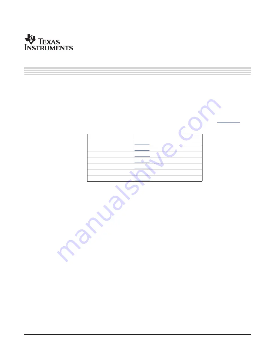
EVM-Compatible Device Data Sheets

Device

Literature Number

TLV320AIC34

SLAS538

TAS1020B

SLES025

REG1117-3.3

SBVS001

TPS767D318

SLVS209

SN74LVC125A

SCAS290

SN74LVC1G125

SCES223

SN74LVC1G07

SCES296

Contents

1

EVM Overview

...............................................................................................................

3

2

EVM Description and Basics

...............................................................................................

3

3

TLV320AIC34EVM-K Setup and Installation

.............................................................................

8

4

TLV320AIC34EVM Software

..............................................................................................

10

Appendix A

EVM Connector Descriptions

...................................................................................

36

Appendix B

TLV320AIC34EVM Schematic

..................................................................................

40

Appendix C

TLV320AIC34EVM Layout Views

..............................................................................

41

Appendix D

TLV320AIC34EVM Bill of Materials

............................................................................

44

Appendix E

USB-MODEVM Schematic

......................................................................................

45

Appendix F

USB-MODEVM Bill of Materials

................................................................................

46

Appendix G

USB-MODEVM Protocol

.........................................................................................

48

List of Figures

1

TLV320AIC34EVM-K Block Diagram

.....................................................................................

4

2

Default Software Screen

...................................................................................................

9

3

I

2

C Address Selection Window

..........................................................................................

10

4

Default Configuration Tab

.................................................................................................

12

5

Audio Input Tab

............................................................................................................

13

6

Audio Interface Tab

.......................................................................................................

15

7

Clocks Tab

.................................................................................................................

16

8

GPIO Tab

...................................................................................................................

18

9

AGC Tab

....................................................................................................................

20

10

Left AGC Settings

..........................................................................................................

21

I

2

S, I

2

C are trademarks of Koninklijke Philips Electronics N.V.

Windows is a trademark of Microsoft Corporation.
LabView is a trademark of National Instruments.
All other trademarks are the property of their respective owners.

SLAU232 – December 2007

TLV320AIC34EVM-K

1

Submit Documentation Feedback

Summary of Contents for TLV320AIC34EVM-K

Page 1: ...3 SBVS001 TPS767D318 SLVS209 SN74LVC125A SCAS290 SN74LVC1G125 SCES223 SN74LVC1G07 SCES296 Contents 1 EVM Overview 3 2 EVM Description and Basics 3 3 TLV320AIC34EVM K Setup and Installation 8 4 TLV320...

Page 2: ...C 1 Assembly layer 41 C 2 Top Layer 41 C 3 Layer 3 42 C 4 Layer 4 42 C 5 Bottom Layer 43 List of Tables 1 USB MODEVM SW2 Settings 5 2 List of Standalone Jumpers 5 3 List of Jumpers Connected to J17A D...

Page 3: ...TLV320AIC34EVM K is a complete evaluation demonstration kit which includes a USB based motherboard called the USB MODEVM Interface board and evaluation software for use with a personal computer runni...

Page 4: ...id bending the connecting pins The two boards can only be connected in one way It is suggested to first align with the 10 pin connectors J15B on the TLV320AIC34EVM and J18A on the USB MODEVM and then...

Page 5: ...Table 2 List of Standalone Jumpers Default Jumper Position Jumper Description JMP1 2 3 When connecting 2 3 mic bias comes from the MICBIAS pin on the device when connecting 1 2 mic bias is supplied f...

Page 6: ...in 9 Connects Block A WCLK_A and Block B WLCK_B together for ease of evaluation When Block A and Block B use different and digital clocks data this jumper MUST be removed WCLK_B DIN_A pin 10 pin Conne...

Page 7: ...k B analog outputs to the EVM can be connected through J13 and J14 top or bottom The connection details can be found in Table A 1 The digital inputs and outputs of the EVM can be monitored through J16...

Page 8: ...no further power supplies are necessary If lab supplies are used to provide the individual voltages required by the USB MODEVM Interface JMP6 should have no shunt installed Voltages are then applied t...

Page 9: ...ware and begin an initialization process The user may be prompted to identify the location of the drivers or allow the PC to automatically search for them Allow the automatic detection option 5 Once t...

Page 10: ...the settings of SW2 located on the EVM Table 2 When ADDR_A and ADDR_B are adjusted the correct device address for Block A and Block B will be shown Note that the actual I2 C address shown and the add...

Page 11: ...rack of register settings when toggling between Block A and Block B When using both Block A and Block B register updates it is recommended to either use I2 C scripts for both blocks or use GUI control...

Page 12: ...on is made the Preset Configuration Description are shows a summary of the codec setup associated with the choice made If the choice is acceptable the Load button can be pressed and the preset configu...

Page 13: ...ect to one ADC 3 Adjust the Level control to the desired attenuation for the connected channel This level adjustment can be done independently for each connection The TLV320AIC34 offers a programmable...

Page 14: ...ng for each channel is selected using the pull down menu control The two large knobs set the actual ADC PGA Gain and allow adjustment of the PGA gains from 0dB to 59 5dB in 0 5dB steps excluding Mute...

Page 15: ...n be soft muted when doing the re sync if the Soft Mute button is enabled In the upper right corner of this tab is the Digital Mic Functionality control The TLV320AIC34 can accept a data stream from a...

Page 16: ...allow operation from the USB MODEVM clock reference the EVM settings can be restored automatically by pushing the Load EVM Clock Settings button at the bottom of this tab Note that changing any of th...

Page 17: ...t reference frequency is entered into the PLLCLK_IN Source box in megaHertz MHz 2 The desired Fsref should be set using the Fsref switch 3 Push the Search for Ideal Settings button The software will s...

Page 18: ...t AGC Noise Threshold detection Jack Headset detection For use as an interrupt output the behavior of the interrupt can be selected using the Interrupt Duration control A Single 2ms pulse can be deliv...

Page 19: ...C so the SDA and SCL groupboxes and controls within them are disabled The MFP3 Function control selects MFP3 to be used either as a General Purpose Input or as the data input line for the alternate I2...

Page 20: ...The Left Right AGC Settings button determines the mode selection The Standardmode provides several preset times that can be selected by adjustments made to the Attackand Decayknobs If finer control o...

Page 21: ...ise gate functions such as Hysteresis Enable Clip stepping Threshold dB Signal Detect Debounce ms and Noise Detect Debounce ms are set using the corresponding controls in the Noise Gate groupbox for e...

Page 22: ...routed through the digital effects filtering before passing through the optional de emphasis filter before the DAC The digital effects filtering can only be connected to either the ADC or DAC not bot...

Page 23: ...the programmable function allows custom coefficients to achieve a different filter than provided by the preset filters The controls for the programmable high pass filter are located under the Program...

Page 24: ...nse will be shown on the Effect Filter Response graph however note that this response is not included in graphs of other effect responses when on the other filter design tabs Figure 16 De emphasis Fil...

Page 25: ...coefficients are not loaded into the TLV320AIC34 until the Download Coefficients button is pressed To avoid noise during the update of coefficients it is recommended that the user uncheck the Effect F...

Page 26: ...Biquads are quite good at simulating analog filter designs For each biquad section on this tab enter the desired analog filter type to simulate Butterworth Chebyshev Inverse Chebyshev Elliptic or Bes...

Page 27: ...on of one of four preset filter responses Rock Jazz Classical or Pop Figure 21 Preset Filters If filter coefficients are known they can be entered directly on this tab see Figure 22 for both biquads f...

Page 28: ...this effect properly make sure the appropriate coefficients are already loaded into the two biquad sections The User Filters tab may be used to load the coefficients See Figure 23 Figure 23 3D Effect...

Page 29: ...using the Common Mode Voltage control The TLV320AIC34 offers several options to help reduce the turn on off pop of the output amplifiers The Power On Delay of the output drivers can be set using the c...

Page 30: ...h offer debounce times in varying numbers of milliseconds See the TLV320AIC34 data sheet for a discussion of headset detection Output short circuit protection can be enabled in the Short Circuit Prote...

Page 31: ...t Volume knob setting Data going to the DACs is selected using the drop down boxes under the Left and Right DAC Datapath Each DAC channel can be selected to be off use left channel data use right chan...

Page 32: ...for the line output can also be controlled using the button below this master output knob Powered Up If the DAC Output Path control is set to Mix with Analog Inputs the six knobs in each panel can be...

Page 33: ...to the corresponding outputs or may be set to be a common mode voltage Constant VCM Out When used in these configurations the Powered Up button for the HPxCOM output is disabled as the power mode for...

Page 34: ...uted the return packets of data which result from each command will be displayed in the Read Data array control When executing several commands the Read Data control shows only the results of the last...

Page 35: ...20AIC34EVM software Figure 28 File Menu Under the Help menu is an About menu item which displays information about the TLV320AIC34EVM software The actual USB protocol used as well as instructions on w...

Page 36: ...C1 or LINE1 Analog Input Left Plus or Multifunctional J13 7 LINE1RM_B MIC1 or LINE1 Analog Input Right Minus or Multifunctional J13 8 LINE1RP_B MIC1 or LINE1 Analog Input Right Plus or Multifunctional...

Page 37: ...tors DESIGNATOR Description PIN 1 PIN 2 PIN3 J1 2 Connector Screw LINE1LP_A LINE1LM A NA Terminal Input J2 2 Connector Screw LINE1RP_A LINE1RM_A NA Terminal Input J3 2 Connector Screw LINE2LP_A LINE2L...

Page 38: ...ted J16 10 DGND Digital Ground J16 11 NC Not Connected J16 12 NC Not Connected J16 13 NC Not Connected J16 14 AIC34 RESET Reset J16 15 NC Not Connected J16 16 SCL I2 C Serial Clock J16 17 NC Not Conne...

Page 39: ...common power bus for the TLV320AIC34EVM Power is supplied on the pins listed in Table A 4 Table A 4 Power Supply Pin Out SIGNAL PIN NUMBER SIGNAL NC J15 1 J15 2 NC 5VA J15 3 J15 4 NC DGND J15 5 J15 6...

Page 40: ...m Appendix B TLV320AIC34EVM Schematic Appendix B The schematic diagram for the modular TLV320AIC34EVM is provided as a reference 40 TLV320AIC34EVM Schematic SLAU232 December 2007 Submit Documentation...

Page 41: ...COM_B HPRCOM_B MICBIAS_B MICDET_B LINE1LP_B LINE1RP_B LINE1LM_B LINE1RM_B MONO_LOP_B MONO_LOM_B LINE2LP_B LINE2RP_B LEFT_LOP_B RIGHT_LOP_B LINE2LM_B LINE2RM_B LEFT_LOM_B RIGHT_LOM_B MCLK_B BCLK_B WCLK...

Page 42: ...AGND 17 AGND 19 J14 DAUGHTER ANALOG MCLK_A BCLK_A WCLK_A DIN_A DOUT_A RESET_A GPIO1_A GPIO2_A SDA SCL TP40 AGND TP41 DGND J13A TOP SAM_TSM 110 01 L DV P J13B BOTTOM SAM_SSW 110 22 F D VS K J16A TOP S...

Page 43: ...US MINUS 1 2 J3 LINE 2 LEFT IN_A 1 2 J4 LINE 2 RIGHT IN_A PLUS MINUS PLUS MINUS TP1 LINE1LP_A TP2 LINE1LM_A TP3 LINE1RP_A TP4 LINE1RM_A TP5 LINE2LP_A TP6 LINE2LM_A TP7 LINE2RP_A TP8 LINE2RM_A GPIO2_A...

Page 44: ...GPIO1_B C47 0 1uF TP52 MIC3L_B C44 NI TP51 MICDET_B 1 2 JMP20 HPCOM_B HPLOUT_B HPROUT_B HPLCOM_B HPRCOM_B C43 C44 and C45 are not installed but can be used to filter noise C35 0 1uF C36 0 1uF C37 0 1u...

Page 45: ...www ti com Appendix C TLV320AIC34EVM Layout Views Appendix C Figure C 1 Assembly layer Figure C 2 Top Layer SLAU232 December 2007 TLV320AIC34EVM Layout Views 41 Submit Documentation Feedback...

Page 46: ...www ti com...

Reviews: