background image

www.ti.com

AIC3212 Control Software

3.2

Using the AIC3212EVM-U CS

The following sections describe the AIC3212EVM-U CS usage.

3.2.1

Main Panel Window

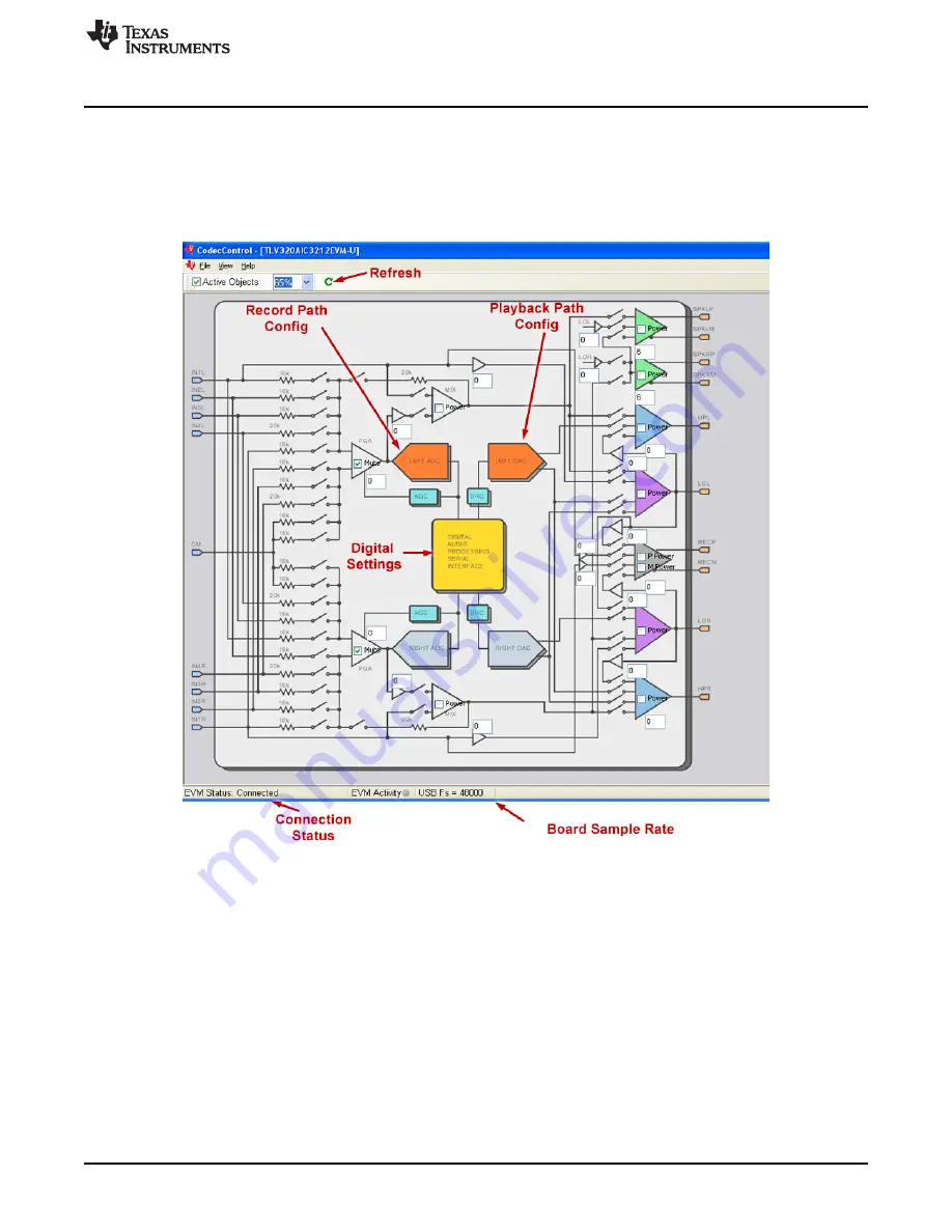
The Main Panel window, shown in

Figure 4

, provides easy access to all the features of the AIC3212 CS.

Figure 4. Main Panel Window

The main panel provides a high-level block diagram of the AIC3212. On the main panel, shown in

Figure 4

, users can configure the analog input and output routings by simply clicking on the switches. The

analog setup, digital setup, audio inputs, audio outputs, DRC, AGC, SAR and headset detection provide
additional control of many other features of the AIC3212. These categories are intended for advanced
users and can be accessed by clicking “View” on the main panel. One can also click on the colored blocks
on the main panel to gain access to these categories. Left ADC and Right ADC blocks provide detailed
settings for recording path. Left DAC and Right DAC blocks provide detailed settings for playback path.
Yellow block in the middle provides settings for digital interface, which includes Audio Serial Interface
configuration, clock settings, etc.

Clicking “Refresh” button on the top will read back the current state of the AIC3212 register settings and
reflect it to the user interface. “EVM status” on the bottom part of the main panel reflects the hardware
connection of the EVM. “USB Fs” indicates the current sample rate of the EVM board.

7

SLAU435 – March 2012

TLV320AIC3212EVM-U Evaluation Module

Submit Documentation Feedback

Copyright © 2012, Texas Instruments Incorporated

Summary of Contents for TLV320AIC3212EVM-U

Page 1: ...ts 32 9 1 Headphone playback script 32 9 2 Microphone recording script 33 10 Related Documentation 35 List of Figures 1 Top view of TLV320AIC3212EVM U board 2 2 USB Connection 4 3 Using Example Config...

Page 2: ...ion to the PC provides power control and streaming audio for quick and easy evaluation Easy to use AIC3212 Control Software CS provides a graphical user interface to configure and control the TLV320AI...

Page 3: ...ip and the ring J3 SPEAKER SPKLP SPKLM Stereo Class D Speaker Outputs OUTPUTS SPKRP SPKRM J4 HP OUT HPL HPR Headphone Output J5 REC OUT RECP RECM Receiver Output J6 SAR REF VREF_SAR External voltage s...

Page 4: ...ct folder The password for installation is CC 3 Connect the TLV320AIC3212EVM to an available USB port LED lights D1 and D2 should illuminate once the EVM is detected by PC Also in the Windows device m...

Page 5: ...Software and select a typical headphone playback script as shown in Figure 3 Figure 3 Using Example Configurations in Control Software 5 SLAU435 March 2012 TLV320AIC3212EVM U Evaluation Module Submit...

Page 6: ...eration and installation of the AIC3212 control software 3 1 AIC3212EVM CS Setup To install the TLV320AIC3212 EVM U software 1 Download the latest version of the AIC3212EVM U Control Software CS locat...

Page 7: ...d users and can be accessed by clicking View on the main panel One can also click on the colored blocks on the main panel to gain access to these categories Left ADC and Right ADC blocks provide detai...

Page 8: ...cal record and playback configurations can be accessed by choosing Example Configuration under View Once the typical configuration is selected click ProgramCodec to download the script into EVM Figure...

Page 9: ...the codec A script is loaded into the command buffer either by loading a script file using the open button or by pasting text from the clipboard Click Run to execute the command buffer All controls u...

Page 10: ...ecode Window Another feature in the command line interface is the Record function By checking the Record box one can record the current value of the register that is being modified The recorded regist...

Page 11: ...ains information such as register name current register value and the bit field of the current register value While using the register inspect table user should first specify the page number Once the...

Page 12: ...ns of the PCB as shown below are 165mm 91 4mm 6 5 3 6 inches Figure 9 TLV320AIC3212EVM PCB Top Figure 10 TLV320AIC3212EVM PCB Layer 2 12 TLV320AIC3212EVM U Evaluation Module SLAU435 March 2012 Submit...

Page 13: ...Figure 11 TLV320AIC3212EVM PCB Layer 3 Figure 12 TLV320AIC3212EVM PCB Bottom Copper Reversed 13 SLAU435 March 2012 TLV320AIC3212EVM U Evaluation Module Submit Documentation Feedback Copyright 2012 Te...

Page 14: ...i com Figure 13 TLV320AIC3212EVM PCB Bottom Figure 14 TLV320AIC3212EVM PCB Drill Pattern 14 TLV320AIC3212EVM U Evaluation Module SLAU435 March 2012 Submit Documentation Feedback Copyright 2012 Texas I...

Page 15: ...2 DOUT2 DIN3 GPI2 GPO1 CPFCP LOR CPVDD_18 AVDD4_18 DVSS SPI_SELECT GPI4 DOUT3 BCLK3 SLVDD AVSS4 SPKLM SRVSS SPK_V GPIO2 IOVSS GPIO1 RESET SPKLP SLVSS SPKRM SRVDD SPKRP MCLK2 VBAT IOVDD DVDD DVDD IOVDD...

Page 16: ...F C16 0 1uF C15 0 1uF C14 IOVD IOVD SCL_IOVD SDA_IOVD GND GND SN74LVC1G126DBVR U7 3 5 4 2 1 0 1uF C18 IOVD GND GND 1 2 4 5 3 U6 SN74LVC1G126DBVR 0 1uF C17 IOVD GND 200K R14 PCA9306DCTR U4 8 7 6 5 4 3...

Page 17: ...J3 F4 H9 J4 GND GND GND GND C95 0 1uF 5V VR1 TPS73633DBVT 5 4 3 2 1 C98 47uF C97 10uF C96 0 1uF C36 2 2uF 3 3VD W14 3 2 1 5V R17 221 C49 0 1uF GND TP57 3 3VD C48 10uF JP2 1 2 3 JP3 3 2 1 1 2 J11 GND R...

Page 18: ...60 0 0047uF C99 0 0047uF C102 0 0047uF C100 GND GND GND GND FLT_RP FLT_RM FLT_LM FLT_LP 16 R63 GND J19 5 6 3 1 4 2 Shield RIGHT LEFT GND 16 R62 GND 2 1 W18 2 1 W47 GND 221 R68 0 1uF C107 10uF C106 1 2...

Page 19: ...2 1 W51 3 2 1 W52 3 2 1 GND IOVD W53 1 2 3 W54 1 2 3 GND IOVD W50 1 2 3 DIN SDOUT1 BCLK WCLK DOUT1 DIN1 SRC2_MCLK DOUT2 DIN2 DOUT3 DIN3 GPO1_DOUT GPI2_DIN DOUT3 SRC1_MCLK W58 1 2 W59 1 2 MCLK2 MCLK1...

Page 20: ...A SN74LVC1G07DBVR 1 2 3 4 5 U18 NC GND Y VCC A SN74LVC1G07DBVR 1 2 3 4 5 U19 NC GND Y VCC A SN74LVC1G07DBVR 1 2 3 4 5 U20 NC GND Y VCC A IOVD GND R70 4 75K R69 357 LOCK_SRC2 Green 3 3VD R72 4 75K R71...

Page 21: ...8 7 6 5 4 3 2 1 13 C91 0 1uF TORX147PL F T TORX147PL F T J17 3 2 1 OUT Vcc GND SHIELD C86 0 1uF C87 0 1uF C90 0 1uF R50 4 7K R45 10 C85 10uF R46 10 C88 10uF GND GND GND GND GND GND GND 1 8V GND GND C...

Page 22: ...5in HW8 3 3VD 3 3VD DOUT1 DIN1 DOUT2 DIN2 DOUT3 DIN3 GPO1_DOUT GPI2_DIN MICDET MICBIAS MCLK2 MCLK1 MCLK1 DGND I2S_ENABLE DGND I2S1 DGND MCLK I2C RESERVED RESERVED DV_ENABLE VARVD VARVD 1 8VD 1 8VD 3...

Page 23: ...9 1 U11 DUAL POS EDGE TRIG D TYPE FLIP FLOP W CLR PRE DIGI KEY 296 1241 1 ND TEXAS INSTRUMENTS SN74LVC74APWR TSSOP8 PW ROHS 10 4 U1 U18 U19 U20 SINGLE BUFFER DRIVER GATE OPEN DRAIN OUTS DIGI KEY 296...

Page 24: ...27 4 C19 C22 C25 C97 CAP SMD0603 CERM 10UFD 10V 20 X5R ROHS DIGI KEY PCC2479CT PANASONIC ECJ 1VB1A106M 28 2 C35 C36 CAP SMD0603 CERM 2 2UFD 10V 10 X7R ROHS DIGI KEY 490 4520 1 MURATA GRM188R71A225KE15...

Page 25: ...6 10 0 OHM 1 1 4W ROHS DIGI KEY P10 0FCT PANASONIC ERJ 8ENF10R0 R51 50 1 R14 RESISTOR SMD0603 200K OHMS 5 1 10W ROHS DIGI KEY P200KGCT PANASONIC ERJ 3GEYJ204V 51 4 R29 R30 R77 R78 RESISTOR SMD0603 0 0...

Page 26: ...RU MALE 2X3 PIN 100LS GOLD ROHS DIGI KEY S2011E 03 SULLINS PBC03DAAN 65 2 P1 P2 PLUG SMD 2x50 FEMALE JMDSERIES 0 5MM LS GOLD DIGI KEY 455 1880 1 JST 100P JMDSS G 1 ROHS TF LF SN 66 4 J2 J4 J5 J19 JACK...

Page 27: ...2 DGND3 SGND1 ELECTRONICS SGND2 72 6 1 8V 1 8V_CP 3 3V PC TESTPOINT RED ROHS DIGI KEY 5000K KEYSTONE 5000 3 3VD 5V VARVD ELECTRONICS 73 4 SW1 SW2 SW3 SW4 SWITCH MOM 160G SMT 4X3MM ROHS DIGI KEY EG4344...

Page 28: ...W24 1 2 Selection for External MCLK2 W25 2 3 Configuration for Audio Serial Interface 1 DIN1 W26 2 3 Configuration for Audio Serial Interface 1 BCLK1 W27 2 3 Configuration for Audio Serial Interface...

Page 29: ...ion for GPI3 W53 2 3 6 wire I2S enable on GPI4 W54 1 2 Pull up or Pull down Selection for GPI4 W55 1 2 Load Selection for Headphone HPL Output W56 1 2 Load Selection for Headphone HPR Output W57 1 2 S...

Page 30: ...times This feature is useful when switching buffers in parts that support the adaptive filtering mode The command f syntax follows f i2c address register D7 D6 D5 D4 D3 D2 D1 D0 where i2c address and...

Page 31: ...06b The following example demonstrates usage of the Wait for Flag command f example script for wait for flag command I i2cfast Switch to Page 44 w 30 00 2C Switch buffer w 30 01 05 Wait for bit D0 to...

Page 32: ...elect MCLK for CODEC clock input bypass PLL w 30 04 00 NDAC 1 MDAC 2 w 30 0B 81 w 30 0C 82 DOSR 128 w 30 0D 00 w 30 0E 80 Initialize the Codec select page 1 w 30 00 01 Disable weak connection between...

Page 33: ...one power up in Ground centered Mode w 30 23 10 Enable DAC to HPL HPR and power up HPL HPR w 30 1B 33 select page 0 w 30 00 00 power up DAC_L and DAC_R w 30 3F C0 Unmute the DAC digital volume control...

Page 34: ...onnection beween AVDD and DVDD w 30 01 00 set the REF charging time to 40 ms w 30 7A 01 Set the quick charge of input coupling cap for analog inputs w 30 79 33 ASI 1 configuration select page 4 w 30 0...

Page 35: ...dance w 30 37 20 w 30 39 80 Left Channel Analog ADC PGA 30 dB w 30 3B 3C Right Channel Analog ADC PGA 30 dB w 30 3C 3C ADC Analog programmed for PTM_R4 w 30 3D 00 select page 0 w 30 00 00 Power up ADC...

Page 36: ...o handling the product This notice contains important safety information about temperatures and voltages For additional information on TI s environmental and or safety programs please contact the TI a...

Page 37: ...or use in safety critical applications such as life support where a failure of the TI product would reasonably be expected to cause severe personal injury or death unless officers of the parties have...

Reviews: