


TNETX3270
ThunderSWITCH
24/3 ETHERNET
SWITCH
WITH 24 10-MBIT/S PORTS AND 3 10-/100-MBIT/S PORTS
SPWS043B – NOVEMBER 1997 – REVISED APRIL 1999
1
POST OFFICE BOX 655303
•
DALLAS, TEXAS 75265
D
Port Configurations:
Twenty-Four 10-Mbit/s Ports
– Ports Arranged in Three Groups of Eight
Ports in a Multiplexed Interface
– Direct Multiplexer Interface to
TNETE2008
– Full and Half Duplex
– Half-Duplex Collision-Based Flow
Control
– Full-Duplex IEEE Std 802.3x Flow Control
– Interoperable Support for IEEE
Std 802.1Q VLAN
– Speed, Duplex, and Pause
Autonegotiation With Physical Layer
(PHY)
Three 10-/100-Mbit/s Ports
– Direct Interface to TNETE2101
– Full and Half Duplex
– Half-Duplex Collision-Based Flow
Control
– Full-Duplex IEEE Std 802.3x Flow Control
– Interoperable Support for IEEE
Std 802.1Q VLAN
– Pretagging Support
D
Port Trunking and Load Sharing
D
LED Indication of Port Status
D
SDRAM Interface
– Direct Interface to 8-Bit/Word and
16-Bit/Word, 16-Mbit, and 64-Mbit
SDRAMs
– 32-Bit-Wide Data Bus
– Up to 32 Mbytes Supported
– 83.33-MHz SDRAM Clock
– 12-ns (–12) SDRAMs Required
D
Remote Monitoring (RMON) Support –
Groups 1, 2, 3, and 9
D
Direct I/O (DIO) Management Interface
– Eight Bits Wide
– CPU Access to Statistics, Registers, and
Management Information Bases (MIBs)
– Internal Network Management Port
– Forwards Spanning-Tree Packets to CPU
– Serial Media-Independent Interface (MII)
for PHY Control
D
EEPROM Interface for Autoconfiguration
(No CPU Required for Nonmanaged Switch)
D
Internal Address-Lookup/Frame-Routing
Engine
– Interoperable Support for IEEE
Std 802.1Q VLAN
– Supports IEEE Std 802.1D Spanning Tree
– Thirty-Two Assignable Virtual LANs
(VLANs)
– Multiple Forwarding Modes
– 2K Total Addresses Supported
– Port Mirroring
D
IEEE Std 1149.1 (JTAG) Interface (3.3-V
Signals)
D
2.5-V Process With 3.3-V-Drive I/O
D
Packaged in 240-Terminal Plastic Quad
Flatpack
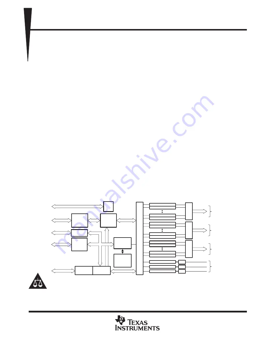
Eight Ports
(16–23)
10 Mbit/s
Controller (MAC)
Controller (MAC)
Controller (MAC)
TAP
(JTAG)
Address
Compare
Statistics
Storage
MIB
Three Ports
(24–26)
10/100 Mbit/s
Network
Statistics
Logic
Data Path
LED
Interface
CPU
Interface
SDRAM
Controller
Controller (MAC)
Controller (MAC)
Controller (MAC)
Controller (MAC)
MUX
Controller (MAC)
Controller (MAC)
MII
MII
MII
Eight Ports
(08–15)
10 Mbit/s
Eight Ports
(00–07)
10 Mbit/s
Queue
Manager
EEPROM
Interface
Controller (MAC)
Controller (MAC)
Controller (MAC)
Controller (MAC)
MUX
Controller (MAC)
Controller (MAC)
MUX
Copyright
1999, Texas Instruments Incorporated
PRODUCTION DATA information is current as of publication date.
Products conform to specifications per the terms of Texas Instruments
standard warranty. Production processing does not necessarily include
testing of all parameters.
Please be aware that an important notice concerning availability, standard warranty, and use in critical applications of
Texas Instruments semiconductor products and disclaimers thereto appears at the end of this data sheet.
TI and ThunderSWITCH are trademarks of Texas Instruments Incorporated.
Ethernet is a trademark of Xerox Corporation.
Secure Fast Switching is a trademark of Cabletron Systems, Inc.
Port-trunking and load-sharing algorithms were contributed by Cabletron Systems, Inc. and are derived from, and compatible with, Secure Fast
Switching
.


