


TAS54x4C Hardware Design Guidelines
During the turn-on of the amplifier, the input coupling capacitors must charge to the common mode
voltage of 3.25 VDC. If the amplifier is passing a signal during this time, the speakers can have large
excursions, pops, and click. The TAS54x4C devices have a precharge resistor on the inputs to quickly
charge the coupling capacitors. After the capacitor is charged, the resistor is taken out of the circuit and
the 80 k
Ω
resistor is in place. This worst-case value of the precharge resistor is 600
Ω
.
calculates the charge time using the worse case value from the example in
of 1.2 µF and 600
Ω
.
V
I(x)
= V
I(x)
max × (1 – e
–t / RC
)
(2)
The input capacitors should have good audio qualities as the audio input signal to the amplifier passes
directly through it. A good-quality capacitor can be a film type or a very-low leakage electrolytic. Ceramic
capacitors can be used, but can degrade the sound quality. Low leakage on the capacitor is important for
low direct-current (DC) offset at the output of the amplifier. The TAS54x4C amplifiers provide gain at DC.
Any leakage current will flow through the 80-k
Ω
input impedance and cause a small DC offset between
the input pins. This small DC offset will be amplified by the gain setting.
1.2
I
2
C Communication
Three pins are associated with the I
2
C communication protocol. Both devices have the clock pin (SCL)
and the data pin (SDA), while the address selection pin is labeled I2C_ADDR on the TAS54x4C devices.
1.2.1
Device Address Selection
The TAS54x4C devices have the capability of using four different I
2
C addresses. The devices in this family
share the same I
2
C device addresses which allows for up to four TAS5414C and TAS5424C devices to be
controlled by one I
2
C controller without I
2
C bus switches. The I
2
C address is determined by the DC voltage
present on the address selection pin. The I
2
C-address pin voltage is sensed when the device is released
from standby mode. This voltage is then latched at 300 µs. Therefore, any noise or voltage glitch cannot
change the I
2
C address during operation. Because this pin latches when released from standby, a
capacitor is not necessary on this pin. The charge time on the capacitor may cause an incorrect I
2
C
address.
NOTE:
Do not confuse the master-slave notation with a master-slave I
2
C.
A slave device must have an external oscillator connected to the OSC_SYNC pin (see
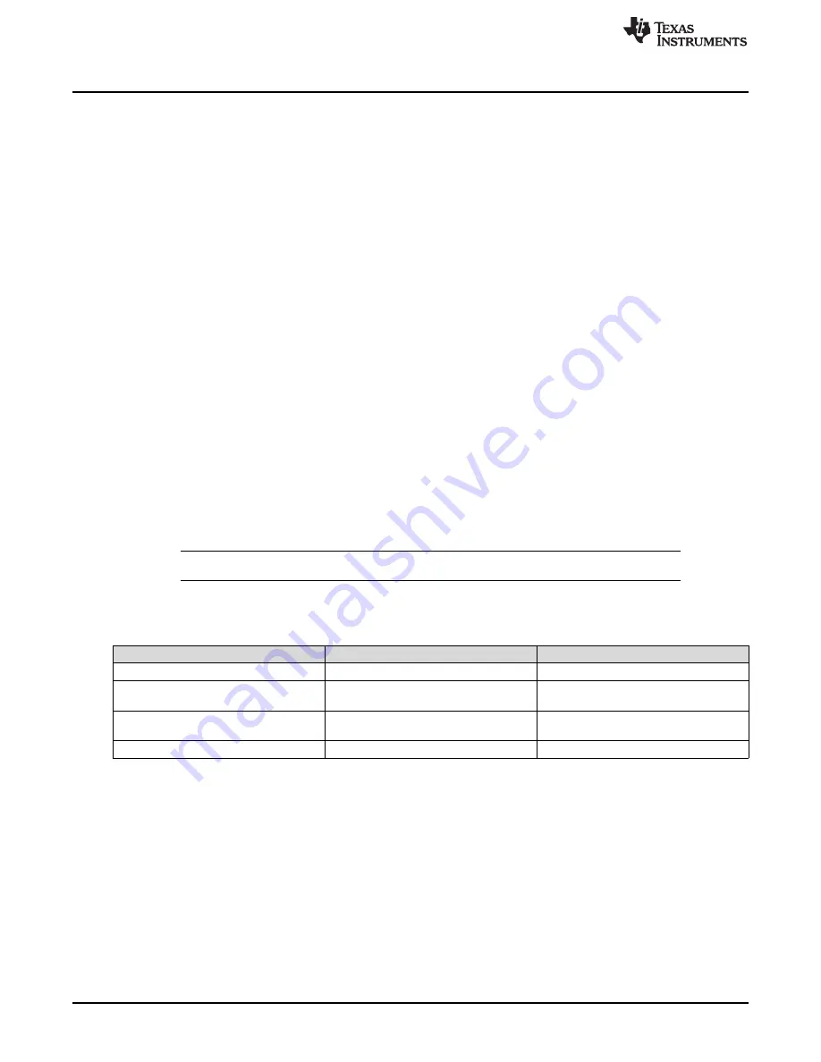
Table 1. Oscillator Configuration and I
2
C Addresses
OSCILLATOR CONFIGURATION
I2C_ADDR PIN CONNECTION
I
2
C ADDRESS
Master
To SGND Pin
0xD8, 0xD9
Slave 1
35% DVDD (resistive voltage divider
0xDA, 0xDB
through D_BYP Pin and SGND Pin)
Slave 2
65% DVDD (resistive voltage divider
0xDC, 0xDD
through D_BYP Pin and SGND Pin)
Slave 3
To D_BYP Pin
0xDE, 0xDF
1.2.2
I
2
C Communications
The SDA and SCL pins communicate with an I
2
C controller. The SDA pin carries the data and the SCL pin
carries the clock. The TAS54x4C devices are I
2
C slave-only devices. The device cannot start I
2
C
transactions and cannot generate an I
2
C clock. The SCL pin is set for input signals only, whereas the SDA
pin is bidirectional. The TAS54x4C devices send data when the I
2
C controller sends a read command. The
SDA and SCL pins require pullup resistors to 3.3 VDC or 5 VDC because these pins are 5 VDC tolerant.
A resistor value of 4.7 k
Ω
can be used for proper operation. The resistor value should be adjusted to the
number of devices on the I
2
C bus according to the I
2
C specification.
The TAS5414C and TAS5424C devices have the capability to receive and send sequential data. All
registers can be read sequentially except the fault registers. All registers with write capabilities can be
written sequentially.
4
TAS54x4C Design Guide
SLOA196 – June 2014
Copyright © 2014, Texas Instruments Incorporated


