


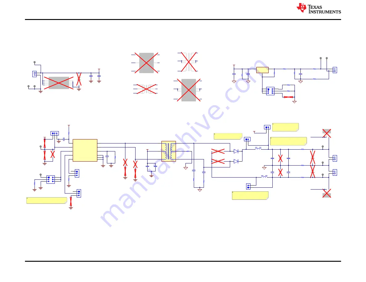
6 EVM Schematic and PCB
shows the schematic diagram for this EVM, and
show the printed circuit board (PCB) layout.
GND
GND
R11
R10
C11
C12
GND
GND
ISO_GND
GND
2
1
D1
PMEG200G20ELRX
TP7
+VOUT
TP8
GND_OUT
TP9
-VOUT
TP4
GND
1
2
3
J5
1
2
3
J14
EN_High
EN_Low
EXT_CLK
CLK_adjust. (RCLK)
GND
ISO_GND
2
1
D5
PMEG200G20ELRX
2
1
D4
PMEG200G20ELRX
2
1
D2
PMEG200G20ELRX
VCC
3
SW1
1
SW2
10
CLK
7
DC
5
EN/UVLO
4
SR
6
SS/ILIM
8
GND
2
GND
9
EP
11
SN6507DGQ
U2
TP1
VIN
TP5
GND
EN/UVLO_IN
CLK_GND (default)
GND
GND
18.2k
Rilim
GND
1
2
J8
1
2
J11
50.5k
Rdc
10V
2.2uF
Css
Vout = 1.25V x (1+R5/R4) + (50uA x R5)
1
2
J2
1751248
GND
GND
VIN
Input Power
SN6507 Vcc range 3V-36V
10uF
C3
1µF
C4
IN
3
OUT
4
1
ADJ
LM317AMDT/NOPB
U1
1
2
J1
1751248
Output Power
10k
R3
240
R4
0
R1
VIN
100nF
C5
10uF
C13
VIN
VLDO in 4.25V-40V
1
2
3
J6
1
2
3
4
5
6
J10
TSM-103-01-L-DV
1
2
J4
+VOUT_LDO_IN
10uF
C8
10uF
C17
1uF
C9
1uF
C18
1
2
3
J13
DC_48% (default)
DC Control
GND
GND
ISO_GND
TP2
+VOUT_LDO
TP3
GND_OUT
15V R option
12V R option
R5 = (Vout-1.25) / ([1.25/R4]+50uA)
DNP R option
2.61k
R5A
2.05k
R5B
0
R5C
1
2
3
4
5
6
J3
TSM-103-01-L-DV
ISO_GND
TP10
CLK_IN
TP6
EN_IN
499k
Ruv1
100k
Ruv2
10uF
C7
ISO_GND
10uF
C2
10k
R2
0
R9
20.5k
Rsr
1
2
3
J9
Default SR
SR adjust.
SR Control
L1
L2
100nF
C14
100nF
C1
100nF
C10
100nF
C19
1
2
3
6
5
4
T1
750319696
36V
D3
36V
D6
1
2
3
4
5
6
7
8
ZB1459-BE
1
2
J7
1
2
J12
ISO_GND
XP5
XP6
XP4
XP3
XP2
XP1
VIN
XP1
XP2
XP3
XP4
XP5
XP6
XP1
XP2
XP3
XP6
XP5
XP4
1
2
3
6
5
4
PAG6356.086NLT
Extra Transformer Footprints
SN6507 Circuit
36V
D7
1
2
4
8
7
5
3
6
SM91207L
XP1
XP2
XP3
XP6
XP5
XP4
6
4
3
1
2
5
B1807127
IN
4
IN
5
GND
1
GND
2
IN
6
GND
3
PAD
7
TVS3300DRVR
U3
XP1
XP2
XP3
XP6
XP5
XP4
GND
0
Rclk
DC adjust.
0
R6
0
R7
0
R8
100nF
C6
+VOUT
GND_OUT
-VOUT
GND_OUT
GND_OUT
0
R15
GND_OUT
0
R14
ISO_GND
GND
0
R16
+VOUT_LDO_IN
62pF
C15
62pF
C16
100
R13
100
R12
Rclk, Rsr, Rdc, Rilim, Css can be adjusted per
SN6507 datasheet
Populate D1 and D4 for -Viso
output
J4 jumper:
populated = +Vout LDO ON
DNP = LDO bypassed
J7 jumper:
populated = L1 bypassed no DC CTRL
DNP = L1 for DC CTRL
J12 jumper:
populated = L1 bypassed no DC CTRL
DNP = L1 for DC CTRL
Figure 6-1. SN6507DGQEVM Schematic
Bill of Materials
10
SN6507DGQEVM Low-Emissions 500 mA Push-Pull Transformer Driver for Isolated Power Supplies
Evaluation Module
Copyright © 2022 Texas Instruments Incorporated