background image

External Component Selection

2-18

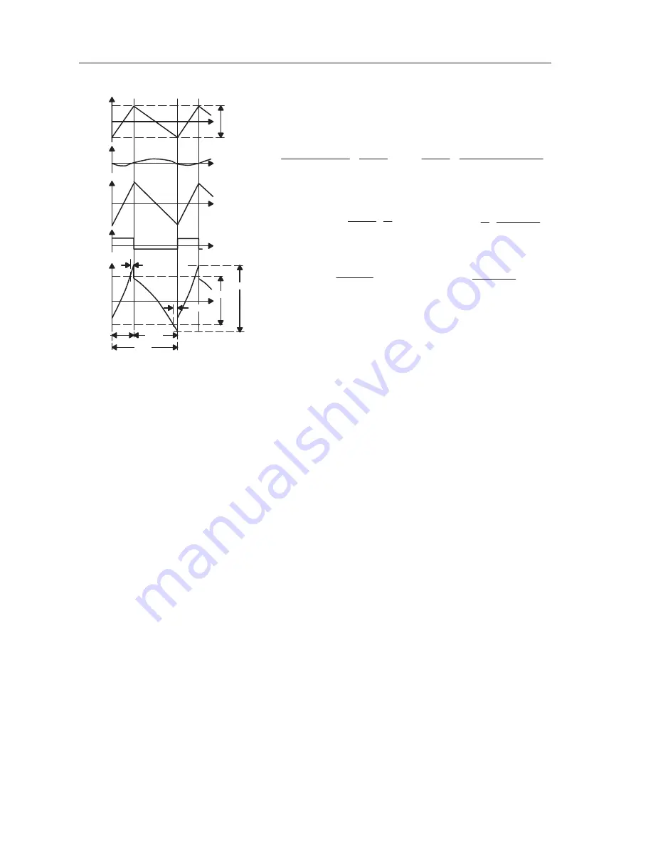
Figure 2–6. Output Ripple Voltage Detail

(a)

Current waveform through output capacitor

(b)

Voltage waveform across ideal capacitor with initial value at
beginning of high-side MOSFET on-time

V

C

+

I


t2

2


Co


D


Ts

I


t

2


Co

High-side MOSFET ON

High-side MOSFET OFF

V

C

+

I


t

2


Co

I


t2

2


Co


(1–D)


Ts

(c)

Voltage waveform across ESR

V

ESR

+

ESR


I


t

D


Ts

I

2

High-side MOSFET ON

High-side MOSFET OFF

V

ESR

+

ESR


I

2

I


t

(1

–D)


Ts

(d)

Voltage waveform across ESL

V

ESL

+

ESL


I

D


Ts

High-side MOSFET ON

High-side MOSFET OFF

V

ESL

+

ESL


I

(1

–D)


Ts

Hyst

(a)

(b)

(c)

(d)

(e)

IAC

∆Ι

VC

VESR

VESL

Vripple

tdel

t

t

t

t

tdel t

Vp–p

ton

toff

Ts

(e)

Composite output voltage ripple waveform

V

ripple

+

V

C

)

V

ESR

)

V

ESL

Figures 3–6, 3–15, 3–24, and 3–33 show the phase voltage (voltage at
junction of high-side MOSFET with low-side MOSFET), and output voltage
ripple waveforms for the example circuit of Figure 1–3. The output voltage
waveform is slightly different from the theoretical waveform of Figure 2–6(e)
due to the smoothing effect of the 10-

µ

F ceramic capacitor in parallel with the

electrolytic capacitors.

2.2.4.2

Switching Frequency Equation

Assume that the input and output voltage ripple magnitudes are relatively
negligible compared to the dc component. Also assume that the time constant
L/(R

DS(on)

 + R

L

), where L is the output inductance, R

L

 is the inductor resistance

and R

DS(on)

 is the on-state resistance of the high-side MOSFET(s), is high in

comparison with the switching period. Assume the body diode conduction time
and switching transition time are much smaller than the switching period.
These assumptions are reasonable for low voltage ripple and high efficiency
regulators. In such a case the output inductor current can be modeled as
the sum of the dc component, which is equal to the output current 

Io, and

the ac linear ramp component, which flows through the output capacitor
[Figure 2–6(a)].

The numbered equations in this section are used to derive the switching
frequency equation.

Summary of Contents for SLVU013

Page 1: ... June 1999 Mixed Signal Linear Products User s Guide SLVU013 ...

Page 2: ...CONDUCTOR PRODUCTS MAY INVOLVE POTENTIAL RISKS OF DEATH PERSONAL INJURY OR SEVERE PROPERTY OR ENVIRONMENTAL DAMAGE CRITICAL APPLICATIONS TI SEMICONDUCTOR PRODUCTS ARE NOT DESIGNED AUTHORIZED OR WARRANTED TO BE SUITABLE FOR USE IN LIFE SUPPORT DEVICES OR SYSTEMS OR OTHER CRITICAL APPLICATIONS INCLUSION OF TI PRODUCTS IN SUCH APPLICATIONS IS UNDERSTOOD TO BE FULLY AT THE CUSTOMER S RISK In order to ...

Page 3: ...hapter 1 Introduction Chapter 2 Design Procedure Chapter 3 Test Results Information About Cautions and Warnings This book may contain cautions and warnings This is an example of a caution statement A caution statement describes a situation that could potentially damage your software or equipment This is an example of a warning statement A warning statement describes a situation that could potentia...

Page 4: ...quipment is intended for use in a laboratory test environment only It gen erates uses and can radiate radio frequency energy and has not been tested for compliance with the limits of computing devices pursuant to subpart J of part 15 of FCC rules which are designed to provide reasonable protection against radio frequency interference Operation of this equipment in other en vironments may cause int...

Page 5: ...sion 2 7 2 1 6 Overcurrent Protection 2 7 2 1 7 Overvoltage Protection 2 10 2 1 8 Power Good 2 10 2 1 9 Bias 2 10 2 1 10 Gate Drivers 2 10 2 2 External Component Selection 2 14 2 2 1 Duty Cycle Estimate 2 14 2 2 2 Input Capacitance 2 14 2 2 3 Output Filter Design 2 14 2 2 4 Switching Frequency Analysis 2 17 2 2 5 Power MOSFET Selection 2 20 3 Test Results 3 1 3 1 Test Summary 3 2 3 1 1 Static Line...

Page 6: ...asured Switching Waveforms 3 9 3 7 SLVP111Measured Start Up INHIBIT Waveforms 3 9 3 8 SLVP111 Measured Start Up VCC Waveforms 3 10 3 9 SLVP111Measured Start Up VIN Waveforms 3 10 3 10 SLVP111 Measured Load Transient Waveforms 3 11 3 11 SLVP112 Measured Load Regulation 3 11 3 12 SLVP112 Measured Efficiency 3 12 3 13 SLVP112 Measured Power Dissipation 3 12 3 14 SLVP112 Measured Switching Frequency 3...

Page 7: ...er Dissipation 3 21 3 32 SLVP114 Measured Switching Frequency 3 22 3 33 SLVP114 Measured Switching Waveforms 3 22 3 34 SLVP114 Measured Start Up INHIBIT Waveforms 3 23 3 35 SLVP114 Measured Start Up VCC Waveforms 3 23 3 36 SLVP114 Measured Start Up VIN Waveforms 3 24 3 37 SLVP114 Measured Load Transient Waveforms 3 24 Tables 1 1 Summary of EVM Converter Modules 1 4 1 2 EVM Converter Operating Spec...

Page 8: ...viii ...

Page 9: ... are available for the converter and where isolation is not a requirement This user s guide describes techniques for designing synchronous buck converters using TI s SLVP111 114 EVMs and TPS56xx ripple regulator controllers Synchronous buck converters provide an elegant power supply solution for rapidly transitioning DSP loads such as the Texas Instruments TMS320C62x 67x family fast memory and sim...

Page 10: ... that its ON voltage drop is less than the forward drop of the original freewheeling rectifier thus increasing conversion efficiency A very important design issue when using a synchronous buck converter is preventing cross conduction of the two power MOSFETs i e preventing both MOSFETs from being on simultaneously A small amount of deadtime is necessary Figure 1 shows a simplified schematic of a s...

Page 11: ...plus one half of the hysteresis band VHi 2 525 V the TPS5625 turns off the high side MOSFET and turns on the low side MOSFET This is the power stage off state and it causes the output voltage to decrease This hysteretic method of control keeps the output voltage within the hysteresis band around the reference voltage If output load current steps or input voltage transients force the output voltage...

Page 12: ... selection criteria for powering circuit cards with multiple DSPs and for providing the regulated voltage to other hardware on the circuit card Component size can be reduced for designs requiring lower power levels The TPS56xx controllers each provide one of four popular output voltage levels The last two digits of the part number correlate to the set point voltage level TPS5633 is the 3 3 V contr...

Page 13: ... Vdc input voltage is not sufficient for proper operation Overload protection protects the power supply from accidental overloads or short circuits Overvoltage protection prevents damage to the load in the event of an internal power supply failure or presence of high voltages on the output from an external condition Both overvoltage and overcurrent cause a latched shutdown Both power MOSFETs are d...

Page 14: ...2 2 5 V SLVP113 1 8 V SLVP114 1 5 V 90 86 4 83 2 79 8 Efficiency 4 A load SLVP111 3 3 V SLVP112 2 5 V SLVP113 1 8 V SLVP114 1 5 V 91 6 88 6 85 1 81 9 Vi 5 V Io 6 A Io 6 A Vi 5 V 10 Vi 5 V Vi 5 V Io stepped repetitively from 0 A to 6 5 A Output current rating is limited by thermal considerations Load currents above this rating may cause damage to the power supply Unless otherwise specified all test...

Page 15: ...See Note C5 0 1 µ F R2 10 kΩ R1 1 kΩ C1 33 µ F 10 V L1 2 2 µ H C2 150 µ F 6 3 V C3 150 µ F 6 3 V C4 150 µ F 6 3 V Q1 Si4410 C9 2 2 µ F R5 2 7 Ω C15 0 01 µ F L2 1 5 µ H C10 150 µ F 4 V C11 150 µ F C12 150 µ F C13 150 µ F C14 10 µ F R6 4 7 Ω J1 18 J1 17 J1 16 J1 15 SLVP111 3 3 V SLVP112 2 5 V SLVP113 1 8 V SLVP114 1 5 V O V J1 4 J1 2 J1 11 J1 14 J1 13 J1 12 PWR GND SENSEH V SENSEL V ANAGND R12 4 7 Ω...

Page 16: ... POSCAP 150 µF 4 V 20 Sanyo C14 GRM235Y5V106Z016A Capacitor Ceramic 10 µF 16 V Y5V muRata C15 GRM42 6Y5V103Z025A Capacitor Ceramic 0 01 µF 25 V 80 20 Y5V muRata C16 GRM42 6Y5V105Z016A Capacitor Ceramic 1 0 µF 16 V 80 20 muRata C17 GRM39X7R104K016A Capacitor Ceramic 0 1 µF 16 V 10 X7R muRata C18 GRM39X7R104K016A Capacitor Ceramic 0 1 µF 16 V 10 X7R muRata C19 GRM39X7R103K025A Capacitor Ceramic 0 01...

Page 17: ... 1 16W 1 R11 Std Resistor Chip 20 kΩ 1 16W 1 R12 Std Resistor Chip 4 7 Ω 1 16W 5 R13 Std Resistor Chip 750 Ω 1 16W 5 R14 Std Resistor Chip 20 kΩ 1 16W 1 R15 Std Resistor Chip 1 MΩ 1 16W 5 U1a TPS5633PWP IC PWM Ripple Controller Fixed 3 3 V SLVP111 only TI U1b TPS5625PWP IC PWM Ripple Controller Fixed 2 5 V SLVP112 only TI U1c TPS5618PWP IC PWM Ripple Controller Fixed 1 8 V SLVP113 only TI U1d TPS5...

Page 18: ...ard Layout Figures 1 4 through 1 7 show the board layouts for the SLVP111 114 evaluation modules Figure 1 4 Top Assembly Top Assembly Figure 1 5 Bottom Assembly Top View Bottom Assembly Top View Figure 1 6 Top Layer Top Layer ...

Page 19: ...Board Layout 1 11 Introduction Figure 1 7 Bottom Layer Top VIew Bottom Layer Top View ...

Page 20: ...1 12 ...

Page 21: ...controlled synchronous buck converters have several advantages over conventional PWM controlled power supplies Correction of output voltage variations caused by output load or input voltage transients is extremely fast The user controls output ripple by adjusting the operational parameters of the converter instead of relying on brute force methods requiring the choice of an output filter Hystereti...

Page 22: ... outputs 2 5 mV offset voltage symmetrical hysteresis hysteresis setting is a percentage of Vref Lossless output current sensing circuit Slowstart circuit slowstart time independent of VID setting Internal 8 V drive regulator for reduced gate charge power losses POWERGOOD comparator 93 of Vref trip UVLO Vcc undervoltage lockout 10 V start 2 V hysteresis INHIBIT comparator that can also monitor UVL...

Page 23: ...56xx A procedure is given to determine the values of components used in the example design given in Figure 1 3 Example calculations for the 3 3 V output version accom pany the design equations There are many possible ways to proceed when designing power supplies and some iteration may be necessary when actual performance differs from design predictions Reference designators refer to the circuit in...

Page 24: ... in normal operation It is good design practice to include slowstart circuitry to avoid these unnecessary stresses The slowstart circuit in the TPS56xx controls the rate at which the output voltage powers up A capacitor C21 connected between SLOWST pin 8 and ANAGND pin 7 is charged by an internal current source This current source is proportional to the reference voltage and is adjustable by an ex...

Page 25: ...ax low propagation delays 250ns max to gate driver outputs with 10mV overdrive and accurate hysteresis setting 3 5 mV max The hysteresis is proportional to the reference voltage setting Vref to a new value automatically adjusts the hysteresis to be the same percentage of Vref The total output ripple is greater than the ripple set by the hysteresis compara tor To accurately choose the output voltag...

Page 26: ...e designed for 15 mV To set the hysteresis connect two external resistors to form a resistor divider from VREFB pin 5 to ANAGND pin 7 with the center of the divider connected to VHYST pin 4 The hysteresis of the comparator is equal to twice the voltage that is between the VREFB pin 5 and VHYST pin 4 pins Or VHysteresis 2 VREFB VHYST For this design 15 mV of hysteresis was chosen for a 1 5 V output...

Page 27: ...ally generated noise The suppression circuit is active for 150 ns A low pass filter is recommended between VO and the VSENSE pin R1 and C3 in Figure 2 2 recommended values are 100 ohms and 1 nF This low pass filter is included in the evaluation design of Figure 1 3 R8 R11 and C20 Figure 2 2 Block Diagram Showing Noise Suppression Circuits Adaptive Deadtime Control HIGHDR C1 L1 Vin L2 C2 LOHIB LOWD...

Page 28: ... side MOSFET when the high side MOSFET is on and holds that value on a sample hold capacitor when the high side MOSFET is off The voltage on the sample hold capacitor is directly proportional to the load current Sensing across the high side MOSFET rather than the low side MOSFET ensures that shorted loads can be detected The RC time constant of the sample hold network must be greater than the cond...

Page 29: ...he value of IO desired for current limit Variations in RDS on including its temperature dependence should be considered since this parameter can vary a significant amount for typical MOSFETs Next multiply this voltage by two Finally set the R7 and R13 voltage divider to produce 100 mV at the desired current limit point For this design the maximum output current is 6 A In most power supply designs ...

Page 30: ... Good The power good circuit monitors for an undervoltage condition on VO If VO drops below 93 of VREF then the PWRGD output is pulled low PWRGD is an open drain output and needs a pullup resistor 2 1 9 Bias Analog BIAS pin 9 the output of the internal analog bias regulator is designed to provide a quiet bias supply for the internal TPS56xx circuitry External loads should not be driven by the bias...

Page 31: ...PS56xx Synchronous Buck Controller Figure 2 5 gives an I V sweep of the low side driver during sinking The Rds on of the MOS transistors for the sink stage is 5 Ω at TJ 125 C and is 45 Ω for the source stage The Rds on is lower for the sink stage to provide a low impedance path for the displacement current that flows through the Miller capacitance of the power MOSFET when the drain switches This i...

Page 32: ...de gate driver is not allowed to turn on until the LOWDR pin falls below 2 V Fast switching and short dead times improve efficiency There is 100 mA current limiting within the internal 8 V voltage regulator to protect the regulator and IC against a short fault on one of the driver pins 2 1 10 1 Low Side Driver Controls The TPS56xx contains two control inputs to control the low side MOSFET drive fo...

Page 33: ...FET can be configured either as a ground referenced driver or as a floating bootstrap driver When configured as a floating driver the bias voltage to the driver is developed from the DRV regulator The maximum voltage that can be applied between BOOT and DRVGND is 30 V The driver can be referenced to ground by connecting BOOTLO to DRVGND and connecting VCC to BOOT A 1 µF capacitor C7 is connected f...

Page 34: ... voltage source for the power stage The ESR ESL RMS current rating and capacitance value of the input capacitance are important parameters in the selection process The most stringent requirement is often the RMS current that the capacitance must handle An equation for the RMS current seen by the input capacitance for a buck converter is given by ICin RMS D 1 D I 2 O Ǹ The above equation assumes th...

Page 35: ...filter inductor current changes little during the load transient Therefore for fast load transients the output capacitor characteristics dominate the output filter performance In this design the output capacitor s ESR equivalent series resistance and ESL equivalent series inductance are the parameters that are most critical To calculate the ESR requirement assume that all the load transient curren...

Page 36: ...ctance is desired On the other hand the inductance also plays a part in the power supply switching frequency because the inductance limits how fast the output voltage traverses through the hysteresis band As the inductance decreases the output voltage changes faster giving rise to higher switching frequencies Therefore the inductor value is fairly critical and should be stable over the expected lo...

Page 37: ...transient load per formance for the output filter values selected in this and the previous sections 2 2 4 Switching Frequency Analysis After the elements of the output filter are determined the power supply switching frequency must be estimated If the estimated switching frequency is too high the switching losses in the power MOSFETs will be high resulting in less than optimum efficiency If the es...

Page 38: ...3 The output voltage waveform is slightly different from the theoretical waveform of Figure 2 6 e due to the smoothing effect of the 10 µF ceramic capacitor in parallel with the electrolytic capacitors 2 2 4 2 Switching Frequency Equation Assume that the input and output voltage ripple magnitudes are relatively negligible compared to the dc component Also assume that the time constant L RDS on RL ...

Page 39: ...ple vripple at the moments tON tdel and tOFF tdel Hyst Vripple ǒtON tdel Ǔ Vripple ǒtOFF tdel Ǔ 3 After substituting equation 1 into equations for vC vESR and vESL Figure 2 6 and using equations 2 and 3 the following equation for the switching frequency fS can be derived fs VO ǒVI VO Ǔ ǒESR tdel ńCoǓ VI ǒVI ESR tdel Hyst L ESL VI Ǔ 4 Equation 4 shows that the switching frequency strongly depends o...

Page 40: ...s is given by PD Q1 ǒI 2 O rDS on DǓ ǒ0 5 Vi IO tr f fswǓ PD Q2 ǒI 2 O rDS on 1 D Ǔ ǒ0 5 Vi IO tr f fswǓ An example MOSFET power dissipation calculation for Q1 and Q3 is shown below with the following assumptions The total switching time tr f 100 ns An rDS on high temperature adjustment factor 1 4 A 60 C maximum ambient temperature VI 5 0 V VO 3 3 V and IO 6 A then PD Q1 6 2 0 0135 1 4 0 7 0 5 5 6...

Page 41: ...t Results Test Results This chapter shows the test setups used and the test results obtained in designing the SLVP111 114 EVMS Topic Page 3 1 Test Summary 3 2 3 2 Test Setup 3 5 3 2 Test Results 3 7 Chapter 3 ...

Page 42: ...pical value but it can be optimized for lower ripple applications Measured output ripple waveforms are shown in Figures 3 6 3 15 3 24 and 3 33 The output filter for this EVM design is optimized for fast transient response due to the high slew rate load current transitions Therefore the output filter is not optimized for low ripple and has a moderate amount of output ripple 3 1 3 Efficiency and Pow...

Page 43: ...g frequency graphs versus load at different line voltages are shown in Figures 3 5 3 14 3 23 and 3 32 Evaluation Board Frequency Variation kHz SLVP111 3 3 V 97 175 SLVP112 2 5 V 189 247 SLVP113 1 8 V 262 312 SLVP114 1 5 V 296 378 3 1 6 Load Current Transient Response The hysteretic controller has excellent dynamic characteristics see Figures 3 10 3 19 3 28 and 3 37 and does not require any feedbac...

Page 44: ...roprocessors The power system designer has a good solution to optimize system for his particular application Detailed information how to design a dc dc converter by using TPS56xx controller is represented in TI s User s Guide Synchronous Buck Converter Design Using TPS56xx Controllers in SLVP10x EVMs Literature Number SLVU007 or Designing Fast Response Synchronous Buck Regulators Using the TPS5210...

Page 45: ...the controller s power requirements 3 Connect another lab power supply to the 5 V dc input of the SLVP112 J1 5 6 referenced to Return J1 9 10 Verify that the current limit is set for at least 2 A and that it is set to 0 V 4 Turn on the 12 V lab supply Turn on the 5 V power supply and ramp the input voltage up to 5 V Once proper operation is verified this order is not important 5 Verify that the SL...

Page 46: ...Test Setup 3 6 Figure 3 1 Test Setup 5V Power Supply Load 12 V Power Supply ...

Page 47: ...1 Figure 3 2 SLVP111 Measured Load Regulation 3 295 3 29 3 285 0 1 2 3 4 5 6 V 3 3 SLVP111 MEASURED LOAD REGULATION 3 305 V O IO A Vin 5 5 V Vin 5 V Vin 4 5 V Figure 3 3 SLVP111Measured Efficiency 88 86 84 82 1 2 3 4 5 6 Efficiency 90 92 SLVP111 MEASURED EFFICIENCY 94 IO A Vin 4 5 V Vin 5 V Vin 5 5 V ...

Page 48: ... 5 0 0 1 2 3 4 5 6 Ploss W 2 SLVP111 MEASURED POWER DISSIPATION 2 5 Vin 4 5 V Vin 5 V Vin 5 5 V IO A Figure 3 5 SLVP111Measured Switching Frequency Vin 4 5 V Vin 5 V Vin 5 5 V 125 100 75 50 0 1 2 3 4 5 6 Frequency kHz 150 175 SLVP111 MEASURED SWITCHING FREQUENCY 200 IO A ...

Page 49: ...Pk Pk 50 8 mV C3 Frequency 130 088 kHz Low Signal Amplitude C4 Max 5 20 V C4 Duty 70 4 VDS Q2 2 V div VO 20 mV div 2 5 µs div Figure 3 7 SLVP111Measured Start Up INHIBIT Waveforms C3 Pk Pk 3 36 V C3 Rise 7 500 ms Low Signal Amplitude C3 Over 2 5 VO 2 V div INHIBIT 1 V div 2 5 ms div ...

Page 50: ...3 Pk Pk 3 36 V C3 Rise 7 300 ms Low Signal Amplitude C3 Over 2 5 VO 2 V div VCC 12 V 5 V div UVLO Threshold 2 5 ms div Figure 3 9 SLVP111Measured Start Up VIN Waveforms C3 Pk Pk 3 52 V C3 Rise 8 540 ms Low Signal Amplitude C3 Over 2 4 VO 2 V div VIN 5 V 1 V div 2 5 ms div ...

Page 51: ...asured Load Transient Waveforms C3 Pk Pk 208 mV C2 High 6 5 V VO 100 mV div 6 5 A IO 5 A div 2 5 µs div Figure 3 11 SLVP112 Measured Load Regulation 2 5 2 495 0 1 2 3 4 5 6 2 505 SLVP112 MEASURED LOAD REGULATION 2 51 IO A V V O Vin 5 5 V Vin 5 V Vin 4 5 V ...

Page 52: ... SLVP111 MEASURED EFFICIENCY Vin 5 5 V Vin 4 5 V Vin 5 V 84 82 80 78 1 2 3 4 5 6 Eficiency 86 88 90 IO A Figure 3 13 SLVP112 Measured Power Dissipation 0 1 2 3 4 5 6 IO A Vin 5 5 V Vin 4 5 V 1 5 1 0 5 0 Ploss W 2 SLVP111 MEASURED POWER DISSIPATION 2 5 Vin 5 V ...

Page 53: ... 150 0 1 2 3 4 5 6 Frequency kHz 250 275 SLVP112 MEASURED SWITCHING FREQUENCY 300 Vin 5 5 V Vin 4 5 V Vin 5 V IO A Figure 3 15 SLVP112 Measured Switching Waveforms C3 Pk Pk 43 2 mV C3 Frequency 218 800 kHz Low Signal Amplitude C4 Max 5 72 V VO 20 mV div VDS Q2 2 V div C3 Duty 54 2 2 5 µs div ...

Page 54: ...Up INHIBIT Waveforms C3 Pk Pk 2 64 V C3 Rise 7 885 ms C3 Over 3 2 VO 1 V div INHIBIT 1 V div 2 5 ms div Figure 3 17 SLVP112 Measured Start Up VCC Waveforms C3 Pk Pk 2 56 V C3 Rise 7 995 ms C3 Over 3 3 VO 2 V div VCC 12 V 5 V div UVLO Threshold 2 5 ms div ...

Page 55: ...LVP112 Measured Start Up VIN Waveforms C3 Pk Pk 2 60 V C3 Rise 7 635 ms C3 Over 3 2 VO 1 V div VIN 5 V 1 V div 2 5 ms div Figure 3 19 SLVP112 Measured Load Transient Waveforms C3 Pk Pk 200 mV C2 High 7 00 V VO 100 mV div IO 2 A div 5 A 25 µs div ...

Page 56: ...in 5 5 V Vin 4 5 V Vin 5 V 1 8 1 7975 1 795 0 1 2 3 4 5 6 1 8025 SLVP113 MEASURED LOAD REGULATION 1 805 IO A V V O Figure 3 21 SLVP113 Measured Efficiency 80 78 76 72 1 2 3 4 5 6 Efficiency 82 86 SLVP113 MEASURED EFFICIENCY 88 84 74 IO A Vin 5 5 V Vin 4 5 V Vin 5 V ...

Page 57: ... 3 4 5 6 IO A Vin 5 5 V Vin 4 5 V Ploss W SLVP113 MEASURED POWER DISSIPATION Vin 5 V 1 5 1 0 5 0 2 2 5 Figure 3 23 SLVP113 Measured Switching Frequency 0 1 2 3 4 5 6 Frequency kHz SLVP113 MEASURED SWITCHING FREQUENCY Vin 5 5 V Vin 4 5 V Vin 5 V IO A 275 225 175 150 300 325 350 250 200 ...

Page 58: ... 34 8 mV C3 Frequency 285 52 kHz Low Signal Amplitude C5 Max 5 80 V VO 20 mV div VDS Q2 2 V div C4 Duty 40 4 1 µs div Figure 3 25 SLVP113 Measured Start Up INHIBIT Waveforms C3 Pk Pk 1 88 V C3 Rise 7 360 ms Low Signal Amplitude C3 Over 2 3 VO 1 V div INHIBIT 1 V div 2 5 ms div ...

Page 59: ...C Waveforms C3 Pk Pk 1 84 V C3 Rise 7 195 ms Low Signal Amplitude C3 Over 2 3 VO 2 V div VCC 12 V 5 V div 2 5 ms div Figure 3 27 SLVP113 Measured Start Up VIN Waveforms C3 Pk Pk 1 88 V C3 Rise 8 300 ms Low Signal Amplitude C3 Over 2 2 VO 1 V div VIN 5 V 1 V div 2 5 ms div ...

Page 60: ...rms C3 Pk Pk 112 mV C2 High 3 64 V VO 100 mV div IO 5 A div 3 6 A 25 µs div Figure 3 29 SLVP114 Measured Load Regulation Vin 5 5 V Vin 4 5 V Vin 5 V 1 496 1 494 1 492 1 49 0 1 2 3 4 5 6 1 497 1 499 SLVP114 MEASURED LOAD REGULATION 1 5 1 498 1 495 1 493 1 491 IO A V V O ...

Page 61: ... Vin 5 5 V Vin 4 5 V IO A Vin 5 V 77 73 69 65 1 2 3 4 5 6 Efficiency 81 83 SLVP114 MEASURED EFFICIENCY 85 79 75 71 67 Figure 3 31 SLVP114 Measured Power Dissipation Vin 5 5 V Vin 4 5 V IO A Vin 5 V 1 0 5 0 0 1 2 3 4 5 6 Ploss W 1 5 2 SLVP114 MEASURED POWER DISSIPATION 2 5 ...

Page 62: ...5 V Vin 4 5 V Vin 5 V IO A 325 300 250 200 0 1 2 3 4 5 6 350 375 SLVP114 MEASURED SWITCHING FREQUENCY 400 275 225 Figure 3 33 SLVP114 Measured Switching Waveforms C3 Pk Pk 30 8 mV C3 Frequency 337 82 kHz Low Signal Amplitude C4 Max 7 44 V VO 20 mV div VDS Q2 2 V div C4 Duty 36 2 1 µs div ...

Page 63: ...BIT Waveforms C3 Pk Pk 1 56 V C3 Rise 6 990 ms Low Signal Amplitude C3 Over 2 8 VO 1 V div INHIBIT 1 V div 2 5 ms div Figure 3 35 SLVP114 Measured Start Up VCC Waveforms C3 Pk Pk 1 56 V C3 Rise 7 090 ms Low Signal Amplitude C3 Over 2 8 VO 1 V div VCC 12 V 5 V div 2 5 ms div ...

Page 64: ...Start Up VIN Waveforms C3 Pk Pk 1 56 V C3 Rise 7 07 ms Low Signal Amplitude C3 Over 2 7 VO 1 V div VIN 5 V 1 V div 2 5 ms div Figure 3 37 SLVP114 Measured Load Transient Waveforms C3 Pk Pk 108 mV C2 High 3 08 V VO 50 mV div IO 2 A div 3 A 25 µs div ...

Reviews: