background image

7−7

7.9

TI Extension Base Address Register

The TI extension base address register is programmed with a base address referencing the memory-mapped TI
extension registers. When BIOS writes all 1s to this register, the value read back is FFFF C000h, indicating that at
least 16K bytes of memory address space are required for the TI registers. See Table 7−8 for a complete description
of the register contents.
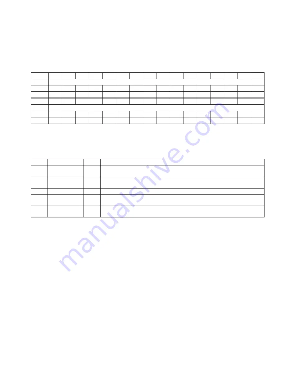
Bit

31

30

29

28

27

26

25

24

23

22

21

20

19

18

17

16

Name

TI extension base address

Type

RW

RW

RW

RW

RW

RW

RW

RW

RW

RW

RW

RW

RW

RW

RW

RW

Default

0

0

0

0

0

0

0

0

0

0

0

0

0

0

0

0

Bit

15

14

13

12

11

10

9

8

7

6

5

4

3

2

1

0

Name

TI extension base address

Type

RW

RW

R

R

R

R

R

R

R

R

R

R

R

R

R

R

Default

0

0

0

0

0

0

0

0

0

0

0

0

0

0

0

0

Register:

TI extension base address

Offset:

14h

Type:

Read/Write, Read-only

Default:

0000 0000h

Table 7−8. TI Base Address Register Description

BIT

FIELD NAME

TYPE

DESCRIPTION

31−14

TIREG_PTR

RW

TI register pointer. This field specifies the upper 18 bits of the 32-bit TI base address register. The
default value for this field is all 0s.

13−4

TI_SZ

R

TI register size. This field returns 0s when read, indicating that the TI registers require a 16K-byte
region of memory.

3

TI_PF

R

TI register prefetch. Bit 3 returns 0 when read, indicating that the TI registers are nonprefetchable.

2−1

TI_MEMTYPE

R

TI memory type. This field returns 0s when read, indicating that the TI base address register is 32 bits
wide and mapping can be done anywhere in the 32-bit memory space.

0

TI_MEM

R

TI memory indicator. Bit 0 returns 0 when read, indicating that the TI registers are mapped into system
memory space.

Summary of Contents for PCI7411

Page 1: ... June 2004 Connectivity Solutions Data Manual SCPS081 ...

Page 2: ...tute a license from TI to use such products or services or a warranty or endorsement thereof Use of such information may require a license from a third party under the patents or other intellectual property of the third party or a license from TI under the patents or other intellectual property of TI Reproduction of information in TI data books or data sheets is permissible only if reproduction is...

Page 3: ...stics 3 2 3 3 Clamping Voltages 3 2 3 4 Peripheral Component Interconnect PCI Interface 3 2 3 4 1 1394 PCI Bus Master 3 2 3 4 2 Device Resets 3 3 3 4 3 Serial EEPROM I2C Bus 3 3 3 4 4 Functions 0 and 1 CardBus Subsystem Identification 3 4 3 4 5 Function 2 OHCI 1394 Subsystem Identification 3 5 3 4 6 Function 3 Flash Media Subsystem Identification 3 5 3 4 7 Function 4 SD Host Subsystem Identificati...

Page 4: ...ower Management Overview 3 20 3 8 1 1394 Power Management Function 2 3 21 3 8 2 Integrated Low Dropout Voltage Regulator LDO VR 3 22 3 8 3 CardBus Functions 0 and 1 Clock Run Protocol 3 22 3 8 4 CardBus PC Card Power Management 3 22 3 8 5 16 Bit PC Card Power Management 3 23 3 8 6 Suspend Mode 3 23 3 8 7 Requirements for Suspend Mode 3 23 3 8 8 Ring Indicate 3 24 3 8 9 PCI Power Management 3 25 3 ...

Page 5: ... 11 4 19 CardBus Memory Base Registers 0 1 4 11 4 20 CardBus Memory Limit Registers 0 1 4 12 4 21 CardBus I O Base Registers 0 1 4 12 4 22 CardBus I O Limit Registers 0 1 4 13 4 23 Interrupt Line Register 4 13 4 24 Interrupt Pin Register 4 14 4 25 Bridge Control Register 4 15 4 26 Subsystem Vendor ID Register 4 16 4 27 Subsystem ID Register 4 17 4 28 PC Card 16 Bit I F Legacy Mode Base Address Reg...

Page 6: ...xCA I O Windows 0 and 1 Start Address High Byte Registers 5 13 5 11 ExCA I O Windows 0 and 1 End Address Low Byte Registers 5 14 5 12 ExCA I O Windows 0 and 1 End Address High Byte Registers 5 14 5 13 ExCA Memory Windows 0 4 Start Address Low Byte Registers 5 15 5 14 ExCA Memory Windows 0 4 Start Address High Byte Registers 5 16 5 15 ExCA Memory Windows 0 4 End Address Low Byte Registers 5 17 5 16...

Page 7: ...11 7 18 Capability ID and Next Item Pointer Registers 7 12 7 19 Power Management Capabilities Register 7 13 7 20 Power Management Control and Status Register 7 14 7 21 Power Management Extension Registers 7 14 7 22 PCI PHY Control Register 7 15 7 23 PCI Miscellaneous Configuration Register 7 16 7 24 Link Enhancement Control Register 7 17 7 25 Subsystem Access Register 7 18 7 26 GPIO Control Regist...

Page 8: ...hronous Cycle Timer Register 8 31 8 35 Asynchronous Request Filter High Register 8 32 8 36 Asynchronous Request Filter Low Register 8 34 8 37 Physical Request Filter High Register 8 35 8 38 Physical Request Filter Low Register 8 37 8 39 Physical Upper Bound Register Optional Register 8 37 8 40 Asynchronous Context Control Register 8 38 8 41 Asynchronous Context Command Pointer Register 8 39 8 42 I...

Page 9: ...er Registers 11 10 11 17 Power Management Capabilities Register 11 11 11 18 Power Management Control and Status Register 11 12 11 19 Power Management Bridge Support Extension Register 11 12 11 20 Power Management Data Register 11 13 11 21 General Control Register 11 13 11 22 Subsystem Access Register 11 14 11 23 Diagnostic Register 11 15 12 SD Host Controller Programming Model 12 1 12 1 Vendor ID ...

Page 10: ... 3 Command Register 13 3 13 4 Status Register 13 4 13 5 Class Code and Revision ID Register 13 5 13 6 Latency Timer and Class Cache Line Size Register 13 5 13 7 Header Type and BIST Register 13 6 13 8 Smart Card Base Address Register 0 13 6 13 9 Smart Card Base Address Register 1 4 13 7 13 10 Subsystem Vendor Identification Register 13 7 13 11 Subsystem Identification Register 13 8 13 12 Capabilit...

Page 11: ...mended Ranges of Operating Conditions 14 5 14 4 1 Device 14 5 14 4 2 Driver 14 5 14 4 3 Receiver 14 5 14 5 PCI Clock Reset Timing Requirements Over Recommended Ranges of Supply Voltage and Operating Free Air Temperature 14 6 14 6 Switching Characteristics for PHY Port Interface 14 6 14 7 Operating Timing and Switching Characteristics of XI 14 6 14 8 PCI Timing Requirements Over Recommended Ranges ...

Page 12: ...rotocol Byte Write 3 12 3 10 Serial Bus Protocol Byte Read 3 13 3 11 EEPROM Interface Doubleword Data Collection 3 13 3 12 IRQ Implementation 3 19 3 13 System Diagram Implementing CardBus Device Class Power Management 3 21 3 14 Signal Diagram of Suspend Function 3 23 3 15 RI_OUT Functional Diagram 3 24 3 16 Block Diagram of a Status Enable Cell 3 27 3 17 TP Cable Connections 3 30 3 18 Typical Comp...

Page 13: ...erminals 2 24 2 15 IEEE 1394 Physical Layer Terminals 2 26 2 16 SD MMC Terminals 2 27 2 17 Memory Stick PRO Terminals 2 27 2 18 Smart Media XD Terminals 2 28 2 19 Smart Card Terminals 2 29 3 1 PCI Bus Support 3 2 3 2 PC Card Card Detect and Voltage Sense Connections 3 7 3 3 TPS2228 Control Logic xVPP VCORE 3 8 3 4 TPS2228 Control Logic xVCC 3 8 3 5 TPS2226 Control Logic xVPP 3 8 3 6 TPS2226 Contro...

Page 14: ...tion 4 30 4 19 Power Management Capabilities Register Description 4 32 4 20 Power Management Control Status Register Description 4 33 4 21 Power Management Control Status Bridge Support Extensions Register Description 4 34 4 22 Serial Bus Data Register Description 4 35 4 23 Serial Bus Index Register Description 4 35 4 24 Serial Bus Slave Address Register Description 4 36 4 25 Serial Bus Control St...

Page 15: ...fication Register Description 7 9 7 11 Interrupt Line Register Description 7 10 7 12 PCI Interrupt Pin Register Read Only INTPIN Per Function 7 10 7 13 Minimum Grant and Maximum Latency Register Description 7 11 7 14 OHCI Control Register Description 7 11 7 15 Capability ID and Next Item Pointer Registers Description 7 12 7 16 Power Management Capabilities Register Description 7 13 7 17 Power Mana...

Page 16: ...t Filter High Register Description 8 35 8 30 Physical Request Filter Low Register Description 8 37 8 31 Asynchronous Context Control Register Description 8 38 8 32 Asynchronous Context Command Pointer Register Description 8 39 8 33 Isochronous Transmit Context Control Register Description 8 40 8 34 Isochronous Receive Context Control Register Description 8 41 8 35 Isochronous Receive Context Match...

Page 17: ... Interrupt Pin Register 12 9 12 9 Minimum Grant Register Description 12 9 12 10 Maximum Latency Register Description 12 10 12 11 Maximum Latency Register Description 12 10 12 12 Capability ID and Next Item Pointer Registers Description 12 11 12 13 Power Management Capabilities Register Description 12 12 12 14 Power Management Control and Status Register Description 12 13 12 15 General Control Regi...

Page 18: ...xviii Table Title Page 13 15 Smart Card Configuration 1 Register Description 13 16 13 16 Smart Card Configuration 2 Register Description 13 17 ...

Page 19: ... features that make it the best choice for bridging between the PCI bus and PC Cards and supports any combination of Smart Card Flash Media 16 bit CardBus and USB custom card interface PC Cards in the two sockets powered at 5 V or 3 3 V as required All card signals are internally buffered to allow hot insertion and removal without external buffering The PCI7621 controller is register compatible wi...

Page 20: ...r or through a dedicated Flash Media socket In addition this function includes DMA capabilities for improved Flash Media performance Function 4 of the PCI7421 controller is a PCI based SD host controller that supports MMC SD and SDIO cards This function controls communication with these Flash Media cards through a passive PC Card adapter or through a dedicated Flash Media socket In addition this f...

Page 21: ...e with data rates of 100 200 and 400 Mbits per second Deep FIFOs are provided to buffer 1394 data and accommodate large host bus latencies The PCI7411 controller provides physical write posting and a highly tuned physical data path for SBP 2 performance Function 3 of the PCI7411 controller is a PCI based Flash Media controller that supports Memory Stick Memory Stick Pro SmartMedia XD SD and MMC ca...

Page 22: ...errupt modes supported Serial ROM interface for loading subsystem ID and subsystem vendor ID ExCA compatible registers are mapped in memory or I O space Intel 82365SL DF register compatible Supports ring indicate SUSPEND and PCI CLKRUN protocols Provides VGA palette memory and I O and subtractive decoding options LED activity terminals Fully interoperable with FireWire and i LINK implementations o...

Page 23: ...al channels available registers PME support per 1394 Open Host Controller Interface Specification Advanced submicron low power CMOS technology 1 3 Related Documents Advanced Configuration and Power Interface ACPI Specification Revision 2 0 1394 Open Host Controller Interface Specification Release 1 1 IEEE Standard for a High Performance Serial Bus IEEE Std 1394 1995 IEEE Standard for a High Perfor...

Page 24: ...ormat Specification Sony Confidential ver 2 0 SmartMedia Standard 2000 May 19 2000 1 4 Trademarks Intel is a trademark of Intel Corporation TI and MicroStar BGA are trademarks of Texas Instruments FireWire is a trademark of Apple Computer Inc i LINK is a trademark of Sony Corporation of America Memory Stick is a trademark of Sony Kabushiki Kaisha TA Sony Corporation Japan Other trademarks are the ...

Page 25: ...erial peripheral interface a general purpose synchronous serial interface For more information see the Multimedia Card System Specification version 3 2 SSFDC Solid State Floppy Disk Card The SSFDC Forum specifies SmartMedia TI Smart Card driver A qualified software component provided by Texas Instruments that loads when an UltraMedia based Smart Card adapter is inserted into a PC Card slot This dr...

Page 26: ...1 8 ...

Page 27: ...5 A_CAD14 A_A9 A_CAD1 A_D4 B_CAD26 B_A0 B_CAD23 B_A3 B_CAD20 B_A6 B_CVS2 B_VS2 B_CAD18 B_A7 MS_DATA1 SD_DAT1 SM_D1 MS_CLK SD_CLK SM_EL_WP VCC VCC A_CSTOP A_A20 A_CAD15 A_IOWR VCC VCC VCC B_CAD21 B_A5 B_CC BE2 B_A12 B_CFRAME B_A23 B_CIRDY B_A15 SD_CLK SM_RE SC_GPIO1 SD_CMD SM_ALE SC_GPIO2 SM_R B SC_RFU GND GND VCC GND VCC B_CTRDY B_A22 B_CAD19 B_A25 B_CAD17 B_A24 B_CCLK B_A16 B_CDEVSEL B_A21 B_CGNT...

Page 28: ...A_CSTOP A_A20 A_CAD15 A_IOWR VCC VCC VCC B_CAD21 B_A5 B_CC BE2 B_A12 B_CFRAME B_A23 B_CIRDY B_A15 SD_CLK SM_RE SD_CMD SM_ALE SM_R B GND GND VCC GND VCC B_CTRDY B_A22 B_CAD19 B_A25 B_CAD17 B_A24 B_CCLK B_A16 B_CDEVSEL B_A21 B_CGNT B_WE SD_DAT2 SM_D6 SD_WP SM_CE RSVD SM_PHYS _WP VCC GND GND GND GND B_CPERR B_A14 B_CSTOP B_A20 B_CBLOCK B_A19 B_CPAR B_A13 VR_ PORT RSVD RSVD VR_ PORT SCL VCC GND GND GN...

Page 29: ...GPIO4 SD_WP SM_CE SC_RST SM_PHYS _WP SC_FCB VCC GND GND GND GND VR_ PORT SC_VCC _5V SC_CLK VR_ PORT SCL VCC GND GND GND VCC VR_EN CLK_48 SDA CLOCK MFUNC1 SPKROUT GND GND GND GND GND DATA LATCH MFUNC0 MFUNC5 VCC GND NC AGND VCC TEST0 VCC MFUNC2 MFUNC4 MFUNC3 GRST AD17 VCC PAR AD12 AD2 PC0 TEST1 SC_CD MFUNC6 SUSPEND PRST AD30 AD26 C BE1 CPS SC_OC RSVD PCLK GNT RI_OUT PME AD21 C BE2 DEVSEL AD11 AD6 A...

Page 30: ...PAR AD12 AD2 PC0 TEST1 MFUNC6 SUSPEND PRST AD30 AD26 C BE1 CPS RSVD PCLK GNT RI_OUT PME AD21 C BE2 DEVSEL AD11 AD6 AD1 AVDD AGND PHY_ TEST_ MA CNA REQ AD31 AD27 VSSPLL XI XO AD29 AD28 AD24 AD22 AD18 IRDY PERR AD14 VDPLL_ 33 C BE0 AD3 PC1 TEST2 VSSPLL TPBIAS0 AVDD VDPLL_ 15 VCCP AD25 IDSEL AD20 AD16 TRDY SERR AD13 AD10 AD8 AD4 PC2 TEST3 TPB0P TPA0P R1 TPB1P AVDD TPA1P TPBIAS1 C BE3 AD23 AD19 FRAME ...

Page 31: ...8 B_CCLKRUN B_WP IOIS16 D03 A_CAD29 A_D1 B01 A_CAD27 A_D0 D17 B_CAD26 B_A0 B02 A_CSTSCHG A_BVD1 STSCHG RI D18 B_CAD24 B_A2 B03 A_CSERR A_WAIT D19 VCCB VCCB B04 A_CAD26 A_A0 E01 B_USB_EN B_USB_EN B05 A_CAD23 A_A3 E02 A_USB_EN A_USB_EN B06 A_CAD21 A_A5 E03 SD_CD SD_CD B07 A_CAD18 A_A7 E05 A_CCD2 A_CD2 B08 A_CIRDY A_A15 E06 A_CAD24 A_A2 B09 A_CGNT A_WE E07 A_CREQ A_INPACK B10 A_CC BE1 A_A8 E08 A_CVS2...

Page 32: ...AT2 SM_D6 SC_GPIO4 G05 MS_CLK SD_CLK SM_EL_WP MS_CLK SD_CLK SM_EL_WP J02 SD_DAT3 SM_D7 SC_GPIO3 SD_DAT3 SM_D7 SC_GPIO3 G07 GND GND J03 SD_CMD SM_ALE SC_GPIO2 SD_CMD SM_ALE SC_GPIO2 G08 GND GND J05 SD_CLK SM_RE SC_GPIO1 SD_CLK SM_RE SC_GPIO1 G09 A_CAD20 A_A6 J06 SD_DAT1 SM_D5 SC_GPIO5 SD_DAT1 SM_D5 SC_GPIO5 G10 A_CPAR A_A13 J07 SM_CLE SC_GPIO0 SM_CLE SC_GPIO0 G11 A_CAD14 A_A9 J08 VCC VCC G12 A_CC B...

Page 33: ... L03 SC_OC SC_OC N18 B_CAD5 B_D6 L05 SC_PWR_CTRL SC_PWR_CTRL N19 B_CAD6 B_D13 L06 CLOCK CLOCK P01 MFUNC2 MFUNC2 L07 SPKROUT SPKROUT P02 MFUNC3 MFUNC3 L08 GND GND P03 MFUNC4 MFUNC4 L09 GND GND P05 PCLK PCLK L10 GND GND P06 AD20 AD20 L11 GND GND P09 PAR PAR L12 GND GND P12 TEST0 TEST0 L13 B_CAD15 B_IOWR P14 VSSPLL VSSPLL L15 B_CAD13 B_IORD P15 CNA CNA L17 B_CAD12 B_A11 P17 B_CAD1 B_D4 L18 B_CAD11 B_...

Page 34: ... TPB0P TPB0P U03 AD28 AD28 V15 TPA0P TPA0P U04 AD25 AD25 V16 TPB1P TPB1P U05 AD22 AD22 V17 AVDD AVDD U06 AD17 AD17 V18 TPA1P TPA1P U07 IRDY IRDY V19 VDPLL_33 VDPLL_33 U08 SERR SERR W02 AD27 AD27 U09 AD14 AD14 W03 VCCP VCCP U10 AD10 AD10 W04 C BE3 C BE3 U11 AD6 AD6 W05 IDSEL IDSEL U12 AD2 AD2 W06 AD19 AD19 U13 PC1 TEST2 PC1 TEST2 W07 C BE2 C BE2 U14 AGND AGND W08 STOP STOP U15 TPBIAS0 TPBIAS0 W09 C...

Page 35: ...A_CAD22 C06 B_CAD4 N15 B_CPAR K13 AD18 V06 A_CAD23 B05 B_CAD5 N18 B_CPERR J18 AD19 W06 A_CAD24 E06 B_CAD6 N19 B_CREQ E18 AD20 P06 A_CAD25 A04 B_CAD7 M15 B_CRST F17 AD21 R06 A_CAD26 B04 B_CAD8 M14 B_CSERR B18 AD22 U05 A_CAD27 B01 B_CAD9 M17 B_CSTOP J17 AD23 V05 A_CAD28 C02 B_CAD10 L19 B_CSTSCHG F14 AD24 V04 A_CAD29 D03 B_CAD11 L18 B_CTRDY H17 AD25 U04 A_CAD30 C01 B_CAD12 L17 B_CVS1 C18 AD26 V03 A_C...

Page 36: ...SCL M03 SM_CLE J07 VCC K08 GNT T02 SC_CD L02 SM_D0 G01 VCC K12 GRST T01 SC_CLK K05 SM_D1 G02 VCC M07 IDSEL W05 SC_DATA L01 SM_D2 G03 VCC M09 IRDY U07 SC_FCB K02 SM_D3 H05 VCC M10 LATCH N02 SC_GPIO0 J07 SM_D4 H03 VCC M12 MC_PWR_CTRL_0 F01 SC_GPIO1 J05 SM_D5 J06 VCC N07 MC_PWR_CTRL_1 F02 SC_GPIO2 J03 SM_D6 J01 VCCA A05 MFUNC0 N03 SC_GPIO3 J02 SM_D7 J02 VCCA A11 MFUNC1 M05 SC_GPIO4 J01 SM_EL_WP G05 V...

Page 37: ...6 A_A22 A08 B_A4 E19 B_D15 M14 AD18 V06 A_A23 C08 B_A5 G15 B_INPACK E18 AD19 W06 A_A24 A07 B_A6 F18 B_IORD L15 AD20 P06 A_A25 C07 B_A7 H15 B_IOWR L13 AD21 R06 A_BVD1 STSCHG RI B02 B_A8 K14 B_OE L18 AD22 U05 A_BVD2 SPKR A02 B_A9 K18 B_READY IREQ B19 AD23 V05 A_CD1 C15 B_A10 M17 B_REG F15 AD24 V04 A_CD2 E05 B_A11 L17 B_RESET F17 AD25 U04 A_CE1 G12 B_A12 G18 B_USB_EN E01 AD26 V03 A_CE2 B12 B_A13 K13 ...

Page 38: ...SCL M03 SM_CLE J07 VCC K08 GNT T02 SC_CD L02 SM_D0 G01 VCC K12 GRST T01 SC_CLK K05 SM_D1 G02 VCC M07 IDSEL W05 SC_DATA L01 SM_D2 G03 VCC M09 IRDY U07 SC_FCB K02 SM_D3 H05 VCC M10 LATCH N02 SC_GPIO0 J07 SM_D4 H03 VCC M12 MC_PWR_CTRL_0 F01 SC_GPIO1 J05 SM_D5 J06 VCC N07 MC_PWR_CTRL_1 F02 SC_GPIO2 J03 SM_D6 J01 VCCA A05 MFUNC0 N03 SC_GPIO3 J02 SM_D7 J02 VCCA A11 MFUNC1 M05 SC_GPIO4 J01 SM_EL_WP G05 V...

Page 39: ...t PCI output buffer LVCI1 LVCMOS input buffer LVCO1 Low noise 4 mA LVCMOS open drain output buffer LVCO2 Low noise 4 mA LVCMOS open drain output buffer LVCO3 Low noise 8 mA LVCMOS open drain output buffer PU PD signifies whether the terminal has an internal pullup or pulldown resistor These pullups are disabled and enabled by design when appropriate to preserve power PD1 20 µA failsafe pulldown PD...

Page 40: ...CP W03 W10 Clamp voltage for PCI and miscellaneous I O 5 V or 3 3 V PWR NA VDPLL_15 T18 1 5 V PLL circuit power terminal An external capacitor 0 1 µF recommended must be placed between terminals T18 and T17 VSSPLL when the internal voltage regulator is enabled VR_EN 0 V When the internal voltage regulator is disabled 1 5 V must be supplied to this terminal and a parallel combination of high freque...

Page 41: ...l causes the controller to place all output buffers in a high impedance state and reset all internal registers When GRST is asserted the controller is completely in its default state For systems that require wake up from D3 GRST is normally asserted only during initial boot PRST must be asserted following initial boot so that PME context is retained when transitioning from D3 to D0 For systems tha...

Page 42: ... data I O PCII3 PCIO3 VCCP C BE3 C BE2 C BE1 C BE0 W04 W07 W09 W11 PCI bus commands and byte enables These signals are multiplexed on the same PCI terminals During the address phase of a primary bus PCI cycle C BE3 C BE0 define the bus command During the data phase this 4 bit bus is used as byte enables The byte enables determine which byte paths of the full 32 bit data bus carry meaningful data C...

Page 43: ...transaction A data phase is completed on a rising edge of PCLK where both IRDY and TRDY are asserted Until IRDY and TRDY are both sampled asserted wait states are inserted I O PCII3 PCIO3 VCCP Pullup resistor per PCI specification PERR V08 PCI parity error indicator PERR is driven by a PCI controller to indicate that calculated parity does not match PAR when PERR is enabled through bit 6 of the co...

Page 44: ... per PCI specification NA RSVD T19 Reserved This terminal has no connection anywhere within the package Float SCL M03 Serial clock At PRST the SCL signal is sampled to determine if a two wire serial ROM is present If the serial ROM is detected then this terminal provides the serial clock signaling and is implemented as open drain For normal operation a ROM is implemented in the design this termina...

Page 45: ... B04 B_A25 B_A24 B_A23 B_A22 B_A21 B_A20 B_A19 B_A18 B_A17 B_A16 B_A15 B_A14 B_A13 B_A12 B_A11 B_A10 B_A9 B_A8 B_A7 B_A6 B_A5 B_A4 B_A3 B_A2 B_A1 B_A0 H14 G17 G19 H17 H19 J17 J19 K15 K17 H18 J13 J18 K13 G18 L17 M17 K18 K14 H15 F18 G15 E19 E17 D18 C19 D17 PC Card address 16 bit PC Card address lines A25 is the most significant bit O VCCA VCCB A_D15 A_D14 A_D13 A_D12 A_D11 A_D10 A_D9 A_D8 A_D7 A_D6 ...

Page 46: ...or the status bits for this signal Speaker SPKR is an optional binary audio signal available only when the card and socket have been configured for the 16 bit I O interface The audio signals from cards A and B are combined by the controller and are output on SPKROUT DMA request BVD2 can be used as the DMA request signal during DMA operations to a 16 bit PC Card that supports DMA The PC Card assert...

Page 47: ... DMA operations to a 16 bit PC Card that supports DMA The controller asserts REG to indicate a DMA operation REG is used in conjunction with the DMA read IOWR or DMA write IORD strobes to transfer data O VCCA VCCB A_RESET A06 B_RESET F17 PC Card reset RESET forces a hard reset to a 16 bit PC Card O VCCA VCCB A_VS1 A_VS2 A03 E08 B_VS1 B_VS2 C18 F19 Voltage sense 1 and voltage sense 2 VS1 and VS2 wh...

Page 48: ...rameters are defined with the rising edge of this signal CCLK operates at the PCI bus clock frequency but it can be stopped in the low state or slowed down for power savings O PCIO3 VCCA VCCB A_CCLKRUN C03 B_CCLKRUN A18 CardBus clock run CCLKRUN is used by a CardBus PC Card to request an increase in the CCLK frequency and by the controller to indicate that the CCLK frequency is going to be decreas...

Page 49: ...plexed CardBus address and data bus on the CardBus interface During the address phase of a CardBus cycle CAD31 CAD0 contain a 32 bit address During the data phase of a CardBus cycle CAD31 CAD0 contain data CAD31 is the most significant bit I O PCII7 PCIO7 VCCA VCCB A_CC BE3 A_CC BE2 A_CC BE1 A_CC BE0 C05 F09 B10 G12 B_CC BE3 B_CC BE2 B_CC BE1 B_CC BE0 F15 G18 K14 M18 CardBus bus commands and byte ...

Page 50: ...inue while this signal is asserted When CFRAME is deasserted the CardBus bus transaction is in the final data phase I O PCII7 PCIO7 VCCA VCCB A_CGNT B09 B_CGNT J15 CardBus bus grant CGNT is driven by the controller to grant a CardBus PC Card access to the CardBus bus after the current data transaction has been completed O PCII7 PCIO7 VCCA VCCB A_CINT C04 B_CINT B19 CardBus interrupt CINT is assert...

Page 51: ... the system to a change in the card status and is used as a wake up mechanism I PCII6 SW1 VCCA VCCB A_CTRDY A08 B_CTRDY H17 CardBus target ready CTRDY indicates the ability of the CardBus target to complete the current data phase of the transaction A data phase is completed on a rising edge of CCLK when both CIRDY and CTRDY are asserted until this time wait states are inserted I O PCII1 PCIO1 PU5 ...

Page 52: ...ation Float Pull directly to VCC TPA0P TPA0N V15 W15 Twisted pair cable A differential signal terminals Board trace lengths from each pair of positive and negative differential signal pins must be matched and as short as possible to the I O 1394 termination see reference schematics Float TPA1P TPA1N V18 W18 signal pins must be matched and as short as possible to the external load resistors and to ...

Page 53: ...te protect data This signal indicates that the media inserted in the socket is write protected I TTLI2 SW2 VCC Table 2 17 Memory Stick PRO Terminals If any Memory Stick PRO terminal is unused then the terminal may be left floating TERMINAL DESCRIPTION I O INPUT OUTPUT PU POWER EXTERNAL NAME NO DESCRIPTION I O TYPE INPUT OUTPUT PU PD POWER RAIL EXTERNAL COMPONENTS MC_PWR_CTRL_0 MC_PWR_CTRL_1 F01 F0...

Page 54: ...tch enable This signal functions as specified in the SmartMedia specification and is used to latch commands passed over SM_D7 SM_D0 O TTLO2 SW2 VCC SM_D7 SM_D6 SM_D5 SM_D4 SM_D3 SM_D2 SM_D1 SM_D0 J02 J01 J06 H03 H05 G03 G02 G01 SmartMedia data terminals These signals pass data to and from the SmartMedia and functions as specified in the SmartMedia specifications I O TTLI2 TTLO2 SW2 VCC SM_EL_WP G0...

Page 55: ...ontrol for the Smart Card socket O LVCO1 Power switch or FET to turn on power to FM socket SC_FCB K02 Smart Card function code The controller does not support synchronous Smart Cards as specified in ISO IEC 7816 10 and this terminal is in a high impedance state I PCII5 PCIO5 SW3 SC_GPIO6 SC_GPIO5 SC_GPIO4 SC_GPIO3 SC_GPIO2 SC_GPIO1 SC_GPIO0 H03 J06 J01 J02 J03 J05 J07 Smart Card general purpose I ...

Page 56: ...2 30 ...

Page 57: ...em Block Diagram 3 1 Power Supply Sequencing The PCI7x21 PCI7x11 controller contains 3 3 V I O buffers with 5 V tolerance requiring a core power supply and clamp voltages The core power supply is always 1 5 V The clamp voltages can be either 3 3 V or 5 V depending on the interface The following power up and power down sequences are recommended The power up sequence is 1 Power core 1 5 V 2 Apply th...

Page 58: ...ent Interconnect PCI Interface The PCI7x21 PCI7x11 controller is fully compliant with the PCI Local Bus Specification The PCI7x21 PCI7x11 controller provides all required signals for PCI master or slave operation and may operate in either a 5 V or 3 3 V signaling environment by connecting the VCCP terminals to the desired voltage level In addition to the mandatory PCI signals the PCI7x21 PCI7x11 c...

Page 59: ...ial EEPROM The PCI7x21 PCI7x11 controller is always the bus master and the EEPROM is always the slave Either device can drive the bus low but neither device drives the bus high The high level is achieved through the use of pullup resistors on the SCL and SDA signal lines The PCI7x21 PCI7x11 controller is always the source of the clock signal SCL System designers who wish to load register values wi...

Page 60: ...ctions 0 and 1 This doubleword register is used for system and option card mobile dock identification purposes and is required by some operating systems Implementation of this unique identifier register is a PC 99 PC 2001 requirement The PCI7x21 PCI7x11 controller offers two mechanisms to load a read only value into the subsystem registers The first mechanism relies upon the system BIOS providing ...

Page 61: ...ete description of the register contents 3 4 7 Function 4 SD Host Subsystem Identification The subsystem identification register is used for system and option card identification purposes This register can be initialized from the serial EEPROM or programmed via the subsystem access register at offset 8Ch in the PCI configuration space see Section 12 23 Subsystem Access Register See Table 12 16 for...

Page 62: ...If the 12V_SW_SEL bit is 1 TPS2226 is used then the 1 8 V CardBus card causes the XVCARD bit in the socket present state register to be set 3 5 3 UltraMedia Card Detection The PCI7x21 PCI7x11 controller is capable of detecting all the UltraMedia devices defined by the PCMCIA Proposal 0262 MultiMedia Cards Secure Digital Memory Stick devices and Smart Card devices The detection of these devices is ...

Page 63: ...nnect to CVS2 Connect to CCD1 Ground Reserved Reserved 3 5 4 Flash Media Card Detection The PCI7x21 PCI7x11 controller detects an MMC SD card insertion through the MC_CD_0 terminal When this terminal is 0 an MMC SD card is inserted in the socket The PCI7x21 PCI7x11 controller debounces the MC_CD_0 signal such that instability of the signal does not cause false card insertions The debounce time is ...

Page 64: ...VCC CONTROL SIGNALS OUTPUT V_AVCC BVCC CONTROL SIGNALS OUTPUT V_BVCC D8 SHDN D3 D2 OUTPUT V_AVCC D8 SHDN D6 D7 OUTPUT V_BVCC 1 0 0 0 V 1 0 0 0 V 1 0 1 3 3 V 1 0 1 3 3 V 1 1 0 5 V 1 1 0 5 V 1 1 1 0 V 1 1 1 0 V 0 X X Hi Z 0 X X Hi Z Table 3 5 TPS2226 Control Logic xVPP AVPP CONTROL SIGNALS OUTPUT V_AVPP BVPP CONTROL SIGNALS OUTPUT V_BVPP D8 SHDN D0 D1 D9 OUTPUT V_AVPP D8 SHDN D4 D5 D10 OUTPUT V_BVPP...

Page 65: ... output terminal SPKROUT Some audio chips may not support both modes on one terminal and may have a separate terminal for binary and PWM The PCI7x21 PCI7x11 implementation includes a signal for PWM CAUDPWM which can be routed to an MFUNC terminal Bit 2 AUD2MUX located in the card control register is programmed to route a CardBus CAUDIO PWM terminal to CAUDPWM See Section 4 36 Multifunction Routing...

Page 66: ...0h Reserved 14h 1Ch Socket power management 20h 3 5 11 48 MHz Clock Requirements The PCI7x21 PCI7x11 controller is designed to use an external 48 MHz clock connected to the CLK_48 terminal to provide the reference for an internal oscillator circuit This oscillator in turn drives a PLL circuit that generates the various clocks required for the flash media function Function 3 of the PCI7x21 PCI7x11 ...

Page 67: ...ed through a doubleword of PCI configuration space at offset B0h Table 3 8 lists the registers used to program a serial bus device through software Table 3 8 PCI7x21 PCI7x11 Registers Used to Program Serial Bus Devices PCI OFFSET REGISTER NAME DESCRIPTION B0h Serial bus data Contains the data byte to send on write commands or the received data byte on read commands B1h Serial bus index The content...

Page 68: ...ontrol Doubleword reads are performed by the serial EEPROM initialization circuitry upon a PCI reset and may not be generated under software control See Section 3 6 4 Serial Bus EEPROM Application for details on how the PCI7x21 PCI7x11 controller automatically loads the subsystem identification and other register defaults through a serial bus EEPROM Figure 3 9 illustrates a byte write The PCI7x21 ...

Page 69: ...s R W Data Byte 2 Data Byte 1 Data Byte 0 M P M M M Master Acknowledgement S P Start Stop Condition A Slave Acknowledgement Data Byte 3 M S 1 1 0 0 0 0 0 1 A Restart R W Slave Address Start Figure 3 11 EEPROM Interface Doubleword Data Collection 3 6 4 Serial Bus EEPROM Application When the PCI bus is reset and the serial bus interface is detected the PCI7x21 PCI7x11 controller attempts to read the...

Page 70: ...ction 1 byte 0 bit 2 0Eh PCI 81h system control byte 1 bits 7 6 0Fh Reserved nonloadable PCI 82h system control byte 2 10h PCI 83h system control byte 3 bits 7 2 0 11h PCI 8Ch MFUNC routing byte 0 12h PCI 8Dh MFUNC routing byte 1 13h PCI 8Eh MFUNC routing byte 2 14h PCI 8Fh MFUNC routing byte 3 15h PCI 90h retry status bits 7 6 16h PCI 91h card control bit 7 17h PCI 92h device control bits 6 5 3 0...

Page 71: ... 0 30h OHCI 29h GUIDLo byte 1 31h OHCI 2Ah GUIDLo byte 2 32h OHCI 2Bh GUIDLo byte 3 33h Checksum Reserved no bit loaded 34h PCI F5h Link_Enh byte 1 bits 7 6 5 4 35h PCI F0h PCI miscellaneous byte 0 bits 5 4 2 1 0 36h PCI F1h PCI miscellaneous byte 1 bits 7 3 2 1 0 37h Reserved 38h Reserved CardBus CIS pointer 39h Reserved 3Ah PCI ECh PCI PHY control bits 7 3 1 3Bh Flash media core function indicat...

Page 72: ... PCI7x21 PCI7x11 controller provides several interrupt signaling schemes to accommodate the needs of a variety of platforms The different mechanisms for dealing with interrupts in this controller are based on various specifications and industry standards The ExCA register set provides interrupt control for some 16 bit PC Card functions and the CardBus socket register set provides interrupt control...

Page 73: ...ardBus cards UltraMedia card Table 3 10 Interrupt Mask and Flag Registers CARD TYPE EVENT MASK FLAG 16 bit memory Battery conditions BVD1 BVD2 ExCA offset 05h 45h 805h bits 1 and 0 ExCA offset 04h 44h 804h bits 1 and 0 16 bit memory Wait states READY ExCA offset 05h 45h 805h bit 2 ExCA offset 04h 44h 804h bit 2 16 bit I O Change in card status STSCHG ExCA offset 05h 45h 805h bit 0 ExCA offset 04h ...

Page 74: ...ests that the socket VCC and VPP be powered Upon completion of this power up sequence the PCI7x21 PCI7x11 interrupt scheme can be used to notify the host system see Table 3 11 denoted by the power cycle complete event This interrupt source is considered a PCI7x21 PCI7x11 internal event because it depends on the completion of applying power to the socket rather than on a signal change at the PC Car...

Page 75: ...rt legacy 16 bit PC Card functions As an example suppose the six IRQs used by legacy PC Card applications are IRQ3 IRQ4 IRQ5 IRQ9 IRQ10 and IRQ15 The multifunction routing status register must be programmed to a value of 0A9F 5432h This value routes the MFUNC0 terminal to INTA signaling and routes the remaining terminals as illustrated in Figure 3 12 Not shown is that INTA must also be routed to t...

Page 76: ...to fit into a system maintenance interrupt SMI scheme SMI interrupts are generated by the PCI7x21 PCI7x11 controller when enabled after a write cycle to either the socket control register CB offset 10h see Section 6 5 of the CardBus register set or the ExCA power control register ExCA offset 02h 42h 802h see Section 5 3 causes a power cycle change sequence to be sent on the power switch interface ...

Page 77: ...ed interrupt events were interpreted as IntEvent n IntMask n IntMask masterIntEnable where n represents a specific interrupt event Based on feedback from Microsoft this implementation may cause problems with the existing Windows power management arcitecture as a PME and an interrupt could be simultaneously signaled on a transition from the D1 to D0 state where interrupts were enabled to generate w...

Page 78: ... 29 is set The 16 bit PC Card resource manager is busy The PCI7x21 PCI7x11 CardBus master state machine is busy A cycle may be in progress on CardBus The PCI7x21 PCI7x11 master is busy There may be posted data from CardBus to PCI in the PCI7x21 PCI7x11 controller Interrupts are pending The CardBus CCLK for the socket has not been stopped by the PCI7x21 PCI7x11 CCLKRUN manager Bit 0 KEEP_PCLK in th...

Page 79: ...eset signal from the PCI7x21 PCI7x11 controller Besides gating PRST and GRST SUSPEND also gates PCLK inside the PCI7x21 PCI7x11 controller in order to minimize power consumption It should also be noted that asynchronous signals such as card status change interrupts and RI_OUT can be passed to the host system without a PCI clock However if card status change interrupts are routed over the serial in...

Page 80: ...10 for a detailed description of CSC interrupt masks and flags Card I F PC Card Socket A CSC CSTSMASK RIENB RI_OUT RI_OUT Function RINGEN CDRESUME CSC RI PC Card Socket B Figure 3 15 RI_OUT Functional Diagram RI from the 16 bit PC Card interface is masked by bit 7 RINGEN in the ExCA interrupt and general control register ExCA offset 03h 43h 803h see Section 5 4 This is programmed on a per socket b...

Page 81: ...rom the device power state of the originating bridge device For the operating system OS to manage the controller power states on the PCI bus the PCI function must support four power management operations These operations are Capabilities reporting Power status reporting Setting the power state System wake up The OS identifies the capabilities of the PCI function by traversing the new capabilities ...

Page 82: ...ER NAME OFFSET Power management capabilities Next item pointer Capability ID 80h Data Power management control status register bridge support extensions Power management control status CSR 84h 3 8 9 5 Smart Card Function 5 Power Management The PCI Bus Power Management Interface Specification is applicable for the Smart Card dedicated sockets This function supports the D0 and D3 power states Table ...

Page 83: ... in the general purpose event status register PCI offset 88h see Section 4 32 and general purpose event enable register PCI offset 89h see Section 4 33 The status and enable bits are implemented as defined by ACPI and illustrated in Figure 3 16 Event Output Event Input Enable Bit Status Bit Figure 3 16 Block Diagram of a Status Enable Cell The status and enable bits generate an event that allows t...

Page 84: ...gister PCI offset 8Ch see Section 4 36 bits 31 0 Retry status register PCI offset 90h see Section 4 37 bits 7 5 3 1 Card control register PCI offset 91h see Section 4 38 bits 7 2 0 Device control register PCI offset 92h see Section 4 39 bits 7 5 3 0 Diagnostic register PCI offset 93h see Section 4 40 bits 7 0 Power management capabilities register PCI offset A2h see Section 4 43 bit 15 Power manag...

Page 85: ...egister PCI offset 2Ch see Section 12 9 bits 15 0 Subsystem ID register PCI offset 2Eh see Section 12 10 bits 15 0 Power management control and status register PCI offset 84h see Section 12 19 bits 15 8 1 0 General control register PCI offset 88h see Section 12 22 bits 6 4 0 Diagnostic register PCI offset 90h see Section 12 24 bits 31 0 The global reset only function 5 register bits Subsystem vend...

Page 86: ... PCI7x21 PCI7x11 Cable Power Pair Cable Pair A Cable Pair B Outer Shield Termination NOTE A IEEE Std 1394 1995 calls for a 250 pF capacitor which is a nonstandard component value A 220 pF capacitor is recommended Figure 3 17 TP Cable Connections 1 MΩ 0 001 µF 0 01 µF Outer Cable Shield Chassis Ground Figure 3 18 Typical Compliant DC Isolated Outer Shield Termination ...

Page 87: ...is recommended for adequate margin NOTE The total frequency variation must be kept below 100 ppm from nominal with some allowance for error introduced by board and device variations Trade offs between frequency tolerance and stability may be made as long as the total frequency variation is less than 100 ppm For example the frequency tolerance of the crystal may be specified at 50 ppm and the tempe...

Page 88: ...nd initialization sequence The IBR bit is located in PHY register 1 along with the root holdoff bit RHB and Gap_Count field as required by IEEE Std 1394a 2000 Therefore whenever the IBR bit is written the RHB and Gap_Count are also written The RHB and Gap_Count may also be updated by PHY config packets The PCI7x21 PCI7x11 controller is IEEE 1394a 2000 compliant and therefore both the reception and...

Page 89: ...o be loaded with the correct values consistent with the just transmitted PHY config packet In the PCI7x21 PCI7x11 controller the RHB and Gap_Count are updated to their correct values upon the transmission of the PHY config packet so these values may first be read from register 1 and then rewritten Other than to initiate the bus reset which must follow the transmission of a PHY config packet whenev...

Page 90: ...3 34 ...

Page 91: ...pear in the type column Table 4 1 describes the field access tags Table 4 1 Bit Field Access Tag Descriptions ACCESS TAG NAME MEANING R Read Field can be read by software W Write Field can be written by software to any value S Set Field can be set by a write of 1 Writes of 0 have no effect C Clear Field can be cleared by a write of 1 Writes of 0 have no effect U Update Field can be autonomously up...

Page 92: ...l status bridge support extensions Power management control status A4h Reserved A8h ACh Serial bus control status Serial bus slave address Serial bus index Serial bus data B0h Reserved B4h FCh One or more bits in this register are PME context bits and can be cleared only by the assertion of GRST when PME is enabled If PME is not enabled then this bit is cleared by the assertion of PRST or GRST One...

Page 93: ...TI to the PCI7x21 PCI7x11 CardBus controller functions PCI functions 0 and 1 Bit 15 14 13 12 11 10 9 8 7 6 5 4 3 2 1 0 Name Device ID Smart Card enabled Type R R R R R R R R R R R R R R R R Default 1 0 0 0 0 0 0 0 0 0 1 1 0 0 0 1 Register Device ID Offset 02h Functions 0 and 1 Type Read only Default 8031h ...

Page 94: ... PCI7x11 controller to report address parity errors 0 Disables the SERR output driver default 1 Enables the SERR output driver 7 RSVD R Reserved Bit 7 returns 0 when read 6 PERR_EN RW Parity error response enable This bit controls the PCI7x21 PCI7x11 response to parity errors through the PERR signal Data parity errors are indicated by asserting PERR while address parity errors are indicated by ass...

Page 95: ...t is set when SERR is enabled and the PCI7x21 PCI7x11 controller signaled a system error to the host Write a 1 to clear this bit 13 MABORT RW Received master abort This bit is set when a cycle initiated by the PCI7x21 PCI7x11 controller on the PCI bus has been terminated by a master abort Write a 1 to clear this bit 12 TABT_REC RW Received target abort This bit is set when a cycle initiated by the...

Page 96: ...1 PCI7x11 controller Bit 7 6 5 4 3 2 1 0 Name Revision ID Type R R R R R R R R Default 0 0 0 0 0 0 0 0 Register Revision ID Offset 08h functions 0 1 Type Read only Default 00h 4 7 Class Code Register The class code register recognizes PCI7x21 PCI7x11 functions 0 and 1 as a bridge device 06h and a CardBus bridge device 07h with a 00h programming interface Bit 23 22 21 20 19 18 17 16 15 14 13 12 11 ...

Page 97: ...pe Read Write Default 00h 4 10 Header Type Register The header type register returns 82h when read indicating that the PCI7x21 PCI7x11 functions 0 and 1 configuration spaces adhere to the CardBus bridge PCI header The CardBus bridge PCI header ranges from PCI registers 00h 7Fh and 80h FFh is user definable extension registers Bit 7 6 5 4 3 2 1 0 Name Header type Type R R R R R R R R Default 1 0 0 ...

Page 98: ... 24 23 22 21 20 19 18 17 16 Name CardBus socket registers ExCA base address Type RW RW RW RW RW RW RW RW RW RW RW RW RW RW RW RW Default 0 0 0 0 0 0 0 0 0 0 0 0 0 0 0 0 Bit 15 14 13 12 11 10 9 8 7 6 5 4 3 2 1 0 Name CardBus socket registers ExCA base address Type RW RW RW RW R R R R R R R R R R R R Default 0 0 0 0 0 0 0 0 0 0 0 0 0 0 0 0 Register CardBus socket registers ExCA base address Offset 1...

Page 99: ...RC Received target abort This bit is set when a cycle initiated by the PCI7x21 PCI7x11 controller on the CardBus bus is terminated by a target abort Write a 1 to clear this bit 11 SIG_CBTA RC Signaled target abort This bit is set by the PCI7x21 PCI7x11 controller when it terminates a transaction on the CardBus bus with a target abort Write a 1 to clear this bit 10 9 CB_SPEED R CDEVSEL timing These...

Page 100: ... this register in conjunction with the PCI bus number and subordinate bus number registers to determine when to forward PCI configuration cycles to its secondary buses This register is separate for each PCI7x21 PCI7x11 controller function Bit 7 6 5 4 3 2 1 0 Name CardBus bus number Type RW RW RW RW RW RW RW RW Default 0 0 0 0 0 0 0 0 Register CardBus bus number Offset 19h Type Read Write Default 0...

Page 101: ...rd a memory transaction to the CardBus bus and likewise when to forward a CardBus cycle to PCI Bits 31 12 of these registers are read write and allow the memory base to be located anywhere in the 32 bit PCI memory space on 4 Kbyte boundaries Bits 11 0 are read only and always return 0s Writes to these bits have no effect Bits 8 and 9 of the bridge control register PCI offset 3Eh see Section 4 25 s...

Page 102: ...t 0000 0000h 4 21 CardBus I O Base Registers 0 1 These registers indicate the lower address of a PCI I O address range They are used by the PCI7x21 PCI7x11 controller to determine when to forward an I O transaction to the CardBus bus and likewise when to forward a CardBus cycle to the PCI bus The lower 16 bits of this register locate the bottom of the I O window within a 64 Kbyte page The upper 16...

Page 103: ...1 Writes to read only bits have no effect These I O windows are enabled when either the I O base register or the I O limit register is nonzero By default the I O windows are not enabled to pass the first doubleword of I O to CardBus Either the I O base register or the I O limit register must be nonzero to enable any I O transactions Bit 31 30 29 28 27 26 25 24 23 22 21 20 19 18 17 16 Name I O limi...

Page 104: ...ly The internal interrupt connections set by INTRTIE and TIEALL are communicated to host software through this standard register interface This read only register is described for all PCI7x21 PCI7x11 functions in Table 4 6 PCI function 0 Bit 7 6 5 4 3 2 1 0 Name Interrupt pin PCI function 0 Type R R R R R R R R Default 0 0 0 0 0 0 0 1 PCI function 1 Bit 7 6 5 4 3 2 1 0 Name Interrupt pin PCI funct...

Page 105: ...RW RW RW RW RW RW R RW RW RW RW Default 0 0 0 0 0 0 1 1 0 1 0 0 0 0 0 0 Register Bridge control Offset 3Eh Function 0 1 Type Read only Read Write Default 0340h Table 4 7 Bridge Control Register Description BIT SIGNAL TYPE FUNCTION 15 11 RSVD R These bits return 0s when read 10 POSTEN RW Write posting enable Enables write posting to and from the CardBus sockets Write posting enables the posting of ...

Page 106: ...bit controls the response of the PCI7x21 PCI7x11 controller to CSERR signals on the CardBus bus This bit is separate for each socket 0 CSERR is not forwarded to PCI SERR default 1 CSERR is forwarded to PCI SERR 0 CPERREN RW CardBus parity error response enable This bit controls the response of the PCI7x21 PCI7x11 to CardBus parity errors This bit is separate for each socket 0 CardBus parity errors...

Page 107: ...index data scheme of accessing the ExCA registers which is mapped by this register An address written to this register is the address for the index register and the address 1 is the data address Using this access method applications requiring index data ExCA access can be supported The base address can be mapped anywhere in 32 bit I O space on a word boundary hence bit 0 is read only returning 1 w...

Page 108: ...NTD 28 TIEALL RW This bit ties INTA INTB INTC and INTD internally to INTA and reports this through the interrupt pin register PCI offset 3Dh see Section 4 24 27 PSCCLK RW P2C power switch clock The PCI7x21 PCI7x11 CLOCK signal clocks the serial interface power switch and the internal state machine The default state for this bit is 0 requiring an external clock source provided to the CLOCK terminal...

Page 109: ...mplete delay has expired default 1 Power stream is in progress 10 DELAYUP R Power up delay in progress status bit When set this bit indicates that a power up stream has been sent to the power switch and proper power may not yet be stable This bit is cleared when the power up delay has expired 0 Power up delay has expired default 1 Power up stream sent to switch Power might not be stable 9 DELAYDOW...

Page 110: ...e PME signal is routed to the PME RI_OUT terminal R03 When this bit is 0 and bit 7 RIENB of the card control register is 1 the RI_OUT signal is routed to the PME RI_OUT terminal If this bit is 0 and bit 7 RIENB of the card control register is 0 then the output is placed in a high impedance state This terminal is encoded as 0 RI_OUT signal is routed to the PME RI_OUT terminal if bit 7 of the card c...

Page 111: ...CI function and provides control over miscellaneous new functionality See Table 4 9 for a complete description of the register contents Bit 15 14 13 12 11 10 9 8 7 6 5 4 3 2 1 0 Name General control Type R R RW RW RW RW R R R R RW RW RW R RW RW Default 0 0 0 0 0 0 0 0 0 0 0 0 0 0 1 1 Register General control Offset 86h Type Read Write Read only Default 0003h ...

Page 112: ...able power switch TPS2226 is used 9 8 FM_IF_SEL RW Dedicated flash media interface selection This field controls the mode of the dedicated flash media interface 00 Flash media interface configured as SD MMC socket MS socket default 01 Flash media interface configured as 2 in 1 SD MMC MS socket 10 Flash media interface configured as 3 in 1 SD MMC MS SM XD socket 11 Reserved 7 DISABLE_SC RW When thi...

Page 113: ... This bit is set when software has changed the requested VPP level to or from 12 V for either socket 5 RSVD R Reserved This bit returns 0 when read A write has no effect 4 GP4_STS RCU GPI4 status This bit is set on a change in status of the MFUNC5 terminal input level if configured as a general purpose input GPI4 3 GP3_STS RCU GPI3 status This bit is set on a change in status of the MFUNC4 termina...

Page 114: ...ble When this bit is set GPE is signaled on GP1_STS events 0 GP0_EN RW GPI0 GPE enable When this bit is set GPE is signaled on GP0_STS events This bit is cleared only by the assertion of GRST 4 34 General Purpose Input Register The general purpose input register contains the logical value of the data input to the GPI terminals See Table 4 12 for a complete description of the register contents Bit ...

Page 115: ...Purpose Output Register Description BIT SIGNAL TYPE FUNCTION 7 5 RSVD R Reserved These bits return 0s when read Writes have no effect 4 GPO4_DATA RW This bit represents the logical value of the data driven to GPO4 3 GPO3_DATA RW This bit represents the logical value of the data driven to GPO3 2 GPO2_DATA RW This bit represents the logical value of the data driven to GPO2 1 GPO1_DATA RW This bit re...

Page 116: ...IRQ9 1101 IRQ13 0010 IRQ2 0110 IRQ6 1010 IRQ10 1110 IRQ14 0011 IRQ3 0111 IRQ7 1011 IRQ11 1111 IRQ15 23 20 MFUNC5 RW Multifunction terminal 5 configuration These bits control the internal signal mapped to the MFUNC5 terminal as follows 0000 GPI4 0100 SC_DBG_RX 1000 CAUDPWM 1100 LEDA1 0001 GPO4 0101 IRQ5 1001 IRQ9 1101 LED_SKT 0010 PCGNT 0110 RSVD 1010 FM_LED 1110 GPE 0011 IRQ3 0111 RSVD 1011 OHCI_L...

Page 117: ...riting a 1 to the bit Access this register only through function 0 See Table 4 15 for a complete description of the register contents Bit 7 6 5 4 3 2 1 0 Name Retry status Type RW RW RC R RC R RC R Default 1 1 0 0 0 0 0 0 Register Retry status Offset 90h Functions 0 1 Type Read only Read Write Read Clear Default C0h Table 4 15 Retry Status Register Description BIT SIGNAL TYPE FUNCTION 7 PCIRETRY R...

Page 118: ...dBus signal must be routed through an MFUNC terminal If this bit is set for both functions then function 0 is routed 0 CAUDIO set to CAUDPWM on MFUNC terminal default 1 CAUDIO is not routed 1 SPKROUTEN RW When bit 1 is set the SPKR terminal from the PC Card is enabled and is routed to tthe SPKROUT terminal The SPKR signal from socket 0 is XORed with the SPKR signal from socket 1 and sent to SPKROU...

Page 119: ... be necessary to lock socket power in order to support wake on LAN or RING if the operating system is programmed to power down a socket when the CardBus controller is placed in the D3 state 6 3VCAPABLE RW 3 V socket capable force bit 0 Not 3 V capable 1 3 V capable default 5 IO16R2 RW Diagnostic bit This bit defaults to 1 4 RSVD R Reserved This bit returns 0 when read A write has no effect 3 TEST ...

Page 120: ...ult 1 Returns all 1s to reads from the PCI vendor ID and PCI device ID registers 6 RSVD R Reserved This bit is read only and returns 1 when read 5 CSC RW CSC interrupt routing control 0 CSC interrupts routed to PCI if ExCA 803 bit 4 1 1 CSC interrupts routed to PCI if ExCA 805 bits 7 4 0000b default In this case the setting of ExCA 803 bit 4 is a don t care 4 DIAG4 RW Diagnostic RETRY_DIS Delayed ...

Page 121: ... ID Type R R R R R R R R Default 0 0 0 0 0 0 0 1 Register Capability ID Offset A0h Type Read only Default 01h 4 42 Next Item Pointer Register The contents of this register indicate the next item in the linked list of the PCI power management capabilities Because the PCI7x21 PCI7x11 functions only include one capabilities item this register returns 0s when read Bit 7 6 5 4 3 2 1 0 Name Next item po...

Page 122: ...ue 1 to indicate that the PME signal can be asserted from the D3hot state Bit 13 contains the value 1 to indicate that the PME signal can be asserted from the D2 state Bit 12 contains the value 1 to indicate that the PME signal can be asserted from the D1 state Bit 11 contains the value 1 to indicate that the PME signal can be asserted from the D0 state 10 D2_Support R This bit returns a 1 when re...

Page 123: ...e CardBus function would normally assert the PME signal independent of the state of the PME_EN bit This bit is cleared by a writeback of 1 and this also clears the PME signal if PME was asserted by this function Writing a 0 to this bit has no effect 14 13 DATASCALE R This 2 bit field returns 0s when read The CardBus function does not return any dynamic data 12 9 DATASEL R Data select This 4 bit fi...

Page 124: ...When the bus power clock control enable mechanism is disabled the power state field bits 1 0 of the power management control status register PCI offset A4h see Section 4 44 cannot be used by the system software to control the power or the clock of the secondary bus A 1 indicates that the bus power clock control mechanism is enabled 6 B2_B3 R B2 B3 support for D3hot The state of this bit determines...

Page 125: ...ace On reads the REQBUSY bit must be polled to verify that the contents of this register are valid These bits are cleared only by the assertion of GRST 4 48 Serial Bus Index Register The serial bus index register is for programmable serial bus byte reads and writes This register represents the byte address when generating cycles on the serial bus interface To write a byte the serial bus data regis...

Page 126: ... Then the contents of the serial bus data register are valid read data from the serial bus interface See Table 4 24 for a complete description of the register contents Bit 7 6 5 4 3 2 1 0 Name Serial bus slave address Type RW RW RW RW RW RW RW RW Default 0 0 0 0 0 0 0 0 Register Serial bus slave address Offset B2h function 0 Type Read Write Default 00h Table 4 24 Serial Bus Slave Address Register ...

Page 127: ...BUSY R Serial EEPROM busy status Bit 4 indicates the status of the PCI7x21 PCI7x11 serial EEPROM circuitry Bit 4 is set during the loading of the subsystem ID and other default values from the serial bus EEPROM 0 Serial EEPROM circuitry is not busy 1 Serial EEPROM circuitry is busy 3 SBDETECT RW Serial bus detect When the serial bus interface is detected through a pullup resistor on the SCL termin...

Page 128: ...4 38 ...

Page 129: ... and 1 This illustration also identifies the CardBus socket register mapping which is mapped into the same 4K window at memory offset 0h The interrupt registers in the ExCA register set as defined by the 82365SL specification control such card functions as reset type interrupt routing and interrupt enables Special attention must be paid to the interrupt routing registers and the host interrupt sig...

Page 130: ...cation is returned in the data register Offset Figure 5 1 ExCA Register Access Through I O 16 Bit Legacy Mode Base Address CardBus Socket ExCA Base Address 10h 44h CardBus Socket A Registers ExCA Registers Card A 20h 800h 844h Host Memory Space CardBus Socket B Registers ExCA Registers Card B 20h 800h 844h Host Memory Space Note The CardBus socket ExCA base address mode register is separate for fu...

Page 131: ...2 12 52 Memory window 0 end address high byte 813 13 53 Memory window 0 offset address low byte 814 14 54 Memory window 0 offset address high byte 815 15 55 Card detect and general control 816 16 56 Reserved 817 17 57 Memory window 1 start address low byte 818 18 58 Memory window 1 start address high byte 819 19 59 Memory window 1 end address low byte 81A 1A 5A Memory window 1 end address high byt...

Page 132: ... low byte 830 30 70 Memory window 4 start address high byte 831 31 71 Memory window 4 end address low byte 832 32 72 Memory window 4 end address high byte 833 33 73 Memory window 4 offset address low byte 834 34 74 Memory window 4 offset address high byte 835 35 75 I O window 0 offset address low byte 836 36 76 I O window 0 offset address high byte 837 37 77 I O window 1 offset address low byte 83...

Page 133: ...ad only Default 84h Table 5 2 ExCA Identification and Revision Register Description BIT SIGNAL TYPE FUNCTION 7 6 IFTYPE R Interface type These bits which are hardwired as 10b identify the 16 bit PC Card support provided by the PCI7x21 PCI7x11 controller The PCI7x21 PCI7x11 controller supports both I O and memory 16 bit PC Cards 5 4 RSVD RW These bits can be used for 82365SL emulation 3 0 365REV RW...

Page 134: ...l reports to the PCI7x21 PCI7x11 controller whether or not the memory card is write protected Further write protection for an entire PCI7x21 PCI7x11 16 bit memory window is available by setting the appropriate bit in the ExCA memory window offset address high byte register 0 WP signal is 0 PC Card is R W 1 WP signal is 1 PC Card is read only 3 CDETECT2 R Card detect 2 This bit indicates the status...

Page 135: ...3 and 2 return 0s when read 1 0 EXCAVPP RW PC Card VPP power control Bits 1 and 0 are used to request changes to card VPP The PCI7x21 PCI7x11 controller ignores this field unless VCC to the socket is enabled This field is encoded as 00 No connection default 10 12 V 01 VCC 11 Reserved One or more bits in this register are cleared only by the assertion of GRST when PME is enabled If PME is not enabl...

Page 136: ...it This bit has meaning only if the CSC interrupt routing control bit PCI offset 93h bit 5 is 0 In this case when this bit is set high the card status change interrupts are routed to PCI interrupts When low the card status change interrupts are routed using bits 7 4 in the ExCA card status change interrupt configuration register ExCA offset 805h see Section 5 6 This bit is encoded as 0 CSC interru...

Page 137: ...ed Bits 7 4 return 0s when read 3 CDCHANGE R Card detect change Bit 3 indicates whether a change on CD1 or CD2 occurred at the PC Card interface This bit is encoded as 0 No change detected on either CD1 or CD2 1 Change detected on either CD1 or CD2 2 READYCHANGE R Ready change When a 16 bit memory is installed in the socket bit 2 includes whether the source of a PCI7x21 PCI7x11 interrupt was due t...

Page 138: ...010 SMI enabled 0011 IRQ3 enabled 0100 IRQ4 enabled 0101 IRQ5 enabled 0110 IRQ6 enabled 0111 IRQ7 enabled 1000 IRQ8 enabled 1001 IRQ9 enabled 1010 IRQ10 enabled 1011 IRQ11 enabled 1100 IRQ12 enabled 1101 IRQ13 enabled 1110 IRQ14 enabled 1111 IRQ15 enabled 3 CDEN RW Card detect enable Enables interrupts on CD1 or CD2 changes This bit is encoded as 0 Disables interrupts on CD1 or CD2 line changes de...

Page 139: ...as 0 I O window 1 disabled default 1 I O window 1 enabled 6 IOWIN0EN RW I O window 0 enable Bit 6 enables disables I O window 0 for the PC Card This bit is encoded as 0 I O window 0 disabled default 1 I O window 0 enabled 5 RSVD R Reserved Bit 5 returns 0 when read 4 MEMWIN4EN RW Memory window 4 enable Bit 4 enables disables memory window 4 for the PC Card This bit is encoded as 0 Memory window 4 ...

Page 140: ...idth of the I O data transfer This bit is encoded as 0 Window data width determined by DATASIZE1 bit 4 default 1 Window data width determined by IOIS16 4 DATASIZE1 RW I O window 1 data size Bit 4 controls the I O window 1 data size Bit 4 is ignored if bit 5 IOSIS16W1 is set This bit is encoded as 0 Window data width is 8 bits default 1 Window data width is 16 bits 3 WAITSTATE0 RW I O window 0 wait...

Page 141: ...ardBus Socket Address 80Ch Card A ExCA Offset 0Ch Card B ExCA Offset 4Ch Type Read Write Default 00h 5 10 ExCA I O Windows 0 and 1 Start Address High Byte Registers These registers contain the high byte of the 16 bit I O window start address for I O windows 0 and 1 The 8 bits of these registers correspond to the upper 8 bits of the start address Bit 7 6 5 4 3 2 1 0 Name ExCA I O windows 0 and 1 st...

Page 142: ...CardBus Socket Address 80Eh Card A ExCA Offset 0Eh Card B ExCA Offset 4Eh Type Read Write Default 00h 5 12 ExCA I O Windows 0 and 1 End Address High Byte Registers These registers contain the high byte of the 16 bit I O window end address for I O windows 0 and 1 The 8 bits of these registers correspond to the upper 8 bits of the end address Bit 7 6 5 4 3 2 1 0 Name ExCA I O windows 0 and 1 end add...

Page 143: ...et CardBus Socket Address 810h Card A ExCA Offset 10h Card B ExCA Offset 50h Register ExCA memory window 1 start address low byte Offset CardBus Socket Address 818h Card A ExCA Offset 18h Card B ExCA Offset 58h Register ExCA memory window 2 start address low byte Offset CardBus Socket Address 820h Card A ExCA Offset 20h Card B ExCA Offset 60h Register ExCA memory window 3 start address low byte Of...

Page 144: ...set 61h Register ExCA memory window 3 start address high byte Offset CardBus Socket Address 829h Card A ExCA Offset 29h Card B ExCA Offset 69h Register ExCA memory window 4 start address high byte Offset CardBus Socket Address 831h Card A ExCA Offset 31h Card B ExCA Offset 71h Type Read Write Default 00h Table 5 11 ExCA Memory Windows 0 4 Start Address High Byte Registers Description BIT SIGNAL TY...

Page 145: ...t CardBus Socket Address 812h Card A ExCA Offset 12h Card B ExCA Offset 52h Register ExCA memory window 1 end address low byte Offset CardBus Socket Address 81Ah Card A ExCA Offset 1Ah Card B ExCA Offset 5Ah Register ExCA memory window 2 end address low byte Offset CardBus Socket Address 822h Card A ExCA Offset 22h Card B ExCA Offset 62h Register ExCA memory window 3 end address low byte Offset Ca...

Page 146: ...h Card B ExCA Offset 5Bh Register ExCA memory window 2 end address high byte Offset CardBus Socket Address 823h Card A ExCA Offset 23h Card B ExCA Offset 63h Register ExCA memory window 3 end address high byte Offset CardBus Socket Address 82Bh Card A ExCA Offset 2Bh Card B ExCA Offset 6Bh Register ExCA Memory window 4 end address high byte Offset CardBus Socket Address 833h Card A ExCA Offset 33h...

Page 147: ...set CardBus Socket Address 814h Card A ExCA Offset 14h Card B ExCA Offset 54h Register ExCA memory window 1 offset address low byte Offset CardBus Socket Address 81Ch Card A ExCA Offset 1Ch Card B ExCA Offset 5Ch Register ExCA memory window 2 offset address low byte Offset CardBus Socket Address 824h Card A ExCA Offset 24h Card B ExCA Offset 64h Register ExCA memory window 3 offset address low byt...

Page 148: ...ow 2 offset address high byte Offset CardBus Socket Address 825h Card A ExCA Offset 25h Card B ExCA Offset 65h Register ExCA memory window 3 offset address high byte Offset CardBus Socket Address 82Dh Card A ExCA Offset 2Dh Card B ExCA Offset 6Dh Register ExCA memory window 4 offset address high byte Offset CardBus Socket Address 835h Card A ExCA Offset 35h Card B ExCA Offset 75h Type Read Write D...

Page 149: ...nable bit is cleared to 0 in the ExCA card status change interrupt configuration register ExCA offset 805h see Section 5 6 then writing a 1 to the software card detect interrupt bit has no effect This bit is write only A read operation of this bit always returns 0 Writing a 1 to this bit also clears it If bit 2 of the ExCA global control register ExCA offset 81Eh see Section 5 20 is set and a 1 is...

Page 150: ...as 0 Host interrupt is edge mode default 1 Host interrupt is level mode 2 IFCMODE RW Interrupt flag clear mode select This bit selects the interrupt flag clear mechanism for the flags in the ExCA card status change register This bit is encoded as 0 Interrupt flags cleared by read of CSC register default 1 Interrupt flags cleared by explicit writeback of 1 1 CSCMODE RW Card status change level edge...

Page 151: ...fset CardBus Socket Address 838h Card A ExCA Offset 38h Card B ExCA Offset 78h Type Read Write Read only Default 00h 5 22 ExCA I O Windows 0 and 1 Offset Address High Byte Registers These registers contain the high byte of the 16 bit I O window offset address for I O windows 0 and 1 The 8 bits of these registers correspond to the upper 8 bits of the offset address Bit 7 6 5 4 3 2 1 0 Name ExCA I O...

Page 152: ...alue host software can locate 16 bit memory windows in any one of 256 16 Mbyte regions in the 4 gigabyte PCI address space These registers are only accessible when the ExCA registers are memory mapped that is these registers may not be accessed using the index data I O scheme Bit 7 6 5 4 3 2 1 0 Name ExCA memory windows 0 4 page Type RW RW RW RW RW RW RW R Default 0 0 0 0 0 0 0 0 Register ExCA mem...

Page 153: ...ss CardBus Socket ExCA Base Address 10h 44h CardBus Socket A Registers ExCA Registers Card A 20h 800h 844h Host Memory Space CardBus Socket B Registers ExCA Registers Card B 20h 800h 844h Host Memory Space Note The CardBus socket ExCA base address mode register is separate for functions 0 and 1 address register s base address Offsets are from the CardBus socket ExCA base 00h 00h PCI7x21 PCI7x11 Co...

Page 154: ... 0 0 0 0 0 0 0 0 0 0 Register Socket event Offset CardBus Socket Address 00h Type Read only Read Write to Clear Default 0000 0000h Table 6 2 Socket Event Register Description BIT SIGNAL TYPE FUNCTION 31 4 RSVD R These bits return 0s when read 3 PWREVENT RWC Power cycle This bit is set when the PCI7x21 PCI7x11 controller detects that the PWRCYCLE bit in the socket present state register offset 08h ...

Page 155: ... R These bits return 0s when read 3 PWRMASK RW Power cycle This bit masks the PWRCYCLE bit in the socket present state register offset 08h see Section 6 3 from causing a status change interrupt 0 PWRCYCLE event does not cause a CSC interrupt default 1 PWRCYCLE event causes a CSC interrupt 2 1 CDMASK RW Card detect mask These bits mask the CDETECT1 and CDETECT2 bits in the socket present state regi...

Page 156: ... 4 This bit defaults to 0 29 3VSOCKET R 3 V socket This bit indicates whether or not the socket can supply VCC 3 3 Vdc to PC Cards The PCI7x21 PCI7x11 controller does support 3 3 V VCC therefore this bit is always set unless overridden by the socket force event register offset 0Ch see Section 6 4 28 5VSOCKET R 5 V socket This bit indicates whether or not the socket can supply VCC 5 Vdc to PC Cards...

Page 157: ...ncoded as 0 Socket is powered down default 1 Socket is powered up 2 CDETECT2 R CCD2 This bit reflects the current status of the CCD2 signal at the PC Card interface Changes to this signal during card interrogation are not reflected here 0 CCD2 is low PC Card may be present 1 CCD2 is high PC Card not present 1 CDETECT1 R CCD1 This bit reflects the current status of the CCD1 signal at the PC Card in...

Page 158: ... cause the DATALOST bit in the socket present state register offset 08h see Section 6 3 to be written 7 FNOTACARD W Force not a card Writes to this bit cause the NOTACARD bit in the socket present state register offset 08h see Section 6 3 to be written 6 RSVD R This bit returns 0 when read 5 FCBCARD W Force CardBus card Writes to this bit cause the CBCARD bit in the socket present state register o...

Page 159: ...clock run state machine decides when to stop the CardBus clock to the CardBus card 0 The CardBus CLKRUN protocol can only attempt to stop slow the CaredBus clock if the sockethas been idle for 8 clocks and the PCI CLKRUN protocol is preparing to stop slow the PCI bus clock 1 The CardBus CLKRUN protocol can only attempt to stop slow the CaredBus clock if the socket has been idle for 8 clocks regard...

Page 160: ...hen read 25 SKTACCES R Socket access status This bit provides information on whether a socket access has occurred This bit is cleared by a read access 0 No PC Card access has occurred default 1 PC Card has been accessed 24 SKTMODE R Socket mode status This bit provides clock mode information 0 Normal clock operation 1 Clock frequency has changed 23 17 RSVD R These bits return 0s when read 16 CLKCT...

Page 161: ...andard header Table 7 1 illustrates the configuration header that includes both the predefined portion of the configuration space and the user definable registers Table 7 1 Function 2 Configuration Register Map REGISTER NAME OFFSET Device ID Vendor ID 00h Status Command 04h Class code Revision ID 08h BIST Header type Latency timer Cache line size 0Ch OHCI base address 10h TI extension base address...

Page 162: ... Default 0 0 0 1 0 0 0 0 0 1 0 0 1 1 0 0 Register Vendor ID Offset 00h Type Read only Default 104Ch 7 2 Device ID Register The device ID register contains a value assigned to the PCI7x21 PCI7x11 controller by Texas Instruments The device identification for the PCI7x21 PCI7x11 controller is 8032h Bit 15 14 13 12 11 10 9 8 7 6 5 4 3 2 1 0 Name Device ID Type R R R R R R R R R R R R R R R R Default 1...

Page 163: ...r this bit is 0 7 RSVD R Reserved Bit 7 returns 0 when read 6 PERR_ENB RW Parity error enable When bit 6 is set to 1 the PCI7x21 PCI7x11 controller is enabled to drive PERR response to parity errors through the PERR signal The default value for this bit is 0 5 VGA_ENB R VGA palette snoop enable The PCI7x21 PCI7x11 controller does not feature VGA palette snooping therefore bit 5 returns 0 when read...

Page 164: ...EED R DEVSEL timing Bits 10 and 9 encode the timing of DEVSEL and are hardwired to 01b indicating that the PCI7x21 PCI7x11 controller asserts this signal at a medium speed on nonconfiguration cycle accesses 8 DATAPAR RCU Data parity error detected Bit 8 is set to 1 when the following conditions have been met a PERR was asserted by any PCI device including the PCI7x21 PCI7x11 controller b The PCI7x...

Page 165: ...EV R Silicon revision This field returns 00h when read which indicates the silicon revision of the PCI7x21 PCI7x11 controller 7 6 Latency Timer and Class Cache Line Size Register The latency timer and class cache line size register is programmed by host BIOS to indicate system cache line size and the latency timer associated with the PCI7x21 PCI7x11 controller See Table 7 5 for a complete descript...

Page 166: ...r the OHCI registers See Table 7 7 for a complete description of the register contents Bit 31 30 29 28 27 26 25 24 23 22 21 20 19 18 17 16 Name OHCI base address Type RW RW RW RW RW RW RW RW RW RW RW RW RW RW RW RW Default 0 0 0 0 0 0 0 0 0 0 0 0 0 0 0 0 Bit 15 14 13 12 11 10 9 8 7 6 5 4 3 2 1 0 Name OHCI base address Type RW RW RW RW RW R R R R R R R R R R R Default 0 0 0 0 0 0 0 0 0 0 0 0 0 0 0 ...

Page 167: ...0 0 0 0 0 0 0 0 0 0 0 0 0 Register TI extension base address Offset 14h Type Read Write Read only Default 0000 0000h Table 7 8 TI Base Address Register Description BIT FIELD NAME TYPE DESCRIPTION 31 14 TIREG_PTR RW TI register pointer This field specifies the upper 18 bits of the 32 bit TI base address register The default value for this field is all 0s 13 4 TI_SZ R TI register size This field ret...

Page 168: ...ize This field returns 0s when read indicating that the CIS space requires a 2K byte region of memory 3 CIS_PF R CIS prefetch Bit 3 returns 0 when read indicating that the CIS is nonprefetchable Furthermore the CIS is a byte accessible address space and either a doubleword or 16 bit word access yields indeterminate results 2 1 CIS_MEMTYPE R CIS memory type This field returns 0s when read indicatin...

Page 169: ...entification Offset 2Ch Type Read Update Default 0000 0000h Table 7 10 Subsystem Identification Register Description BIT FIELD NAME TYPE DESCRIPTION 31 16 OHCI_SSID RU Subsystem device ID This field indicates the subsystem device ID 15 0 OHCI_SSVID RU Subsystem vendor ID This field indicates the subsystem vendor ID These bits are cleared only by the assertion of GRST 7 13 Power Management Capabili...

Page 170: ...ternal interrupt connections set by INTRTIE and TIEALL are communicated to host software through this standard register interface This read only register is described for all PCI7x21 PCI7x11 functions in Table 7 12 Bit 7 6 5 4 3 2 1 0 Name Interrupt pin Type R R R R R R R R Default 0 0 0 0 0 0 1 0 Register Interrupt pin Offset 3Dh Type Read only Default 02h Table 7 12 PCI Interrupt Pin Register Re...

Page 171: ...ough the serial EEPROM 7 0 MIN_GNT RU Minimum grant The contents of this field may be used by host BIOS to assign a latency timer register value to the PCI7x21 PCI7x11 controller The default for this register indicates that the PCI7x21 PCI7x11 controller may need to sustain burst transfers for nearly 64 µs and thus request a large value be programmed in bits 15 8 of the PCI7x21 PCI7x11 latency tim...

Page 172: ... 0 0 0 0 0 0 0 0 0 0 0 0 0 1 Register Capability ID and next item pointer Offset 44h Type Read only Default 0001h Table 7 15 Capability ID and Next Item Pointer Registers Description BIT FIELD NAME TYPE DESCRIPTION 15 8 NEXT_ITEM R Next item pointer The PCI7x21 PCI7x11 controller supports only one additional capability that is communicated to the system through the extended capabilities list there...

Page 173: ...support This 4 bit field indicates the power states from which the PCI7x21 PCI7x11 controller may assert PME This field returns a value of 1111b by default indicating that PME may be asserted from the D3hot D2 D1 and D0 power states 10 D2_SUPPORT R D2 support Bit 10 is hardwired to 1 indicating that the PCI7x21 PCI7x11 controller supports the D2 power state 9 D1_SUPPORT R D1 support Bit 9 is hardw...

Page 174: ...a register is not implemented 8 PME_ENB RW When bit 8 is set to 1 PME assertion is enabled When bit 8 is cleared PME assertion is disabled This bit defaults to 0 if the function does not support PME generation from D3cold If the function supports PME from D3cold then this bit is sticky and must be explicitly cleared by the operating system each time it is initially loaded 7 2 RSVD R Reserved Bits ...

Page 175: ...st be 1 for normal operation 6 5 RSVD R Reserved Bits 6 5 return 0s when read These bits must be 0s for normal operation 4 PHYRST RW PHY reset This bit controls the RST input to the PHY When bit 4 is set the PHY reset is asserted The default value is 0 This bit must be 0 for normal operation 3 RSVD RW Reserved Bit 3 defaults to 1 to indicate compliance with IEEE Std 1394a 2000 This bit is loaded v...

Page 176: ...havior generated from unmasked interrupt bits and IntMask masterIntEnable bit default 1 PME generation does not depend on the value of IntMask masterIntEnable 9 8 MR_ENHANCE RW This field selects the read command behavior of the PCI master for read transactions of greater than two data phases For read transactions of one or two data phases a memory read command is used The default of this field is...

Page 177: ...lining is disabled The default value for this bit is 0 14 RSVD R Reserved Bit 14 defaults to 0 and must remain 0 for normal operation of the OHCI core 13 12 atx_thresh RW This field sets the initial AT threshold value which is used until the AT FIFO is underrun When the PCI7x21 PCI7x11 controller retries the packet it uses a 2K byte threshold resulting in a store and forward operation 00 Threshold...

Page 178: ...ion enhancements OHCI Lynx compatible When bit 1 is set to 1 the PHY layer is notified that the link supports the IEEE Std 1394a 2000 acceleration enhancements that is ack accelerated fly by concatenation etc It is recommended that this bit be set to 1 The default value for this bit is 0 0 RSVD R Reserved Bit 0 returns 0 when read This bit is cleared only by the assertion of GRST 7 25 Subsystem Ac...

Page 179: ...output polarity control of GPIO3 0 Noninverted default 1 Inverted 28 GPIO_ENB3 R W GPIO3 enable control This bit controls the output enable for GPIO3 0 High impedance output default 1 Output is enabled 27 25 RSVD R Reserved Bits 27 25 return 0s when read 24 GPIO_DATA3 R W GPIO3 data When GPIO3 output is enabled the value written to this bit represents the logical data driven to the GPIO3 terminal ...

Page 180: ...anager contender BMC This bit configures this terminal as bus manager contender or GPIO0 0 BMC default 1 GPIO0 6 RSVD R Reserved Bit 6 returns 0 when read 5 GPIO_INV0 R W GPIO0 polarity invert When bit 7 DISABLE_BMC is set to 1 this bit controls the input output polarity control for GPIO0 0 Noninverted default 1 Inverted 4 GPIO_ENB0 R W GPIO0 enable control When bit 7 DISABLE_BMC is set to 1 this ...

Page 181: ... to be cleared a 0 bit leaves the corresponding bit in the set clear register unaffected Typically a read from either RegisterSet or RegisterClear returns the contents of the set or clear register respectively However sometimes reading the RegisterClear provides a masked version of the set or clear register The interrupt event register is an example of this behavior Table 8 1 OHCI Register Map DMA...

Page 182: ...rrupt mask IsoRecvIntMaskSet A8h Isochronous receive interrupt mask IsoRecvIntMaskClear ACh Initial bandwidth available InitialBandwidthAvailable B0h Initial channels available high InitialChannelsAvailableHi B4h Initial channels available low InitialChannelsAvailableLo B8h Reserved BCh D8h Fairness control FairnessControl DCh Link control LinkControlSet E0h Link control LinkControlClear E4h Node ...

Page 183: ...ARRQ Asynchronous context command pointer CommandPtr 1CCh ARRQ Reserved 1D0h 1DCh Asynchronous context control ContextControlSet 1E0h Asynchronous Asynchronous context control ContextControlClear 1E4h Asynchronous Response Receive Reserved 1E8h Response Receive ARRS Asynchronous context command pointer CommandPtr 1ECh ARRS Reserved 1F0h 1FCh Isochronous transmit context control ContextControlSet 2...

Page 184: ...ription BIT FIELD NAME TYPE DESCRIPTION 31 25 RSVD R Reserved Bits 31 25 return 0s when read 24 GUID_ROM RU The PCI7x21 PCI7x11 controller sets bit 24 to 1 if the serial EEPROM is detected If the serial EEPROM is present then the Bus_Info_Block is automatically loaded on system hardware reset The default value for this bit is 0 23 16 version R Major version of the OHCI The PCI7x21 PCI7x11 controll...

Page 185: ...to reset the GUID ROM address to 0 When the PCI7x21 PCI7x11 controller completes the reset it clears this bit The PCI7x21 PCI7x11 controller does not automatically fill bits 23 16 rdData field with the 0th byte 30 26 RSVD R Reserved Bits 30 26 return 0s when read 25 rdStart RSU A read of the currently addressed byte is started when bit 25 is set to 1 This bit is automatically cleared when the PCI7...

Page 186: ...s RW This field tells the physical response unit how many times to attempt to retry the transmit operation for the response packet when a busy acknowledge or ack_data_error is received from the target node The default value for this field is 0h 7 4 maxATRespRetries RW This field tells the asynchronous transmit response unit how many times to attempt to retry the transmit operation for the response...

Page 187: ...ntrols the compare swap operation and selects the CSR resource See Table 8 5 for a complete description of the register contents Bit 31 30 29 28 27 26 25 24 23 22 21 20 19 18 17 16 Name CSR control Type RU R R R R R R R R R R R R R R R Default 1 0 0 0 0 0 0 0 0 0 0 0 0 0 0 0 Bit 15 14 13 12 11 10 9 8 7 6 5 4 3 2 1 0 Name CSR control Type R R R R R R R R R R R R R R RW RW Default 0 0 0 0 0 0 0 0 0 ...

Page 188: ...ister at OHCI offset 50h 54h see Section 8 16 is set to 1 The default value for this field is 00h 23 16 crc_length RW IEEE 1394 bus management field Must be valid when bit 17 linkEnable in the host controller control register at OHCI offset 50h 54h see Section 8 16 is set to 1 The default value for this field is 00h 15 0 rom_crc_value RW IEEE 1394 bus management field Must be valid at any time bit...

Page 189: ...nagement capable IEEE 1394 bus management field When bit 27 is set to 1 this indicates that the node is power management capable Must be valid when bit 17 linkEnable in the host controller control register at OHCI offset 50h 54h see Section 8 16 is set to 1 The default value for this bit is 0 26 24 RSVD R Reserved Bits 26 24 return 0s when read 23 16 cyc_clk_acc RW Cycle master clock accuracy in p...

Page 190: ...ID high Type R R R R R R R R R R R R R R R R Default 0 0 0 0 0 0 0 0 0 0 0 0 0 0 0 0 Bit 15 14 13 12 11 10 9 8 7 6 5 4 3 2 1 0 Name GUID high Type R R R R R R R R R R R R R R R R Default 0 0 0 0 0 0 0 0 0 0 0 0 0 0 0 0 Register GUID high Offset 24h Type Read only Default 0000 0000h 8 11 GUID Low Register The GUID low register represents the lower quadlet in a 64 bit global unique ID GUID which map...

Page 191: ...F000 07FFh is received then the low order 10 bits of the offset are added to this register to determine the host memory address of the read request 9 0 RSVD R Reserved Bits 9 0 return 0s when read 8 13 Posted Write Address Low Register The posted write address low register communicates error information if a write request is posted and an error occurs while the posted data packet is being written ...

Page 192: ...ister Description BIT FIELD NAME TYPE DESCRIPTION 31 16 sourceID RU This field is the 10 bit bus number bits 31 22 and 6 bit node number bits 21 16 of the node that issued the write request that failed 15 0 offsetHi RU The upper 16 bits of the 1394 destination offset of the write request that failed 8 15 Vendor ID Register The vendor ID register holds the company ID of an organization that specifi...

Page 193: ... if a fetch error occurs when the PCI7x21 PCI7x11 controller loads bus_info_block registers from host memory 30 noByteSwapData RSC Bit 30 controls whether physical accesses to locations outside the PCI7x21 PCI7x11 controller itself as well as any other DMA data accesses are byte swapped 29 AckTardyEnable RSC Bit 29 controls the acknowledgement of ack_tardy When bit 29 is set to 1 ack_tardy may be ...

Page 194: ...0 17 linkEnable RSC Bit 17 is cleared to 0 by either a system hardware or software reset Software must set this bit to 1 when the system is ready to begin operation and then force a bus reset This bit is necessary to keep other nodes from sending transactions before the local system is ready When this bit is cleared the PCI7x21 PCI7x11 controller is logically and immediately disconnected from the ...

Page 195: ...on BIT FIELD NAME TYPE DESCRIPTION 31 selfIDError RU When bit 31 is set to 1 an error was detected during the most recent self ID packet reception The contents of the self ID buffer are undefined This bit is cleared after a self ID reception in which no errors are detected Note that an error can be a hardware error or a host bus write error 30 24 RSVD R Reserved Bits 30 24 return 0s when read 23 1...

Page 196: ...24 is set to 1 the controller is enabled to receive from isochronous channel number 56 23 isoChannel55 RSC When bit 23 is set to 1 the controller is enabled to receive from isochronous channel number 55 22 isoChannel54 RSC When bit 22 is set to 1 the controller is enabled to receive from isochronous channel number 54 21 isoChannel53 RSC When bit 21 is set to 1 the controller is enabled to receive ...

Page 197: ...ous data channels See Table 8 14 for a complete description of the register contents Bit 31 30 29 28 27 26 25 24 23 22 21 20 19 18 17 16 Name Isochronous receive channel mask low Type RSC RSC RSC RSC RSC RSC RSC RSC RSC RSC RSC RSC RSC RSC RSC RSC Default X X X X X X X X X X X X X X X X Bit 15 14 13 12 11 10 9 8 7 6 5 4 3 2 1 0 Name Isochronous receive channel mask low Type RSC RSC RSC RSC RSC RSC...

Page 198: ... return 0 when read 29 SoftInterrupt RSC Bit 29 is used by software to generate a PCI7x21 PCI7x11 interrupt for its own use 28 RSVD R Reserved Bit 28 returns 0 when read 27 ack_tardy RSCU Bit 27 is set to 1 when bit 29 AckTardyEnable in the host controller control register at OHCI offset 50h 54h see Section 8 16 is set to 1 and any of the following conditions occur a Data is present in a receive F...

Page 199: ...eErr RSCU Indicates that a host bus error occurred while the PCI7x21 PCI7x11 controller was trying to write a 1394 write request which had already been given an ack_complete into system memory 7 isochRx RU Isochronous receive DMA interrupt Indicates that one or more isochronous receive contexts have generated an interrupt This is not a latched event it is the logical OR of all bits in the isochron...

Page 200: ...80h 84h see Section 8 21 are set to 1 this soft interrupt mask enables interrupt generation 28 RSVD R Reserved Bit 28 returns 0 when read 27 ack_tardy RSC When this bit and bit 27 ack_tardy in the interrupt event register at OHCI offset 80h 84h see Section 8 21 are set to 1 this acknowledge tardy interrupt mask enables interrupt generation 26 phyRegRcvd RSC When this bit and bit 26 phyRegRcvd in t...

Page 201: ... bit and bit 7 isochRx in the interrupt event register at OHCI offset 80h 84h see Section 8 21 are set to 1 this isochronous receive DMA interrupt mask enables interrupt generation 6 isochTx RSC When this bit and bit 6 isochTx in the interrupt event register at OHCI offset 80h 84h see Section 8 21 are set to 1 this isochronous transmit DMA interrupt mask enables interrupt generation 5 RSPkt RSC Wh...

Page 202: ... RSC RSC RSC RSC RSC RSC RSC Default 0 0 0 0 0 0 0 0 X X X X X X X X Register Isochronous transmit interrupt event Offset 90h set register 94h clear register returns the contents of the isochronous transmit interrupt event register bit wise ANDed with the isochronous transmit interrupt mask register when read Type Read Set Clear Read only Default 0000 00XXh Table 8 17 Isochronous Transmit Interrup...

Page 203: ... with the isochronous transmit interrupt event register bits detailed in Table 8 17 Bit 31 30 29 28 27 26 25 24 23 22 21 20 19 18 17 16 Name Isochronous transmit interrupt mask Type R R R R R R R R R R R R R R R R Default 0 0 0 0 0 0 0 0 0 0 0 0 0 0 0 0 Bit 15 14 13 12 11 10 9 8 7 6 5 4 3 2 1 0 Name Isochronous transmit interrupt mask Type R R R R R R R R RSC RSC RSC RSC RSC RSC RSC RSC Default 0 ...

Page 204: ... Isochronous receive interrupt event Type R R R R R R R R R R R R R R R R Default 0 0 0 0 0 0 0 0 0 0 0 0 0 0 0 0 Bit 15 14 13 12 11 10 9 8 7 6 5 4 3 2 1 0 Name Isochronous receive interrupt event Type R R R R R R R R R R R R RSC RSC RSC RSC Default 0 0 0 0 0 0 0 0 0 0 0 0 X X X X Register Isochronous receive interrupt event Offset A0h set register A4h clear register returns the contents of isochr...

Page 205: ...ad only Default 0000 000Xh 8 27 Initial Bandwidth Available Register The initial bandwidth available register value is loaded into the corresponding bus management CSR register on a system hardware or software reset See Table 8 19 for a complete description of the register contents Bit 31 30 29 28 27 26 25 24 23 22 21 20 19 18 17 16 Name Initial bandwidth available Type R R R R R R R R R R R R R R...

Page 206: ...e of this field is loaded into the CHANNELS_AVAILABLE_HI CSR register upon a GRST PRST or a 1394 bus reset 8 29 Initial Channels Available Low Register The initial channels available low register value is loaded into the corresponding bus management CSR register on a system hardware or software reset See Table 8 21 for a complete description of the register contents Bit 31 30 29 28 27 26 25 24 23 ...

Page 207: ... 0 0 0 0 0 0 0 0 Bit 15 14 13 12 11 10 9 8 7 6 5 4 3 2 1 0 Name Fairness control Type R R R R R R R R RW RW RW RW RW RW RW RW Default 0 0 0 0 0 0 0 0 0 0 0 0 0 0 0 0 Register Fairness control Offset DCh Type Read only Default 0000 0000h Table 8 22 Fairness Control Register Description BIT FIELD NAME TYPE DESCRIPTION 31 8 RSVD R Reserved Bits 31 8 return 0s when read 7 0 pri_req RW This field speci...

Page 208: ...eared the OHCI Lynx accepts received cycle start packets to maintain synchronization with the node which is sending them Bit 21 is automatically cleared when bit 25 cycleTooLong in the interrupt event register at OHCI offset 80h 84h see Section 8 21 is set to 1 Bit 21 cannot be set to 1 until bit 25 cycleTooLong is cleared 20 CycleTimerEnable RSC When bit 20 is set to 1 the cycle timer offset coun...

Page 209: ...cates whether or not the PCI7x21 PCI7x11 controller has a valid node number It is cleared when a 1394 bus reset is detected and set to 1 when the PCI7x21 PCI7x11 controller receives a new node number from its PHY layer 30 root RU Bit 30 is set to 1 during the bus reset process if the attached PHY layer is root 29 28 RSVD R Reserved Bits 29 and 28 return 0s when read 27 CPS RU Bit 27 is set to 1 if...

Page 210: ...hen a register transfer is received from the PHY layer 30 28 RSVD R Reserved Bits 30 28 return 0s when read 27 24 rdAddr RU This field is the address of the register most recently received from the PHY layer 23 16 rdData RU This field is the contents of a PHY register that has been read 15 rdReg RWU Bit 15 is set to 1 by software to initiate a read request to a PHY register and is cleared by hardw...

Page 211: ... RWU RWU RWU RWU RWU RWU RWU RWU RWU RWU RWU RWU RWU RWU RWU RWU Default X X X X X X X X X X X X X X X X Bit 15 14 13 12 11 10 9 8 7 6 5 4 3 2 1 0 Name Isochronous cycle timer Type RWU RWU RWU RWU RWU RWU RWU RWU RWU RWU RWU RWU RWU RWU RWU RWU Default X X X X X X X X X X X X X X X X Register Isochronous cycle timer Offset F0h Type Read Write Update Default XXXX XXXXh Table 8 26 Isochronous Cycle ...

Page 212: ...us requests received by the controller from that node are accepted 29 asynReqResource61 RSC If bit 29 is set to 1 for local bus node number 61 asynchronous requests received by the controller from that node are accepted 28 asynReqResource60 RSC If bit 28 is set to 1 for local bus node number 60 asynchronous requests received by the controller from that node are accepted 27 asynReqResource59 RSC If...

Page 213: ...ode number 42 asynchronous requests received by the controller from that node are accepted 9 asynReqResource41 RSC If bit 9 is set to 1 for local bus node number 41 asynchronous requests received by the controller from that node are accepted 8 asynReqResource40 RSC If bit 8 is set to 1 for local bus node number 40 asynchronous requests received by the controller from that node are accepted 7 asynR...

Page 214: ... 0 0 0 0 0 0 Register Asynchronous request filter low Offset 108h set register 10Ch clear register Type Read Set Clear Default 0000 0000h Table 8 28 Asynchronous Request Filter Low Register Description BIT FIELD NAME TYPE DESCRIPTION 31 asynReqResource31 RSC If bit 31 is set to 1 for local bus node number 31 asynchronous requests received by the controller from that node are accepted 30 asynReqRes...

Page 215: ...local bus node number 61 physical requests received by the controller from that node are handled through the physical request context 28 physReqResource60 RSC If bit 28 is set to 1 for local bus node number 60 physical requests received by the controller from that node are handled through the physical request context 27 physReqResource59 RSC If bit 27 is set to 1 for local bus node number 59 physi...

Page 216: ...ntroller from that node are handled through the physical request context 9 physReqResource41 RSC If bit 9 is set to 1 for local bus node number 41 physical requests received by the controller from that node are handled through the physical request context 8 physReqResource40 RSC If bit 8 is set to 1 for local bus node number 40 physical requests received by the controller from that node are handle...

Page 217: ...ESCRIPTION 31 physReqResource31 RSC If bit 31 is set to 1 for local bus node number 31 physical requests received by the controller from that node are handled through the physical request context 30 physReqResource30 RSC If bit 30 is set to 1 for local bus node number 30 physical requests received by the controller from that node are handled through the physical request context 29 2 physReqResourc...

Page 218: ...red by software to stop descriptor processing The PCI7x21 PCI7x11 controller changes this bit only on a system hardware or software reset 14 13 RSVD R Reserved Bits 14 and 13 return 0s when read 12 wake RSU Software sets bit 12 to 1 to cause the PCI7x21 PCI7x11 controller to continue or resume descriptor processing The PCI7x21 PCI7x11 controller clears this bit on every descriptor fetch 11 dead RU...

Page 219: ... Default X X X X X X X X X X X X X X X X Bit 15 14 13 12 11 10 9 8 7 6 5 4 3 2 1 0 Name Asynchronous context command pointer Type RWU RWU RWU RWU RWU RWU RWU RWU RWU RWU RWU RWU RWU RWU RWU RWU Default X X X X X X X X X X X X X X X X Register Asynchronous context command pointer Offset 18Ch ATRQ 1ACh ATRS 1CCh ARRQ 1ECh ARRS Type Read Write Update Default XXXX XXXXh Table 8 32 Asynchronous Context...

Page 220: ...ctive hardware clears this bit 30 16 cycleMatch RSC This field contains a 15 bit value corresponding to the low order two bits of the isochronous cycle timer register at OHCI offset F0h see Section 8 34 cycleSeconds field bits 31 25 and the cycleCount field bits 24 12 If bit 31 cycleMatchEnable is set to 1 then this isochronous transmit DMA context becomes enabled for transmits when the low order ...

Page 221: ... 28 27 26 25 24 23 22 21 20 19 18 17 16 Name Isochronous receive context control Type RSC RSC RSCU RSC RSC R R R R R R R R R R R Default X X X X X 0 0 0 0 0 0 0 0 0 0 0 Bit 15 14 13 12 11 10 9 8 7 6 5 4 3 2 1 0 Name Isochronous receive context control Type RSCU R R RSU RU RU R R RU RU RU RU RU RU RU RU Default 0 0 0 X 0 0 0 0 X X X X X X X X Register Isochronous receive context control Offset 400h...

Page 222: ...ive packets are separated into first and second payload and streamed independently to the firstBuffer series and secondBuffer series as described in Section 10 2 3 in the 1394 Open Host Controller Interface Specification Also when bit 27 is set to 1 both bits 28 multiChanMode and 31 bufferFill are cleared to 0 The value of this bit does not change when either bit 10 active or bit 15 run is set to ...

Page 223: ...see Section 8 44 to 1 The n value in the following register addresses indicates the context number n 0 1 2 3 Bit 31 30 29 28 27 26 25 24 23 22 21 20 19 18 17 16 Name Isochronous receive context command pointer Type R R R R R R R R R R R R R R R R Default X X X X X X X X X X X X X X X X Bit 15 14 13 12 11 10 9 8 7 6 5 4 3 2 1 0 Name Isochronous receive context command pointer Type R R R R R R R R R...

Page 224: ... tag field of 01b 28 tag0 RW If bit 28 is set to 1 this context matches on isochronous receive packets with a tag field of 00b 27 RSVD R Reserved Bit 27 returns 0 when read 26 12 cycleMatch RW This field contains a 15 bit value corresponding to the two low order bits of cycleSeconds and the 13 bit cycleCount field in the cycleStart packet If cycleMatchEnable bit 29 in the isochronous receive conte...

Page 225: ... link enhancement control register located in PCI configuration space at PCI offset F4h The link enhancement control register is also aliased as a set clear register in TI extension space at offset A88h set and A8Ch clear Bit 8 enab_dv_ts of the link enhancement control register enables DV timestamp support When enabled the link calculates a timestamp based on the cycle timer and the timestamp off...

Page 226: ...0 0 0 0 0 0 0 0 0 0 Register Isochronous receive digital video enhancements Offset A80h set register A84h clear register Type Read Set Clear Read only Default 0000 0000h Table 9 2 Isochronous Receive Digital Video Enhancements Register Description BIT FIELD NAME TYPE DESCRIPTION 31 14 RSVD R Reserved Bits 31 14 return 0s when read 13 DV_Branch3 RSC When bit 13 is set to 1 the isochronous receive c...

Page 227: ...This bit is only interpreted when bit 30 isochHeader in the isochronous receive context control register at OHCI offset 420h 424h see Section 8 44 is cleared to 0 3 2 RSVD R Reserved Bits 3 and 2 return 0s when read 1 DV_Branch0 RSC When bit 1 is set to 1 the isochronous receive context 0 synchronizes reception to the DV frame start tag in bufferfill mode if input_more b 01b and jumps to the descr...

Page 228: ...troller retries the packet it uses a 2K byte threshold resulting in a store and forward operation 00 Threshold 2K bytes resulting in a store and forward operation 01 Threshold 1 7K bytes default 10 Threshold 1K bytes 11 Threshold 512 bytes These bits fine tune the asynchronous transmit threshold For most applications the 1 7K byte threshold is optimal Changing this value may increase or decrease t...

Page 229: ...ented per isochronous transmit context The n value following the offset indicates the context number n 0 1 2 3 7 These registers are programmed by software as appropriate See Table 9 4 for a complete description of the register contents Bit 31 30 29 28 27 26 25 24 23 22 21 20 19 18 17 16 Name Timestamp offset Type RW R R R R R R RW RW RW RW RW RW RW RW RW Default 0 0 0 0 0 0 0 0 0 0 0 0 0 0 0 0 Bi...

Page 230: ...9 6 ...

Page 231: ...le 10 2 shows the corresponding field descriptions The base register field definitions are unaffected by the selected page number A reserved register or register field marked as Reserved in the following register configuration tables is read as 0 but is subject to future usage All registers in address pages 2 through 6 are reserved Table 10 1 Base Register Configuration ADDRESS BIT POSITION ADDRES...

Page 232: ...this field is 2 Max_Speed 3 R PHY speed capability For the PCI7x21 PCI7x11 PHY layer this field is 010b indicating S400 speed capability Delay 4 R PHY repeater data delay This field indicates the worst case repeater data delay of the PHY layer expressed as 144 delay 20 ns For the PCI7x21 PCI7x11 controller this field is 0 LCtrl 1 R W Link active status control This bit controls the active status o...

Page 233: ...dicates that a state time out has occurred which also causes a bus reset to occur This bit is cleared to 0 by system hardware reset or by writing a 1 to this register bit Port_event 1 R W Port event detect This bit is set to 1 upon a change in the bias unless disabled connected disabled or fault bits for any port for which the port interrupt enable Int_enable bit is set Additionally if the Watchdo...

Page 234: ...or suspended port is reported as a child port The Ch bit is invalid after a bus reset until tree ID has completed Con 1 R Debounced port connection status This bit indicates that the selected port is connected The connection must be stable for the debounce time of approximately 341 ms for the Con bit to be set to 1 The Con bit is cleared to 0 by system hardware reset and is unaffected by bus reset...

Page 235: ...r Identification Register The vendor identification page identifies the vendor manufacturer and compliance level The page is selected by writing 1 to the Page_Select field in base register 7 Table 10 5 shows the configuration of the vendor identification page and Table 10 6 shows the corresponding field descriptions Table 10 5 Page 1 Vendor ID Register Configuration BIT POSITION ADDRESS 0 1 2 3 4 ...

Page 236: ...eived with arbitration acceleration enabled If this bit is set to 1 fair and priority requests are cleared only when a packet of more than 8 bits is received ACK packets exactly 8 data bits null packets no data bits and malformed packets less than 8 data bits do not clear fair and priority requests If this bit is cleared to 0 fair and priority requests are cleared when any non ACK packet is receiv...

Page 237: ... 9 Power Class Descriptions PC0 PC2 DESCRIPTION 000 Node does not need power and does not repeat power 001 Node is self powered and provides a minimum of 15 W to the bus 010 Node is self powered and provides a minimum of 30 W to the bus 011 Node is self powered and provides a minimum of 45 W to the bus 100 Node may be powered from the bus and is using up to 3 W No additional power is needed to ena...

Page 238: ...10 8 ...

Page 239: ...configuration header is compliant with the PCI Local Bus Specification as a standard header Table 11 1 illustrates the configuration header that includes both the predefined portion of the configuration space and the user definable registers Table 11 1 Function 3 Configuration Register Map REGISTER NAME OFFSET Device ID Vendor ID 00h Status Command 04h Class code Revision ID 08h BIST Header type L...

Page 240: ...R R R Default 0 0 0 1 0 0 0 0 0 1 0 0 1 1 0 0 Register Vendor ID Offset 00h Type Read only Default 104Ch 11 2 Device ID Register The device ID register contains a value assigned to the flash media controller by Texas Instruments The device identification for the flash media controller is 8033h Bit 15 14 13 12 11 10 9 8 7 6 5 4 3 2 1 0 Name Device ID Type R R R R R R R R R R R R R R R R Default 1 0...

Page 241: ... SERR driver is enabled SERR can be asserted after detecting an address parity error on the PCI bus 7 STEP_ENB R Address data stepping control The flash media interface does not support address data stepping therefore bit 7 is hardwired to 0 6 PERR_ENB RW Parity error enable When bit 6 is set to 1 the flash media interface is enabled to drive PERR response to parity errors through the PERR signal ...

Page 242: ...CI bus with a target abort 10 9 PCI_SPEED R DEVSEL timing Bits 10 and 9 encode the timing of DEVSEL and are hardwired to 01b indicating that the flash media controller asserts this signal at a medium speed on nonconfiguration cycle accesses 8 DATAPAR RCU Data parity error detected Bit 8 is set to 1 when the following conditions have been met a PERR was asserted by any PCI device including the flas...

Page 243: ...ming interface This field returns 00h when read 7 0 CHIPREV R Silicon revision This field returns 00h when read which indicates the silicon revision of the flash media controller 11 6 Latency Timer and Class Cache Line Size Register The latency timer and class cache line size register is programmed by host BIOS to indicate system cache line size and the latency timer associated with the flash medi...

Page 244: ... the flash media controller core in the PCI7x21 PCI7x11 controller contains 2 sockets the size of the base address register is 4096 bytes See Table 11 7 for a complete description of the register contents Bit 31 30 29 28 27 26 25 24 23 22 21 20 19 18 17 16 Name Flash media base address Type RW RW RW RW RW RW RW RW RW RW RW RW RW RW RW RW Default 0 0 0 0 0 0 0 0 0 0 0 0 0 0 0 0 Bit 15 14 13 12 11 1...

Page 245: ...identification purposes may be required for certain operating systems This read only register is initialized through the EEPROM and can be written through the subsystem access register at PCI offset 50h see Section 11 22 All bits in this register are reset by GRST only Bit 15 14 13 12 11 10 9 8 7 6 5 4 3 2 1 0 Name Subsystem identification Type RU RU RU RU RU RU RU RU RU RU RU RU RU RU RU RU Defau...

Page 246: ...serted the interrupt select bits are ignored and this register returns the interrupt value for the highest priority USE_INTx terminal that is asserted If bit 28 the tie all bit TIEALL in the system control register PCI offset 80h see Section 4 29 is set to 1 then the PCI7x21 PCI7x11 controller asserts the USE_INTA input to the flash media controller core If bit 28 TIEALL in the system control regi...

Page 247: ...e PCI7x21 PCI7x11 latency timer and class cache line size register at offset 0Ch in the PCI configuration space see Section 11 6 11 15 Maximum Latency Register The maximum latency register contains the maximum latency value for the flash media controller core Bit 7 6 5 4 3 2 1 0 Name Maximum latency Type RU RU RU RU RU RU RU RU Default 0 0 0 0 0 1 0 0 Register Maximum latency Offset 3Eh Type Read ...

Page 248: ... 0 0 0 0 0 0 0 0 0 1 Register Capability ID and next item pointer Offset 44h Type Read only Default 0001h Table 11 11 Capability ID and Next Item Pointer Registers Description BIT FIELD NAME TYPE DESCRIPTION 15 8 NEXT_ITEM R Next item pointer The flash media controller supports only one additional capability PCI power management that is communicated to the system through the extended capabilities ...

Page 249: ...tates from which the flash media interface may assert PME This field returns a value of 1111b by default indicating that PME may be asserted from the D3hot D2 D1 and D0 power states 10 D2_SUPPORT R D2 support Bit 10 is hardwired to 1 indicating that the flash media controller supports the D2 power state 9 D1_SUPPORT R D1 support Bit 9 is hardwired to 1 indicating that the flash media controller su...

Page 250: ...ister is not implemented 12 9 DATA_SELECT R This field returns 0s because the data register is not implemented 8 PME_EN RW PME enable Enables PME signaling assertion is disabled 7 2 RSVD R Reserved Bits 7 2 return 0s when read 1 0 PWR_STATE RW Power state This 2 bit field determines the current power state and sets the flash media controller to a new power state This field is encoded as follows 00...

Page 251: ...his field is ignored if one of the USE_INTx terminals is asserted 00 INTA 01 INTB 10 INTC 11 INTD 4 D3_COLD RW D3cold PME support This bit sets and clears the D3cold PME support bit in the power management capabilities register 3 RSVD R Reserved Bit 3 returns 0 when read 2 SM_DIS RW SmartMedia disable Setting this bit disables support for SmartMedia cards The flash media controller reports a Smard...

Page 252: ... 0 0 0 0 0 0 0 0 0 0 Bit 15 14 13 12 11 10 9 8 7 6 5 4 3 2 1 0 Name Subsystem access Type RW RW RW RW RW RW RW RW RW RW RW RW RW RW RW RW Default 0 0 0 0 0 0 0 0 0 0 0 0 0 0 0 0 Register Subsystem access Offset 50h Type Read Write Default 0000 0000h Table 11 15 Subsystem Access Register Description BIT FIELD NAME TYPE DESCRIPTION 31 16 SubsystemID RW Subsystem device ID The value written to this f...

Page 253: ...13 12 11 10 9 8 7 6 5 4 3 2 1 0 Name Diagnostic Type R R R R R R R R W R R R RW RW RW RW RW Default 0 0 0 0 0 0 0 1 0 0 0 0 0 1 0 1 Register Diagnostic Type Read only Read Write Offset 54h Default 0000 0105h Table 11 16 Diagnostic Register Description BIT SIGNAL TYPE FUNCTION 31 17 TBD_CTRL R PLL control bits These bits are reserved for PLL control and test bits 16 DIAGNOSTIC RW Diagnostic test bi...

Page 254: ...11 16 ...

Page 255: ...strates the configuration header that includes both the predefined portion of the configuration space and the user definable registers Table 12 1 Function 4 Configuration Register Map REGISTER NAME OFFSET Device ID Vendor ID 00h Status Command 04h Class code Revision ID 08h BIST Header type Latency timer Cache line size 0Ch Slot 0 base address 10h Slot 1 base address 14h Slot 2 base address 18h Re...

Page 256: ...R R R R R Default 0 0 0 1 0 0 0 0 0 1 0 0 1 1 0 0 Register Vendor ID Offset 00h Type Read only Default 104Ch 12 2 Device ID Register The device ID register contains a value assigned to the SD host controller by Texas Instruments The device identification for the SD host controller is 8034h Bit 15 14 13 12 11 10 9 8 7 6 5 4 3 2 1 0 Name Device ID Type R R R R R R R R R R R R R R R R Default 1 0 0 0...

Page 257: ... controller SERR driver is enabled SERR can be asserted after detecting an address parity error on the PCI bus 7 STEP_ENB R Address data stepping control The SD host controller does not support address data stepping therefore bit 7 is hardwired to 0 6 PERR_ENB RW Parity error enable When bit 6 is set to 1 the SD host controller is enabled to drive PERR response to parity errors through the PERR si...

Page 258: ... the PCI bus with a target abort 10 9 PCI_SPEED R DEVSEL timing Bits 10 and 9 encode the timing of DEVSEL and are hardwired to 01b indicating that the SD host controller asserts this signal at a medium speed on nonconfiguration cycle accesses 8 DATAPAR RCU Data parity error detected Bit 8 is set to 1 when the following conditions have been met a PERR was asserted by any PCI device including the SD...

Page 259: ...ame Class code and revision ID Type R R R R R R R R R R R R R R R R Default 0 0 0 0 0 0 0 X X X X X X X X X Register Class code and revision ID Offset 08h Type Read only Default 0805 0XXXh Table 12 4 Class Code and Revision ID Register Description BIT FIELD NAME TYPE DESCRIPTION 31 24 BASECLASS R Base class This field returns 08h when read which broadly classifies the function as a generic system ...

Page 260: ...om zero If the latency timer expires before the SD host transaction has terminated then the SD host controller terminates the transaction when its GNT is deasserted 7 0 CACHELINE_SZ RW Cache line size This value is used by the SD host controller during memory write and invalidate memory read line and memory read multiple transactions 12 7 Header Type and BIST Register The header type and built in ...

Page 261: ... 24 bits of the 32 bit starting base address The size of the base address is 256 bytes 7 4 RSVD R Reserved Bits 7 4 return 0s when read 3 PREFETCHABLE R Prefetchable indicator This bit is hardwired to 0 to indicate that the memory space is not prefetchable 2 1 TYPE R This field is hardwired to 00 to indicate that the base address is located in 32 bit address space 0 MEM_INDICATOR R Memory space in...

Page 262: ...The power management capabilities pointer register provides a pointer into the PCI configuration header where the power management register block resides Since the PCI power management registers begin at 80h this read only register is hardwired to 80h Bit 7 6 5 4 3 2 1 0 Name Capabilities pointer Type R R R R R R R R Default 1 0 0 0 0 0 0 0 Register Capabilities pointer Offset 34h Type Read only D...

Page 263: ...Name Interrupt pin Type R R R R R R R R Default 0 0 0 0 0 X X X Register Interrupt pin Offset 3Dh Type Read only Default 0Xh Table 12 8 PCI Interrupt Pin Register INT_SEL BITS USE_INTA INTPIN 00 0 01h INTA 01 0 02h INTB 10 0 03h INTC 11 0 04h INTD XX 1 01h INTA 12 14 Minimum Grant Register The minimum grant register contains the minimum grant value for the SD host controller core Bit 7 6 5 4 3 2 1...

Page 264: ...ontents of this field may also be loaded through the serial EEPROM 12 16 Slot Information Register This read only register contains information on the number of SD sockets implemented and the base address Registers used Bit 7 6 5 4 3 2 1 0 Name Slot information Type R R R R R R R R Default 0 X X X 0 0 0 0 Register Maximum latency Offset 40h Type Read Update Default X0h Table 12 11 Maximum Latency ...

Page 265: ... 0 0 0 0 0 0 0 0 0 0 1 Register Capability ID and next item pointer Offset 80h Type Read only Default 0001h Table 12 12 Capability ID and Next Item Pointer Registers Description BIT FIELD NAME TYPE DESCRIPTION 15 8 NEXT_ITEM R Next item pointer The SD host controller supports only one additional capability PCI power management that is communicated to the system through the extended capabilities li...

Page 266: ...ster see Section 12 22 14 11 PME_SUPPORT R PME support This 4 bit field indicates the power states from which the SD host controller may assert PME This field returns a value of 1111b by default indicating that PME may be asserted from the D3hot D2 D1 and D0 power states 10 D2_SUPPORT R D2 support Bit 10 is hardwired to 1 indicating that the SD host controller supports the D2 power state 9 D1_SUPP...

Page 267: ...oller does not use the data register 12 9 DATA_SELECT R Data select This field returns 0s when read because the SD host controller does not use the data register 8 PME_EN RW PME enable Enables PME signaling 7 2 RSVD R Reserved Bits 7 2 return 0s when read 1 0 PWR_STATE RW Power state This 2 bit field determines the current power state and sets the SD host controller to a new power state This field...

Page 268: ...00h Table 12 15 General Control Register BIT FIELD NAME TYPE DESCRIPTION 7 RSVD R Reserved Bit 7 returns 0 when read 6 5 INT_SEL RW Interrupt select These bits are program the INTPIN register and set which interrupt output is used This field is ignored if one of the USE_INTx terminals is asserted 00 INTA 01 INTB 10 INTC 11 INTD 4 D3_COLD RW D3cold PME support This bit sets and clears the D3cold PM...

Page 269: ... to the subsystem ID register at PCI offset 2Eh 15 0 SubsystemVendorID RW Subsystem vendor ID The value written to this field is aliased to the subsystem vendor ID register at PCI offset 2Ch 12 24 Diagnostic Register This register enables the diagnostic modes See Table 12 17 for a complete description of the register contents All bits in this register are reset by GRST only Bit 31 30 29 28 27 26 2...

Page 270: ... 48h in the SD host standard registers This register is a GRST only register If slot 1 is not implemented this register is read only and returns 0s when read Bit 7 6 5 4 3 2 1 0 Name Slot 1 3 3 V maximum current Type RW RW RW RW RW RW RW RW Default 0 0 0 0 0 0 0 0 Register Slot 1 3 3 V maximum current Type Read Write Offset 98h Default 0000h 12 27 Slot 2 3 3 V Maximum Current Register This registe...

Page 271: ...um current capabilities register at offset 48h in the SD host standard registers This register is a GRST only register If slot 4 is not implemented this register is read only and returns 0s when read Bit 7 6 5 4 3 2 1 0 Name Slot 4 3 3 V maximum current Type RW RW RW RW RW RW RW RW Default 0 0 0 0 0 0 0 0 Register Slot 4 3 3 V maximum current Type Read Write Offset A4h Default 0000h 12 30 Slot 5 3...

Page 272: ...12 18 ...

Page 273: ...ion as a standard header Table 13 1 illustrates the configuration header that includes both the predefined portion of the configuration space and the user definable registers Table 13 1 Function 5 Configuration Register Map REGISTER NAME OFFSET Device ID Vendor ID 00h Status Command 04h Class code Revision ID 08h BIST Header type Latency timer Cache line size 0Ch SC global control base address 10h...

Page 274: ... R R R Default 0 0 0 1 0 0 0 0 0 1 0 0 1 1 0 0 Register Vendor ID Offset 00h Type Read only Default 104Ch 13 2 Device ID Register The device ID register contains a value assigned to the Smart Card controller by Texas Instruments The device identification for the Smart Card controller is 8035h Bit 15 14 13 12 11 10 9 8 7 6 5 4 3 2 1 0 Name Device ID Type R R R R R R R R R R R R R R R R Default 1 0 ...

Page 275: ...interface SERR can be asserted after detecting an address parity error on the PCI bus Both bits 8 and 6 PERR_EN must be set for this function to report address parity errors 0 Disable SERR output driver default 1 Enable SERR output driver 7 RSVD R Reserved Bit 7 returns 0 when read 6 PERR_EN RW Parity error response enable Bit 6 controls this function response to parity errors through PERR Data pa...

Page 276: ... is set to 1 by the Smart Card controller when it terminates a transaction on the PCI bus with a target abort 10 9 PCI_SPEED R DEVSEL timing Bits 10 and 9 encode the timing of DEVSEL and are hardwired to 01b indicating that the Smart Card controller asserts this signal at a medium speed on nonconfiguration cycle accesses 8 DATAPAR R This function does not support bus mastering This bit is hardwire...

Page 277: ...8 PGMIF R Programming interface This field returns 00h when read 7 0 CHIPREV R Silicon revision This field returns 00h when read which indicates the silicon revision of the Smart Card controller 13 6 Latency Timer and Class Cache Line Size Register The latency timer and class cache line size register is programmed by host BIOS to indicate system cache line size and the latency timer associated wit...

Page 278: ...d Base Address Register 0 This register is used by this function to determine where to forward a memory transaction to the Smart Card global control register set Bits 31 12 of this register are read write and allow the base address to be located anywhere in the 32 bit PCI memory space on 4 Kbyte boundary The window size is always 4K bytes Bits 11 0 are read only and always return 0s Write transact...

Page 279: ... 25 24 23 22 21 20 19 18 17 16 Name Smart Card base address register 1 4 Type RW RW RW RW RW RW RW RW RW RW RW RW RW RW RW RW Default 0 0 0 0 0 0 0 0 0 0 0 0 0 0 0 0 Bit 15 14 13 12 11 10 9 8 7 6 5 4 3 2 1 0 Name Smart Card base address register 1 4 Type RW RW RW RW R R R R R R R R R R R R Default 0 0 0 0 0 0 0 0 0 0 0 0 0 0 0 0 Register Smart Card base address register 1 4 Offset 14h 18h 1Ch and ...

Page 280: ...management capabilities pointer register provides a pointer into the PCI configuration header where the power management register block resides Since the PCI power management registers begin at 44h this read only register is hardwired to 44h Bit 7 6 5 4 3 2 1 0 Name Capabilities pointer Type R R R R R R R R Default 0 1 0 0 0 1 0 0 Register Capabilities pointer Offset 34h Type Read only Default 44h...

Page 281: ... Interrupt pin Type R R R R R R R R Default 0 0 0 0 0 X X X Register Interrupt pin Offset 3Dh Type Read only Default 0Xh Table 13 7 PCI Interrupt Pin Register INT_SEL BITS USE_INTA INTPIN 00 0 01h INTA 01 0 02h INTB 10 0 03h INTC 11 0 04h INTD XX 1 01h INTA 13 15 Minimum Grant Register The minimum grant register contains the minimum grant value for the Smart Card controller core Bit 7 6 5 4 3 2 1 ...

Page 282: ...y ID and Next Item Pointer Registers The capability ID and next item pointer register identifies the linked list capability item and provides a pointer to the next capability item See Table 13 10 for a complete description of the register contents Bit 15 14 13 12 11 10 9 8 7 6 5 4 3 2 1 0 Name Capability ID and next item pointer Type R R R R R R R R R R R R R R R R Default 0 0 0 0 0 0 0 0 0 0 0 0 ...

Page 283: ...is field returns a value of 1111b by default indicating that PME may be asserted from 13 PME_D2 R PME support This 4 bit field indicates the power states from which the Smart Card interface may assert PME This field returns a value of 1111b by default indicating that PME may be asserted from the D3hot D2 D1 and D0 power states 12 PME_D1 R the D3hot D2 D1 and D0 power states 11 PME_D0 R 10 D2_SUPPO...

Page 284: ... to stop asserting a PME if enabled Writing a 0 has no effect This bit is initialized by GRST only when the PME_D3cold bit is 1 14 9 RSVD R Reserved Bits 14 9 return 0s when read 8 PME_EN RW PME enable This bit is initialized by GRST only when PME_D3cold bit is 1 7 2 RSVD R Reserved Bits 7 2 return 0s when read 1 0 DSTATE RW Device State This bit field controls device power management state Invali...

Page 285: ...eneral control Type R R R R R R R R R RW RW RW R R R R Default 0 0 0 0 0 0 0 0 0 0 0 0 0 0 0 0 Register General control Offset 4Ch Type Read Write EEPROM GRST only Default 0000h Table 13 13 General Control Register BIT FIELD NAME TYPE DESCRIPTION 15 7 RSVD R Reserved Bits 15 7 return 0s when read 6 5 INT_SEL RW Interrupt select These bits are program the INTPIN register and set which interrupt out...

Page 286: ...D Alias Register Description BIT FIELD NAME TYPE DESCRIPTION 31 16 SubsystemID RW Subsystem device ID The value written to this field is aliased to the subsystem ID register at PCI offset 2Eh 15 0 SubsystemVendorID RW Subsystem vendor ID The value written to this field is aliased to the subsystem vendor ID register at PCI offset 2Ch 13 24 Class Code Alias Register This register is alias of the cla...

Page 287: ...0 V and 3 0 V Default value and bit types are depending on the device When this core is integrated into a device and does not have all four sockets removed sockets bits must be tied to 0 and changed to read only bits See Table 13 15 for a complete description of the register contents All bits in this register are reset by GRST only Bit 31 30 29 28 27 26 25 24 23 22 21 20 19 18 17 16 Name Smart Car...

Page 288: ...e for socket 0 is enabled 15 GPIO_EN_SKT3 R Socket 3 GPIO enable Since socket 3 is not implemented in the controller this bit is a read only 0 14 GPIO_EN_SKT2 RW Socket 2 GPIO enable Since socket 2 is not implemented in the controller this bit is a read only 0 13 GPIO_EN_SKT1 RW Socket 1 GPIO enable When this bit is set to 1 the SC_GPIOs for socket 1 are enabled 12 GPIO_EN_SKT0 RW Socket 0 GPIO en...

Page 289: ... R R R R R R R Default 0 0 0 0 0 0 0 0 0 0 0 0 0 0 0 0 Bit 15 14 13 12 11 10 9 8 7 6 5 4 3 2 1 0 Name Smart Card configuration 2 Type RW RW RW RW RW RW RW RW RW RW RW RW RW RW RW RW Default 0 0 0 0 0 0 0 0 0 0 0 0 0 0 0 0 Register Smart Card Configuration 2 Offset 54h Type Read only Read Write EEPROM GRST only Default 0000 0000h Table 13 16 Smart Card Configuration 2 Register Description BIT SIGNA...

Page 290: ...13 18 ...

Page 291: ... for extended periods may affect device reliability NOTES 1 Applies for external input and bidirectional buffers VI VCC does not apply to fail safe terminals PCI terminals and miscellaneous terminals are measured with respect to VCCP instead of VCC PC Card terminals are measured with respect to CardBus VCC The limit specified applies for a dc condition 2 Applies for external output and bidirection...

Page 292: ...neous 0 6 ns tt tr and tf SC_DATA SC_FCB SC_RFU 0 1200 ns IO Output current TPBIAS outputs 5 6 1 3 mA VID Differential input Cable inputs during data reception 118 260 mV VID Differential input voltage Cable inputs during arbitration 168 265 mV VIC Common mode TPB cable inputs source power node 0 4706 2 515 V VIC Common mode input voltage TPB cable inputs nonsource power node 0 4706 2 015 V tPU Po...

Page 293: ...ernal inputs and bidirectional buffers without hysteresis Miscellaneous terminals are A03 B17 C15 C18 E05 E08 F19 H03 J01 J02 J03 J05 J06 J07 L02 L03 L05 M01 M02 M03 N01 N02 N13 P12 P15 R02 R17 T01 A_CCDx A_CDx A_CVSx A_VSx B_CCDx B_CDx B_CVSx B_VSx SD_DAT0 SD_DAT2 SD_DAT3 SD_CMD SD_CLK SD_DAT1 SM_CLE SC_CD SC_OC SC_PWR_CTRL CLK_48 SDA SCL DATA LATCH TEST0 CNA SUSPEND PHY_TEST_MA and GRST terminal...

Page 294: ...ut current Output terminals 5 25 V VI VCC 1 µA IOZH High impedance high level Output terminals 3 6 V VI VCC 10 A IOZH High impedance high level output current Output terminals 5 25 V VI VCC 25 µA IIL Low level input current Input terminals 3 6 V VI GND 20 A IIL Low level input current I O terminals 3 6 V VI GND 20 µA PCI 3 6 V VI VCC 20 Others 3 6 V VI VCC 20 IIH High level input current Input ter...

Page 295: ...See Figure 14 1 20 mV Limits defined as algebraic sum of TPA and TPA driver currents Limits also apply to TPB and TPB algebraic sum of driver currents Limits defined as absolute limit of each of TPB and TPB driver currents TPAx TPBx TPAx TPBx 56 Ω Figure 14 1 Test Load Diagram 14 4 3 Receiver PARAMETER TEST CONDITION MIN TYP MAX UNIT ZID Differential impedance Drivers disabled 4 7 kΩ ZID Different...

Page 296: ... level input voltage 0 33VCC V Input clock frequency 24 576 MHz Input clock frequency tolerance 100 PPM Input slew rate 0 2 4 V ns Input clock duty cycle 40 60 14 8 PCI Timing Requirements Over Recommended Ranges of Supply Voltage and Operating Free Air Temperature This data manual uses the following conventions to describe time t intervals The format is tA where subscript A indicates the type of ...

Page 297: ...ly identical therefore only the GHK mechanical drawing is shown GHK S PBGA N288 PLASTIC BALL GRID ARRAY 0 08 0 12 1 40 MAX 0 85 0 45 0 55 0 35 0 45 0 95 15 90 SQ 16 10 Seating Plane 7 J B A 1 D C E G F H 2 4 3 6 5 T K M L P N R W U V 12 8 9 10 11 15 14 13 16 17 14 40 TYP 18 19 4145273 4 E 08 02 A1 Corner 0 80 0 80 Bottom View NOTES B All linear dimensions are in millimeters C This drawing is subje...

Page 298: ...15 2 ...

Page 299: ...n conversion plan has not been defined Pb Free RoHS TI s terms Lead Free or Pb Free mean semiconductor products that are compatible with the current RoHS requirements for all 6 substances including the requirement that lead not exceed 0 1 by weight in homogeneous materials Where designed to be soldered at high temperatures TI Pb Free products are suitable for use in specified lead free processes G...

Reviews: