background image

AES_ACCEL Registers

www.ti.com

452

SLAU208Q – June 2008 – Revised March 2018

Submit Documentation Feedback

Copyright © 2008–2018, Texas Instruments Incorporated

AES Accelerator

15.3.4 AESADIN Register

AES Accelerator Data In Register

AESADIN is shown in

Figure 15-9

and described in

Table 15-5

.

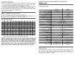
Figure 15-9. AESADIN Register

15

14

13

12

11

10

9

8

AESDIN1x (DIN Byte n+1)

w-0

w-0

w-0

w-0

w-0

w-0

w-0

w-0

7

6

5

4

3

2

1

0

AESDIN0x (DIN Byte n)

w-0

w-0

w-0

w-0

w-0

w-0

w-0

w-0

Table 15-5. AESADIN Register Description

Bit

Field

Type

Reset

Description

15-8

AESDIN1x

W

0

AES data in byte n+1 when AESADIN is written as word.

Do not use these bits for byte access.

Do not mix word and byte access.

Always reads as zero.

7-0

AESDIN0x

W

0

AES data in byte n when AESADIN is written as word.

AES next data in byte when AESADIN_L is written as byte.

Do not mix word and byte access.

Always reads as zero.

15.3.5 AESADOUT Register

AES Accelerator Data Out Register

AESADOUT is shown in

Figure 15-10

and described in

Table 15-6

.

Figure 15-10. AESADOUT Register

15

14

13

12

11

10

9

8

AESDOUT1x (DOUT Byte n+1)

r-0

r-0

r-0

r-0

r-0

r-0

r-0

r-0

7

6

5

4

3

2

1

0

AESDOUT0x (DOUT Byte n)

r-0

r-0

r-0

r-0

r-0

r-0

r-0

r-0

Table 15-6. AESADOUT Register Description

Bit

Field

Type

Reset

Description

15-8

AESDOUT1x

R

0

AES data out byte n+1 when AESADOUT is read as word.

Do not use these bits for byte access.

Do not mix word and byte access.

7-0

AESDOUT0x

R

0

AES data out byte n when AESADOUT is read as word.

AES next data out byte when AESADOUT_L is read as byte.

Do not mix word and byte access.

Summary of Contents for MSP430x5 series

Page 1: ...MSP430x5xx and MSP430x6xx Family User s Guide Literature Number SLAU208Q June 2008 Revised March 2018 ...

Page 2: ...nded Time in Low Power Modes 68 1 5 Principles for Low Power Applications 69 1 6 Connection of Unused Pins 70 1 7 Reset Pin RST NMI Configuration 70 1 8 Configuring JTAG Pins 71 1 9 Boot Code 71 1 10 Bootloader BSL 71 1 11 Memory Map Uses and Abilities 72 1 11 1 Vacant Memory Space 73 1 11 2 JTAG Lock Mechanism Using the Electronic Fuse 73 1 12 JTAG Mailbox JMB System 73 1 12 1 JMB Configuration 7...

Page 3: ...109 2 2 9 SVS and SVM Performance Modes and Wake up Times 110 2 2 10 PMM Interrupts 113 2 2 11 Port I O Control 113 2 2 12 Supply Voltage Monitor Output SVMOUT Optional 113 2 3 PMM Registers 114 2 3 1 PMMCTL0 Register 115 2 3 2 PMMCTL1 Register 116 2 3 3 SVSMHCTL Register 117 2 3 4 SVSMLCTL Register 118 2 3 5 SVSMIO Register 119 2 3 6 PMMIFG Register 120 2 3 7 PMMRIE Register 122 2 3 8 PM5CTL0 Reg...

Page 4: ...tions 162 5 2 2 Internal Very Low Power Low Frequency Oscillator VLO 162 5 2 3 Internal Trimmed Low Frequency Reference Oscillator REFO 163 5 2 4 XT1 Oscillator 163 5 2 5 XT2 Oscillator 164 5 2 6 Digitally Controlled Oscillator DCO 165 5 2 7 Frequency Locked Loop FLL 166 5 2 8 DCO Modulator 167 5 2 9 Disabling FLL Hardware and Modulator 167 5 2 10 FLL Operation From Low Power Modes 167 5 2 11 Oper...

Page 5: ... 343 7 2 Flash Memory Segmentation 344 7 2 1 Segment A 345 7 3 Flash Memory Operation 346 7 3 1 Erasing Flash Memory 346 7 3 2 Writing Flash Memory 350 7 3 3 Flash Memory Access During Write or Erase 357 7 3 4 Stopping Write or Erase Cycle 358 7 3 5 Checking Flash Memory 358 7 3 6 Configuring and Accessing the Flash Memory Controller 359 7 3 7 Flash Memory Controller Interrupts 359 7 3 8 Programmi...

Page 6: ... the DMA Controller 394 11 2 11 Using ADC10 With the DMA Controller 394 11 2 12 Using ADC12 With the DMA Controller 394 11 2 13 Using DAC12 With the DMA Controller 394 11 3 DMA Registers 395 11 3 1 DMACTL0 Register 397 11 3 2 DMACTL1 Register 398 11 3 3 DMACTL2 Register 399 11 3 4 DMACTL3 Register 400 11 3 5 DMACTL4 Register 401 11 3 6 DMAxCTL Register 402 11 3 7 DMAxSA Register 404 11 3 8 DMAxDA ...

Page 7: ...nd Bit Order 434 14 3 CRC Checksum Generation 435 14 3 1 CRC Implementation 435 14 3 2 Assembler Examples 436 14 4 CRC Registers 438 14 4 1 CRCDI Register 439 14 4 2 CRCDIRB Register 439 14 4 3 CRCINIRES Register 440 14 4 4 CRCRESR Register 440 15 AES Accelerator 441 15 1 AES Accelerator Introduction 442 15 2 AES Accelerator Operation 443 15 2 1 Encryption 444 15 2 2 Decryption 445 15 2 3 Decrypti...

Page 8: ... 1 1 Similarities and Differences From Timer_A 483 18 2 Timer_B Operation 485 18 2 1 16 Bit Timer Counter 485 18 2 2 Starting the Timer 485 18 2 3 Timer Mode Control 486 18 2 4 Capture Compare Blocks 489 18 2 5 Output Unit 492 18 2 6 Timer_B Interrupts 496 18 3 Timer_B Registers 498 18 3 1 TBxCTL Register 499 18 3 2 TBxR Register 501 18 3 3 TBxCCTLn Register 502 18 3 4 TBxCCRn Register 504 18 3 5 ...

Page 9: ...6 20 3 2 TECxCTL1 Register 558 20 3 3 TECxCTL2 Register 560 20 3 4 TECxSTA Register 561 20 3 5 TECxINT Register 562 20 3 6 TECxIV Register 563 21 Real Time Clock RTC Overview 564 21 1 RTC Overview 564 22 Real Time Clock RTC_A 565 22 1 RTC_A Introduction 566 22 2 RTC_A Operation 568 22 2 1 Counter Mode 568 22 2 2 Calendar Mode 568 22 2 3 Real Time Clock Interrupts 570 22 2 4 Real Time Clock Calibra...

Page 10: ...Register 593 22 3 35 RTCIV Register 593 23 Real Time Clock B RTC_B 594 23 1 Real Time Clock RTC_B Introduction 595 23 2 RTC_B Operation 597 23 2 1 Real Time Clock and Prescale Dividers 597 23 2 2 Real Time Clock Alarm Function 597 23 2 3 Reading or Writing Real Time Clock Registers 598 23 2 4 Real Time Clock Interrupts 598 23 2 5 Real Time Clock Calibration 600 23 2 6 Real Time Clock Operation in ...

Page 11: ...ister 643 24 4 3 RTCCTL1 Register 644 24 4 4 RTCCTL3 Register 645 24 4 5 RTCOCAL Register 645 24 4 6 RTCTCMP Register 646 24 4 7 RTCNT1 Register 647 24 4 8 RTCNT2 Register 647 24 4 9 RTCNT3 Register 647 24 4 10 RTCNT4 Register 647 24 4 11 RTCSEC Register Calendar Mode With Hexadecimal Format 648 24 4 12 RTCSEC Register Calendar Mode With BCD Format 648 24 4 13 RTCMIN Register Calendar Mode With He...

Page 12: ...egister Hexadecimal Format 669 24 4 49 RTCYEARBAKx Register BCD Format 669 24 4 50 RTCTCCTL0 Register 670 24 4 51 RTCTCCTL1 Register 670 24 4 52 RTCCAPxCTL Register 671 25 32 Bit Hardware Multiplier MPY32 672 25 1 32 Bit Hardware Multiplier MPY32 Introduction 673 25 2 MPY32 Operation 675 25 2 1 Operand Registers 676 25 2 2 Result Registers 677 25 2 3 Software Examples 678 25 2 4 Fractional Numbers...

Page 13: ...C12_A 730 28 1 ADC12_A Introduction 731 28 2 ADC12_A Operation 734 28 2 1 12 Bit ADC Core 734 28 2 2 ADC12_A Inputs and Multiplexer 734 28 2 3 Voltage Reference Generator 735 28 2 4 Auto Power Down 736 28 2 5 Sample and Conversion Timing 736 28 2 6 Conversion Memory 738 28 2 7 ADC12_A Conversion Modes 738 28 2 8 Using the Integrated Temperature Sensor 744 28 2 9 ADC12_A Grounding and Noise Conside...

Page 14: ...16 Operation 798 30 2 1 Principle of Operation 798 30 2 2 ADC Core 798 30 2 3 Voltage Reference 799 30 2 4 CTSD16 Clock 799 30 2 5 Automatic Power Down 799 30 2 6 Analog Inputs 800 30 2 7 Digital Filter 801 30 2 8 Conversion Memory Registers CTSD16MEMx 804 30 2 9 Conversion Modes 805 30 2 10 Conversion Operation Using Preload 807 30 2 11 Using the Integrated Temperature Sensor 808 30 2 12 Using th...

Page 15: ...ary Format Right Justified 839 31 4 10 DAC12_xDAT Register Twos Complement 8 Bit Binary Format Left Justified 839 31 4 11 DAC12_xCALCTL Register 840 31 4 12 DAC12_xCALDAT Register 840 31 4 13 DAC12IV Register 841 32 Comparator B Comp_B 842 32 1 Comp_B Introduction 843 32 2 Comp_B Operation 844 32 2 1 Comparator 844 32 2 2 Analog Input Switches 844 32 2 3 Port Logic 844 32 2 4 Input Short Switch 84...

Page 16: ... 34 3 7 LCDBPCTL1 Register 898 34 3 8 LCDBPCTL2 Register 899 34 3 9 LCDBPCTL3 Register 899 34 3 10 LCDBCPCTL Register 900 34 3 11 LCDBIV Register 901 35 LCD_C Controller 902 35 1 LCD_C Introduction 903 35 2 LCD_C Operation 905 35 2 1 LCD Memory 905 35 2 2 LCD Timing Generation 906 35 2 3 Blanking the LCD 907 35 2 4 LCD Blinking 907 35 2 5 LCD Voltage And Bias Generation 908 35 2 6 LCD Outputs 911 ...

Page 17: ...de 955 36 3 16 DMA Operation 956 36 4 USCI_A UART Mode Registers 957 36 4 1 UCAxCTL0 Register 958 36 4 2 UCAxCTL1 Register 959 36 4 3 UCAxBR0 Register 960 36 4 4 UCAxBR1 Register 960 36 4 5 UCAxMCTL Register 960 36 4 6 UCAxSTAT Register 961 36 4 7 UCAxRXBUF Register 962 36 4 8 UCAxTXBUF Register 962 36 4 9 UCAxIRTCTL Register 963 36 4 10 UCAxIRRCTL Register 963 36 4 11 UCAxABCTL Register 964 36 4 ...

Page 18: ... 3 I2 C Addressing Modes 999 38 3 4 I2 C Module Operating Modes 1000 38 3 5 I2 C Clock Generation and Synchronization 1011 38 3 6 Using the USCI Module in I2 C Mode With Low Power Modes 1012 38 3 7 USCI Interrupts in I2 C Mode 1012 38 4 USCI_B I2C Mode Registers 1015 38 4 1 UCBxCTL0 Register 1016 38 4 2 UCBxCTL1 Register 1017 38 4 3 UCBxBR0 Register 1018 38 4 4 UCBxBR1 Register 1018 38 4 5 UCBxSTA...

Page 19: ...gister 1054 40 Enhanced Universal Serial Communication Interface eUSCI SPI Mode 1055 40 1 Enhanced Universal Serial Communication Interfaces eUSCI_A eUSCI_B Overview 1056 40 2 eUSCI Introduction SPI Mode 1056 40 3 eUSCI Operation SPI Mode 1058 40 3 1 eUSCI Initialization and Reset 1058 40 3 2 Character Format 1059 40 3 3 Master Mode 1059 40 3 4 Slave Mode 1060 40 3 5 SPI Enable 1061 40 3 6 Serial ...

Page 20: ...107 41 4 4 UCBxSTATW 1107 41 4 5 UCBxTBCNT Register 1108 41 4 6 UCBxRXBUF Register 1109 41 4 7 UCBxTXBUF 1109 41 4 8 UCBxI2COA0 Register 1110 41 4 9 UCBxI2COA1 Register 1111 41 4 10 UCBxI2COA2 Register 1111 41 4 11 UCBxI2COA3 Register 1112 41 4 12 UCBxADDRX Register 1112 41 4 13 UCBxADDMASK Register 1113 41 4 14 UCBxI2CSA Register 1113 41 4 15 UCBxIE Register 1114 41 4 16 UCBxIFG Register 1116 41 ...

Page 21: ... 43 2 5 Current Limitation and Overload Protection 1179 43 2 6 LDO PWR Interrupts 1180 43 2 7 Port U Control 1180 43 3 LDO PWR Registers 1181 43 3 1 LDOKEYPID Register 1182 43 3 2 PUCTL Register 1182 43 3 3 LDOPWRCTL Register 1183 44 Embedded Emulation Module EEM 1184 44 1 Embedded Emulation Module EEM Introduction 1185 44 2 EEM Building Blocks 1187 44 2 1 Triggers 1187 44 2 2 Trigger Sequencer 11...

Page 22: ...Voltage and Core Voltage See Device Specific Data Sheet 99 2 2 PMM Block Diagram 100 2 3 Available SVMH Settings Versus VCORE Settings 103 2 4 High Side and Low Side Voltage Failure and Resulting PMM Actions 104 2 5 High Side SVS and SVM 105 2 6 Low Side SVS and SVM 106 2 7 PMM Action at Device Power Up 107 2 8 Changing VCORE and SVML and SVSL Levels 108 2 9 PMMCTL0 Register 115 2 10 PMMCTL1 Regis...

Page 23: ...r 179 5 11 UCSCTL5 Register 180 5 12 UCSCTL6 Register 181 5 13 UCSCTL7 Register 183 5 14 UCSCTL8 Register 184 5 15 UCSCTL9 Register 185 6 1 MSP430X CPU Block Diagram 188 6 2 PC Storage on the Stack for Interrupts 189 6 3 Program Counter 190 6 4 PC Storage on the Stack for CALLA 190 6 5 Stack Pointer 191 6 6 Stack Usage 191 6 7 PUSHX A Format on the Stack 191 6 8 PUSH SP POP SP Sequence 191 6 9 SR ...

Page 24: ...r 280 6 44 Rotate Left Arithmetically RLAM W and RLAM A 307 6 45 Destination Operand Arithmetic Shift Left 308 6 46 Destination Operand Carry Left Shift 309 6 47 Rotate Right Arithmetically RRAM W and RRAM A 310 6 48 Rotate Right Arithmetically RRAX B A Register Mode 312 6 49 Rotate Right Arithmetically RRAX B A Non Register Mode 312 6 50 Rotate Right Through Carry RRCM W and RRCM A 314 6 51 Rotat...

Page 25: ...11 7 DMACTL1 Register 398 11 8 DMACTL2 Register 399 11 9 DMACTL3 Register 400 11 10 DMACTL4 Register 401 11 11 DMAxCTL Register 402 11 12 DMAxSA Register 404 11 13 DMAxDA Register 405 11 14 DMAxSZ Register 406 11 15 DMAIV Register 407 12 1 P1IV Register 422 12 2 P2IV Register 423 12 3 P1IES Register 424 12 4 P1IE Register 424 12 5 P1IFG Register 424 12 6 P2IES Register 425 12 7 P2IE Register 425 1...

Page 26: ...ode Flag Setting 466 17 9 Output Unit in Up Down Mode 467 17 10 Capture Signal SCS 1 468 17 11 Capture Cycle 468 17 12 Output Example Timer in Up Mode 470 17 13 Output Example Timer in Continuous Mode 471 17 14 Output Example Timer in Up Down Mode 472 17 15 Capture Compare Interrupt Flag 473 17 16 TAxCTL Register 476 17 17 TAxR Register 477 17 18 TAxCCTLn Register 478 17 19 TAxCCRn Register 480 17...

Page 27: ...ode 523 19 17 COV in Dual Capture Mode 523 19 18 Output Example Channel 1 Timer in Up Mode 527 19 19 Output Example Channel 1 Timer in Up Mode With External Fault Signal 528 19 20 Output Example Timer in Up Mode with External Timer Clear Signal 529 19 21 Output Example Timer in Continuous Mode 530 19 22 Output Example Timer in Up Down Mode 531 19 23 Capture Compare TDxCCR0 Interrupt Flag 532 19 24...

Page 28: ...AY Register 583 22 19 RTCMON Register 584 22 20 RTCMON Register 584 22 21 RTCYEARL Register 585 22 22 RTCYEARL Register 585 22 23 RTCYEARH Register 586 22 24 RTCYEARH Register 586 22 25 RTCAMIN Register 587 22 26 RTCAMIN Register 587 22 27 RTCAHOUR Register 588 22 28 RTCAHOUR Register 588 22 29 RTCADOW Register 589 22 30 RTCADAY Register 589 22 31 RTCADAY Register 590 22 32 RTCPS0CTL Register 591 ...

Page 29: ...ister 621 24 1 RTC_C Block Diagram RTCMODE 1 624 24 2 RTC_C Offset Error Calibration and Temperature Compensation Scheme 631 24 3 RTC_C Functional Block Diagram in Counter Mode RTCMODE 0 634 24 4 RTCCTL0_L Register 642 24 5 RTCCTL0_H Register 643 24 6 RTCCTL1 Register 644 24 7 RTCCTL3 Register 645 24 8 RTCOCAL Register 645 24 9 RTCTCMP Register 646 24 10 RTCNT1 Register 647 24 11 RTCNT2 Register 6...

Page 30: ...CYEARBAKx Register 669 24 52 RTCYEARBAKx Register 669 24 53 RTCTCCTL0 Register 670 24 54 RTCTCCTL1 Register 670 24 55 RTCCAPxCTL Register 671 25 1 MPY32 Block Diagram 674 25 2 Q15 Format Representation 679 25 3 Q14 Format Representation 679 25 4 Saturation Flow Chart 681 25 5 Multiplication Flow Chart 683 25 6 MPY32CTL0 Register 689 26 1 REF Block Diagram 692 26 2 REF Block Diagram for Devices Wit...

Page 31: ...rations 745 28 13 ADC12CTL0 Register 750 28 14 ADC12CTL1 Register 752 28 15 ADC12CTL2 Register 753 28 16 ADC12MEMx Register 754 28 17 ADC12MCTLx Register 755 28 18 ADC12IE Register 756 28 19 ADC12IFG Register 758 28 20 ADC12IV Register 760 29 1 SD24_B Overview Block Diagram 763 29 2 SD24_B Reference and Clock Generation Block Diagram 764 29 3 SD24_B Converter Block Diagram 765 29 4 Sigma Delta Pri...

Page 32: ...ion Using Preload Example 807 30 12 Preload and Channel Synchronization 808 30 13 Typical Temperature Sensor Transfer Function 808 30 14 CTSD16CTL Register 812 30 15 CTSD16CCTL0 to CTSD16CCTL6 Register 813 30 16 CTSD16MEM0 to CTSD16MEM6 Register 814 30 17 CTSD16INCTL0 to CTSD16INCTL6 Register 815 30 18 CTSD16PRE0 to CTSD16PRE6 Register 816 30 19 CTSD16IFG Register 817 30 20 CTSD16IE Register 819 3...

Page 33: ... Segments Maximum 871 34 3 Bias Generation 874 34 4 Example Static Waveforms 877 34 5 Static LCD Example MAB addresses need to be replaced with LCDMx 878 34 6 Example 2 Mux Waveforms 880 34 7 2 Mux LCD Example MAB addresses need to be replaced with LCDMx 881 34 8 Example 3 Mux Waveforms 883 34 9 3 Mux LCD Example MAB addresses need to be replaced with LCDMx 884 34 10 Example 4 Mux Waveforms 886 34...

Page 34: ...42 36 5 Auto Baud Rate Detection Break Synch Sequence 943 36 6 Auto Baud Rate Detection Synch Field 943 36 7 UART vs IrDA Data Format 945 36 8 Glitch Suppression USCI Receive Not Started 947 36 9 Glitch Suppression USCI Activated 947 36 10 BITCLK Baud Rate Timing With UCOS16 0 948 36 11 Receive Error 951 36 12 UCAxCTL0 Register 958 36 13 UCAxCTL1 Register 959 36 14 UCAxBR0 Register 960 36 15 UCAxB...

Page 35: ...C Module 10 Bit Addressing Format 999 38 7 I2 C Module Addressing Format With Repeated START Condition 999 38 8 I2 C Time Line Legend 1000 38 9 I2 C Slave Transmitter Mode 1001 38 10 I2 C Slave Receiver Mode 1003 38 11 I2 C Slave 10 Bit Addressing Mode 1004 38 12 I2 C Master Transmitter Mode 1006 38 13 I2 C Master Receiver Mode 1008 38 14 I2 C Master 10 Bit Addressing Mode 1009 38 15 Arbitration P...

Page 36: ...k Diagram SPI Mode 1057 40 2 eUSCI Master and External Slave UCSTEM 0 1059 40 3 eUSCI Slave and External Master 1060 40 4 eUSCI SPI Timing With UCMSB 1 1062 40 5 UCAxCTLW0 Register 1065 40 6 UCAxBRW Register 1066 40 7 UCAxSTATW Register 1067 40 8 UCAxRXBUF Register 1068 40 9 UCAxTXBUF Register 1069 40 10 UCAxIE Register 1070 40 11 UCAxIFG Register 1071 40 12 UCAxIV Register 1072 40 13 UCBxCTLW0 Re...

Page 37: ...UCBxADDRX Register 1112 41 29 UCBxADDMASK Register 1113 41 30 UCBxI2CSA Register 1113 41 31 UCBxIE Register 1114 41 32 UCBxIFG Register 1116 41 33 UCBxIV Register 1118 42 1 USB Block Diagram 1121 42 2 USB Power System 1123 42 3 USB Power Up and Down Profile 1124 42 4 Powering Entire MSP430 From VBUS 1125 42 5 USB PLL Analog Block Diagram 1126 42 6 Data Buffers and Descriptors 1129 42 7 USB Timer a...

Page 38: ...Register 1170 42 34 USBOEPBBAY_n Register 1170 42 35 USBOEPBCTY_n Register 1171 42 36 USBOEPSIZXY_n Register 1171 42 37 USBIEPCNF_n Register 1172 42 38 USBIEPBBAX_n Register 1173 42 39 USBIEPBCTX_n Register 1174 42 40 USBIEPBBAY_n Register 1174 42 41 USBIEPBCTY_n Register 1175 42 42 USBIEPSIZXY_n Register 1175 43 1 LDO Block Diagram 1177 43 2 3 3 V LDO Power Up Down Profile 1178 43 3 Powering Enti...

Page 39: ...cription 92 1 22 SYSJMBO0 Register Description 93 1 23 SYSJMBO1 Register Description 93 1 24 SYSUNIV Register Description 94 1 25 SYSSNIV Register Description 95 1 26 SYSRSTIV Register Description 96 1 27 SYSBERRIV Register Description 97 2 1 SVS and SVM Thresholds 102 2 2 Recommended SVSL Settings 102 2 3 Recommended SVSH Settings 102 2 4 Available SVSH and SVMH Settings Versus VCORE Settings 103...

Page 40: ...ster Description 176 5 5 UCSCTL2 Register Description 177 5 6 UCSCTL3 Register Description 178 5 7 UCSCTL4 Register Description 179 5 8 UCSCTL5 Register Description 180 5 9 UCSCTL6 Register Description 181 5 10 UCSCTL7 Register Description 183 5 11 UCSCTL8 Register Description 184 5 12 UCSCTL9 Register Description 185 6 1 SR Bit Description 192 6 2 Values of Constant Generators CG1 CG2 193 6 3 Sou...

Page 41: ...iption 398 11 7 DMACTL2 Register Description 399 11 8 DMACTL3 Register Description 400 11 9 DMACTL4 Register Description 401 11 10 DMAxCTL Register Description 402 11 11 DMAxSA Register Description 404 11 12 DMAxDA Register Description 405 11 13 DMAxSZ Register Description 406 11 14 DMAIV Register Description 407 12 1 I O Configuration 410 12 2 Digital I O Registers 416 12 3 P1IV Register Descript...

Page 42: ...tion 477 17 6 TAxCCTLn Register Description 478 17 7 TAxCCRn Register Description 480 17 8 TAxIV Register Description 480 17 9 TAxEX0 Register Description 481 18 1 Timer Modes 486 18 2 TBxCLn Load Events 491 18 3 Compare Latch Operating Modes 492 18 4 Output Modes 492 18 5 Timer_B Registers 498 18 6 TBxCTL Register Description 499 18 7 TBxR Register Description 501 18 8 TBxCCTLn Register Descripti...

Page 43: ...ription 579 22 8 RTCNT3 Register Description 579 22 9 RTCNT4 Register Description 579 22 10 RTCSEC Register Description 580 22 11 RTCSEC Register Description 580 22 12 RTCMIN Register Description 581 22 13 RTCMIN Register Description 581 22 14 RTCHOUR Register Description 582 22 15 RTCHOUR Register Description 582 22 16 RTCDOW Register Description 583 22 17 RTCDAY Register Description 583 22 18 RT...

Page 44: ...ster Description 613 23 21 RTCAHOUR Register Description 614 23 22 RTCAHOUR Register Description 614 23 23 RTCADOW Register Description 615 23 24 RTCADAY Register Description 616 23 25 RTCADAY Register Description 616 23 26 RTCPS0CTL Register Description 617 23 27 RTCPS1CTL Register Description 618 23 28 RTCPS0 Register Description 619 23 29 RTCPS1 Register Description 619 23 30 RTCIV Register Des...

Page 45: ... Description 661 24 38 RTCPS1 Register Description 661 24 39 RTCIV Register Description 662 24 40 BIN2BCD Register Description 663 24 41 BCD2BIN Register Description 663 24 42 RTCSECBAKx Register Description 664 24 43 RTCSECBAKx Register Description 664 24 44 RTCMINBAKx Register Description 665 24 45 RTCMINBAKx Register Description 665 24 46 RTCHOURBAKx Register Description 666 24 47 RTCHOURBAKx R...

Page 46: ...on 727 27 14 ADC10IFG Register Description 728 27 15 ADC10IV Register Description 729 28 1 ADC12_A Conversion Result Formats 738 28 2 Conversion Mode Summary 738 28 3 ADC12_A Registers 748 28 4 ADC12CTL0 Register Description 750 28 5 ADC12CTL1 Register Description 752 28 6 ADC12CTL2 Register Description 753 28 7 ADC12MEMx Register Description 754 28 8 ADC12MCTLx Register Description 755 28 9 ADC12...

Page 47: ...DAC12_xCTL0 Register Description 833 31 6 DAC12_xCTL1 Register Description 835 31 7 DAC12_xDAT Register Description 836 31 8 DAC12_xDAT Register Description 836 31 9 DAC12_xDAT Register Description 837 31 10 DAC12_xDAT Register Description 837 31 11 DAC12_xDAT Register Description 838 31 12 DAC12_xDAT Register Description 838 31 13 DAC12_xDAT Register Description 839 31 14 DAC12_xDAT Register Desc...

Page 48: ...CTL Register Description 929 35 11 LCDCMEMCTL Register Description 930 35 12 LCDCVCTL Register Description 931 35 13 LCDCPCTL0 Register Description 933 35 14 LCDCPCTL1 Register Description 933 35 15 LCDCPCTL2 Register Description 934 35 16 LCDCPCTL3 Register Description 934 35 17 LCDCCPCTL Register Description 935 35 18 LCDCIV Register Description 935 36 1 Receive Error Conditions 946 36 2 BITCLK ...

Page 49: ...n 990 37 23 UCBxIE Register Description 991 37 24 UCBxIFG Register Description 991 37 25 UCBxIV Register Description 992 38 1 I2 C State Change Interrupt Flags 1013 38 2 USCI_B Registers 1015 38 3 UCBxCTL0 Register Description 1016 38 4 UCBxCTL1 Register Description 1017 38 5 UCBxBR0 Register Description 1018 38 6 UCBxBR1 Register Description 1018 38 7 UCBxSTAT Register Description 1019 38 8 UCBxR...

Page 50: ...CBxSTATW Register Description 1075 40 15 UCBxRXBUF Register Description 1076 40 16 UCBxTXBUF Register Description 1076 40 17 UCBxIE Register Description 1077 40 18 UCBxIFG Register Description 1077 40 19 UCBxIV Register Description 1078 41 1 Glitch Filter Length Selection Bits 1095 41 2 I2 C State Change Interrupt Flags 1100 41 3 eUSCI_B Registers 1102 41 4 UCBxCTLW0 Register Description 1103 41 5...

Page 51: ...tion 1158 42 22 USBVECINT Register Description 1159 42 23 USBMAINT Register Description 1160 42 24 USBTSREG Register Description 1161 42 25 USBFN Register Description 1161 42 26 USBCTL Register Description 1162 42 27 USBIE Register Description 1163 42 28 USBIFG Register Description 1164 42 29 USBFUNADR Register Description 1164 42 30 USB Buffer Memory 1165 42 31 USB Buffer Descriptor Registers 116...

Page 52: ...isit http www ti com msp430 Notational Conventions Program examples are shown in a special typeface Glossary ACLK Auxiliary Clock see Section 5 1 ADC Analog to Digital Converter BOR Brownout Reset see Section 1 2 BSL Bootloader see www ti com msp430 for application reports CPU Central Processing Unit see Section 6 1 DAC Digital to Analog Converter DCO Digitally Controlled Oscillator see Section 5 ...

Page 53: ...S Top of stack see Section 6 3 2 UNMI User NMI see Section 1 3 1 WDT Watchdog Timer see Chapter 16 z16 16 bit address space Register Bit Conventions Each register is shown with a key indicating the accessibility of the each individual bit and the initial condition Register Bit Accessibility and Initial Condition Key Bit Accessibility rw Read write r Read only r0 Read as 0 r1 Read as 1 w Write only...

Page 54: ... SNMI and UNMI event source selection and management Address decoding A user data exchange mechanism using the JTAG mailbox JMB Bootloader BSL entry mechanism Configuration management device descriptors Provides interrupt vector generators for reset and NMIs Topic Page 1 1 System Control Module SYS Introduction 55 1 2 System Reset and Initialization 55 1 3 Interrupts 57 1 4 Operating Modes 63 1 5 ...

Page 55: ...ering up the device A low signal on RST NMI pin when configured in the reset mode A wake up event from LPMx 5 LPM3 5 or LPM4 5 modes A software BOR event A security violation access of protected areas in flash such as protected BSL A POR is always generated when a BOR is generated but a BOR is not generated by a POR The following events trigger a POR A BOR signal A SVSH and or SVSM low condition w...

Page 56: ...VLRIFG from SVML s SVMLVLRPE Delay POR WDTIFG Watchdog Timer s EN from port wakeup logic s PUC Logic Module PUCs MCLK notRST Delay clr clr clr System Reset and Initialization www ti com 56 SLAU208Q June 2008 Revised March 2018 Submit Documentation Feedback Copyright 2008 2018 Texas Instruments Incorporated System Resets Interrupts and Operating Modes System Control Module SYS Figure 1 1 BOR POR PU...

Page 57: ...ments The following must occur Initialize the stack pointer SP typically to the top of RAM Initialize the watchdog to the requirements of the application Configure peripheral modules to the requirements of the application NOTE A device that is unprogrammed or blank is defined as having its reset vector value residing at memory address FFFEh equal to FFFFh Upon system reset of a blank device the de...

Page 58: ...I interrupt is accepted other NMIs of that level are automatically disabled to prevent nesting of consecutive NMIs of the same level Program execution begins at the address stored in the NMI vector as shown in Table 1 1 To allow software backward compatibility to users of earlier MSP430 families the software may but does not need to reenable NMI sources The block diagram for NMI sources is shown i...

Page 59: ...s With Reentrance Protection 1 3 3 Maskable Interrupts Maskable interrupts are caused by peripherals with interrupt capability Each maskable interrupt source can be disabled individually by an interrupt enable bit or all maskable interrupts can be disabled by the general interrupt enable GIE bit in the status register SR Each individual peripheral interrupt is discussed in its respective module ch...

Page 60: ... is loaded into the PC the program continues with the interrupt service routine at that address Figure 1 4 Interrupt Processing NOTE Enable and Disable Interrupt Due to the pipelined CPU architecture setting the general interrupt enable GIE requires special care The instruction immediately after the enable interrupts instruction EINT is always executed even if an interrupt service request is pendi...

Page 61: ...ring during an interrupt service routine interrupts the routine regardless of the interrupt priorities 1 3 6 Interrupt Vectors The interrupt vectors are located in the address range 0FFFFh to 0FF80h for a maximum of 64 interrupt sources A vector is programmed by the user and points to the start location of the corresponding interrupt service routine Table 1 1 is an example of the interrupt vectors...

Page 62: ...ffect the SYSRSTIV SYSSNIV SYSUNIV values Reading SYSRSTIV SYSSNIV SYSUNIV register automatically resets the highest pending interrupt flag of that register If another interrupt flag is set another interrupt is immediately generated after servicing the initial interrupt Writing to the SYSRSTIV SYSSNIV SYSUNIV register automatically resets all pending interrupt flags of the group 1 3 7 1 SYSSNIV So...

Page 63: ...stack during an interrupt service routine Program flow returns to the previous operating mode if the saved SR value is not altered during the interrupt service routine Program flow can be returned to a different operating mode by manipulating the saved SR value on the stack inside of the interrupt service routine When setting any of the mode control bits the selected operating mode takes effect im...

Page 64: ...tional RTC VCORE CPUOFF 1 OSCOFF 0 SCG0 0 SCG1 0 CPUOFF 1 OSCOFF 0 SCG0 1 SCG1 0 CPUOFF 1 OSCOFF 0 SCG0 0 SCG1 1 CPUOFF 1 OSCOFF 0 SCG0 1 SCG1 1 CPUOFF 1 OSCOFF 1 SCG0 1 SCG1 1 PMMREGOFF 1 PMM Password violation to LPMx 5 SVMH OVP fault SVML OVP fault From active mode Events Operating modes Reset phases Arbitrary transitions Any enabled interrupt and NMI performs this transition An enabled reset a...

Page 65: ...ed 0 0 0 1 LPM0 CPU MCLK are disabled ACLK is active SMCLK optionally active SMCLKOFF 0 DCO is enabled if sources ACLK or SMCLK SMCLKOFF 0 DCO bias is enabled if DCO is enabled or DCO sources MCLK or SMCLK SMCLKOFF 0 FLL is enabled if DCO is enabled 0 1 0 1 LPM1 CPU MCLK are disabled ACLK is active SMCLK optionally active SMCLKOFF 0 DCO is enabled if sources ACLK or SMCLK SMCLKOFF 0 DCO bias is en...

Page 66: ...operating mode The SR bits stored on the stack can be modified within the interrupt service routine returning to a different operating mode when the RETI instruction is executed Example 1 1 shows assembly code examples of entering and exiting low power modes Example 1 2 shows C code examples of entering and exiting low power modes Example 1 1 Examples of Entering and Exiting LPM in Assembly Enter ...

Page 67: ...han the other low power modes LPMx 5 when used properly gives the lowest power consumption available on a device To achieve this entry to LPMx 5 disables the LDO of the PMM module removing the supply voltage from the core of the device Since the supply voltage is removed from the core all register contents as well as SRAM contents are lost Exit from LPMx 5 causes a BOR event which forces a complet...

Page 68: ...onal care may be required Should the respective interrupt event should occur during LPMx 5 entry the device may not recognize this or any future interrupt wake up event on this function Exit from LPMx 5 is possible with a RST event a power on cycle or through specific I O Any exit from LPMx 5 causes a BOR Program execution continues at the location stored in the system reset vector location 0FFFEh...

Page 69: ... low power integrated peripheral modules in place of software driven functions For example Timer_A and Timer_B can automatically generate PWM and capture external timing with no CPU resources Calculated branching and fast table look ups should be used in place of flag polling and long software calculations Avoid frequent subroutine and function calls due to overhead For longer software routines si...

Page 70: ...SB devices only when USB module is not being used in the application Px y Open Switched to port function output direction PxDIR n 1 Px y represents port x and bit y of port x for example P1 0 P1 1 P2 2 PJ 0 PJ 1 RST NMI DVCC or VCC 47 kΩ pullup or internal pullup selected with 10 nF 2 2 nF pulldown 3 TEST Open This pin always has an internal pulldown enabled V18 Open For USB devices only when USB ...

Page 71: ...ondition is applied The BSL enables the user to communicate with the embedded memory in the microcontroller during the prototyping phase final production and in service All memory mapped resources the programmable memory flash memory the data memory RAM and the peripherals can be modified by the BSL as required The user can define custom BSL code for flash based devices and protect it against eras...

Page 72: ...s Protectable for read write accesses Always able to access PMM registers from 1 Mass erase by user possible Mass erase by user possible Bank erase by user possible Segment erase by user possible Address Range Name and Usage Properties 00000h 00FFFh Peripherals with gaps 00000h 000FFh Reserved for system extension 00100h 00FEFh Peripherals x 00FF0h 00FF3h Descriptor type 2 x 00FF4h 00FF7h Start ad...

Page 73: ... the JTAG Interface User s Guide SLAU320 Some JTAG commands are still possible after the device is secured including the BYPASS command see IEEE1149 2001 Standard and the JMB_EXCHANGE command which allows access to the JTAG Mailbox System see Section 1 12 for details NOTE If a device has been protected TI cannot access the device for a customer return Access is only possible if a BSL is provided w...

Page 74: ...has been read by the JTAG port and are ready to receive data If JMBOUTIE is set these events cause a system NMI In 16 bit mode JMBOUTIFG is cleared automatically when data is written to JMBOUT0 In 32 bit mode JMBOUTIFG Is cleared automatically when data is written to both JMBOUT0 and JMBOUT1 In addition the JMBOUTIFG can be cleared when reading SYSSNIV Clearing JMBOUTIE disables the NMI interrupt ...

Page 75: ...other value than 80h read at address location 00FF0h indicates the device is of an older family and contains a flat descriptor beginning at location 0FF0h The information block shown in Figure 1 7 contains the device ID die revisions firmware revisions and other manufacturer and tool related information The descriptors contains information about the available peripherals their subtypes and address...

Page 76: ...EXT FEh Tag extender Each tag field is unique to its respective descriptor and is always followed by a length field The length field is one byte if the tag value is 01h through 0FDh and represents the length of the descriptor in bytes If the tag value equals 0FEh TAGEXT the next byte extends the tag values and the following two bytes represent the length of the descriptor in bytes In this way a us...

Page 77: ... section in the device specific data sheet for the availability and details on Peripheral Discovery Descriptor Table 1 5 Peripheral Discovery Descriptor Element Size bytes Comments Memory entry 1 2 Optional Memory entry 2 2 Optional 2 Optional Delimiter 00h 1 Mandatory Peripheral count 1 Mandatory Peripheral entry 1 2 Optional Peripheral entry 2 2 Optional 2 Optional Interrupt priority N 3 1 Optio...

Page 78: ...10 256 B 0000010 011 Reserved 0011 512 B 0000011 100 FLASH 0100 1KB 0000100 101 ROM 0101 2KB 0000101 110 MemType appended 0110 4KB 0000110 111 Undefined 0111 8KB 0000111 1000 16KB 0001000 1001 32KB 0001001 1010 64KB 0001010 1011 128KB 0001011 1100 256KB 0001100 1101 512KB 1110 Size appended 1111 Undefined 1111111 1 The Peripheral IDs are listed in Table 1 8 This is not a complete list but shown as...

Page 79: ...1 This table is not a complete list of all peripheral IDs that might be available on a device and is shown here for illustrative purposes only Table 1 8 Peripheral IDs 1 Peripheral or Module PID No Module 00h WDT 01h SFR 02h UCS 03h SYS 04h PMM 05h Flash Controller 08h CRC16 09h Port 1 2 51h Port 3 4 52h Port 5 6 53h Port 7 8 54h Port 9 10 55h Port J 5Fh Timer A0 81h Timer A1 82h Special info appe...

Page 80: ...L at address 0140h 0130h 10h 09h 01h 00001001_0_0000001 peripheral CRC16 at address 0150h 0140h 10h 04h 01h 00000100_0_0000001 peripheral SYS at address 0160h 0150h 10h 51h 0Ah 01010001_0_0001010 peripheral Port 1 2 at address 0200h 0160h 10h 10h 52h 02h 01010010_0_0000010 peripheral Port 3 4 at address 0220h 0200h 02h 10h 53h 02h 01010011_0_0000010 peripheral Port 5 6 at address 0240h 0220h 02h 1...

Page 81: ...0x1A04 through 0x1AFF The CRC checksum can be easily computed using the CRC16 module The following simplified C code utilizes the CRC16 module to compute the checksum See the CRC16 chapter for further details on the CRC algorithm implementation NOTE The CRC module on the MSP430F543x and MSP430F541x non A versions does not support the bit wise reverse feature used in this code example Registers CRC...

Page 82: ... The measured values are normalized by 1 5 V 2 0 V or 2 5 V before being stored into the TLV structure 2 In this way a conversion result is corrected by multiplying it with the CAL_15VREF_FACTOR or CAL_20VREF_FACTOR CAL_25VREF_FACTOR and dividing the result by 215 as shown for each of the respective reference voltages 3 In the following example the integrated 1 5 V reference voltage is used during...

Page 83: ...temperatures 30 C 3 C and 85 C 3 C and are stored in the TLV structure The characteristic equation of the temperature sensor voltage in mV is 8 The temperature coefficient TCSENSORin mV C represents the slope of the equation VSENSOR in mV represents the y intercept of the equation Temp in C is the temperature of interest The temperature Temp C can be computed as follows for each of the reference v...

Page 84: ...te register access For a generic register ANYREG the suffix _L ANYREG_L refers to the lower byte of the register bits 0 through 7 The suffix _H ANYREG_H refers to the upper byte of the register bits 8 through 15 Table 1 10 SFR Base Address Module Base Address SFR 00100h Table 1 11 SFR Registers Offset Acronym Register Name Type Access Reset Section 00h SFRIE1 Interrupt Enable Read write Word 0000h...

Page 85: ...errupts disabled 1b Interrupts enabled 6 JMBINIE RW 0h JTAG mailbox input interrupt enable flag 0b Interrupts disabled 1b Interrupts enabled 5 ACCVIE RW 0h Flash controller access violation interrupt enable flag 0b Interrupts disabled 1b Interrupts enabled 4 NMIIE RW 0h NMI pin interrupt enable flag 0b Interrupts disabled 1b Interrupts enabled 3 VMAIE RW 0h Vacant memory access interrupt enable fl...

Page 86: ...received by the JTAG module and are ready for new messages from the CPU 6 JMBINIFG RW 0h JTAG mailbox input interrupt flag 0b No interrupt pending When in 16 bit mode JMBMODE 0 this bit is cleared automatically when JMBI0 is read by the CPU When in 32 bit mode JMBMODE 1 this bit is cleared automatically when both JMBI0 and JMBI1 have been read by the CPU This bit is also cleared when the associate...

Page 87: ...0 Table 1 14 SFRRPCR Register Description Bit Field Type Reset Description 15 4 Reserved R 0h Reserved Always reads as 0 3 SYSRSTRE RW 1h Reset pin resistor enable 0b Pullup pulldown resistor at the RST NMI pin is disabled 1b Pullup pulldown resistor at the RST NMI pin is enabled 2 SYSRSTUP RW 1h Reset resistor pin pullup pulldown 0b Pulldown is selected 1b Pullup is selected 1 SYSNMIIES RW 0h NMI...

Page 88: ...L_L Read write Byte 00h 01h SYSCTL_H Read write Byte 00h 02h SYSBSLC Bootloader Configuration Read write Word 0003h Section 1 15 2 02h SYSBSLC_L Read write Byte 03h 03h SYSBSLC_H Read write Byte 00h 06h SYSJMBC JTAG Mailbox Control Read write Word 0000h Section 1 15 3 06h SYSJMBC_L Read write Byte 00h 07h SYSJMBC_H Read write Byte 00h 08h SYSJMBI0 JTAG Mailbox Input 0 Read write Word 0000h Section...

Page 89: ...nently enables the JTAG function This bit can be set only once After it is set it remains set until a BOR occurs 0b Shared JTAG pins JTAG mode selectable by SBW sequence 1b Dedicated JTAG pins explicit 4 wire JTAG mode selection 4 SYSBSLIND RW 0h BSL entry indication This bit indicates a BSL entry sequence detected on the Spy Bi Wire pins 0b No BSL entry sequence detected 1b BSL entry sequence det...

Page 90: ...owever the boot code that checks for an available BSL may set this bit by software to protect the BSL Because devices normally come with a TI BSL preprogrammed and protected the boot code sets this bit 0b Area not protected Read program and erase of BSL memory is possible 1b Area protected 14 SYSBSLOFF RW 0h BSL memory disable for the size covered in SYSBSLSIZE 0b BSL memory is addressed when this...

Page 91: ... bit transfers using JMBO0 and JMBI0 only 1b 32 bit transfers using JMBI0 JMBI1 JMBO0 and JMBO1 3 JMBOUT1FG RW 1h Outgoing JTAG Mailbox 1 flag This bit is cleared automatically when a message is written to the upper byte of JMBO1 or as word access by the CPU DMA and is set after the message was read by JTAG 0b JMBO1 is not ready to receive new data 1b JMBO1 is ready to receive new data 2 JMBOUT0FG...

Page 92: ...0 r 0 r 0 r 0 r 0 r 0 r 0 Table 1 20 SYSJMBI0 Register Description Bit Field Type Reset Description 15 8 MSGHI R 0h JTAG mailbox incoming message high byte 7 0 MSGLO R 0h JTAG mailbox incoming message low byte 1 15 5 SYSJMBI1 Register JTAG Mailbox Input 0 Register Figure 1 15 SYSJMBI1 Register 15 14 13 12 11 10 9 8 MSGHI r 0 r 0 r 0 r 0 r 0 r 0 r 0 r 0 7 6 5 4 3 2 1 0 MSGLO r 0 r 0 r 0 r 0 r 0 r 0...

Page 93: ...w 0 rw 0 rw 0 rw 0 rw 0 Table 1 22 SYSJMBO0 Register Description Bit Field Type Reset Description 15 8 MSGHI RW 0h JTAG mailbox outgoing message high byte 7 0 MSGLO RW 0h JTAG mailbox outgoing message low byte 1 15 7 SYSJMBO1 Register JTAG Mailbox Output 1 Register Figure 1 17 SYSJMBO1 Register 15 14 13 12 11 10 9 8 MSGHI rw 0 rw 0 rw 0 rw 0 rw 0 rw 0 rw 0 rw 0 7 6 5 4 3 2 1 0 MSGL0 rw 0 rw 0 rw 0...

Page 94: ... corresponding include file of the device in use Figure 1 18 SYSUNIV Register 15 14 13 12 11 10 9 8 SYSUNVEC r0 r0 r0 r0 r0 r0 r0 r0 7 6 5 4 3 2 1 0 SYSUNVEC r0 r0 r0 r 0 r 0 r 0 r 0 r0 Table 1 24 SYSUNIV Register Description Bit Field Type Reset Description 15 0 SYSUNIV R 0h User NMI vector Generates a value that can be used as address offset for fast interrupt service routine handling Writing to...

Page 95: ...NIV Register 15 14 13 12 11 10 9 8 SYSSNVEC r0 r0 r0 r0 r0 r0 r0 r0 7 6 5 4 3 2 1 0 SYSSNVEC r0 r0 r0 r 0 r 0 r 0 r 0 r0 Table 1 25 SYSSNIV Register Description Bit Field Type Reset Description 15 0 SYSSNIV R 0h System NMI vector Generates a value that can be used as address offset for fast interrupt service routine handling Writing to this register clears all pending system NMI flags 00h No inter...

Page 96: ...6 5 4 3 2 1 0 SYSRSTVEC r0 r0 r 1 r 1 r 1 r 1 r 1 r0 1 Reset value depends on reset source Table 1 26 SYSRSTIV Register Description Bit Field Type Reset Description 15 0 SYSRSTIV R 02h 3Eh 1 Reset interrupt vector Generates a value that can be used as address offset for fast interrupt service routine handling to identify the last cause of a reset BOR POR PUC Writing to this register clears all pen...

Page 97: ... include file of the used device Figure 1 21 SYSBERRIV Register 15 14 13 12 11 10 9 8 SYSBERRIV r0 r0 r0 r0 r0 r0 r0 r0 7 6 5 4 3 2 1 0 SYSBERRIV r0 r0 r0 r 0 r 0 r 0 r 0 r0 Table 1 27 SYSBERRIV Register Description Bit Field Type Reset Description 15 0 SYSBERRIV R 0h System bus error interrupt vector Generates a value that can be used as an address offset for fast interrupt service routine handli...

Page 98: ...ule and Supply Voltage Supervisor Chapter 2 SLAU208Q June 2008 Revised March 2018 Power Management Module and Supply Voltage Supervisor This chapter describes the operation of the Power Management Module PMM and Supply Voltage Supervisor SVS Topic Page 2 1 Power Management Module PMM Introduction 99 2 2 PMM Operation 101 2 3 PMM Registers 114 ...

Page 99: ...e supervision and monitoring of both the voltage applied to the device DVCC and the voltage generated for the core VCORE The PMM uses an integrated low dropout voltage regulator LDO to produce a secondary core voltage VCORE from the primary one applied to the device DVCC In general VCORE supplies the CPU memories flash and RAM and the digital modules while DVCC supplies the I Os and all analog mod...

Page 100: ...high side monitor SVMH respectively VCORE is supervised and monitored by the low side supervisor SVSL and low side monitor SVML respectively Thus there are four separate supervision and monitoring modules that can be active at any given time The thresholds enforced by these modules are derived from the same voltage reference used by the regulator to generate VCORE In addition to the SVSH SVMH SVSL...

Page 101: ... to raise VCORE for higher MCLK frequencies The regulator supports two different load settings to optimize power The high current mode is required when The CPU is in active LPM0 or LPM1 modes A clock source greater than 32 kHz is used to drive any module An interrupt is executed Otherwise the low current mode is used The hardware controls the load settings automatically according to the criteria a...

Page 102: ...ult an SVSL event always generates a POR SVSLPE 1 and TI recommends always setting SVSLPE 1 for reliable device startup Table 2 2 lists the most commonly used and recommended settings Table 2 2 Recommended SVSL Settings PMMCOREV 1 0 DVCC V SVSLRVL 1 0 Sets SVSL_IT Level SVSMLRRL 2 0 Sets SVSL_IT and SVML levels 00 1 8 00 000 01 2 0 01 001 10 2 2 10 010 11 2 4 11 011 2 2 2 1 2 Recommended SVSH Sett...

Page 103: ... PMMCOREV 1 0 SVSHRVL 1 0 Sets SVSH_IT Level SVSMHRRL 2 0 Sets SVSH_IT and SVMH Levels 00 00 through 11 000 through 011 01 00 through 11 001 through 100 10 00 through 11 010 through 101 11 00 through 11 011 through 111 Figure 2 3 Available SVMH Settings Versus VCORE Settings The behavior of the SVS and SVM according to these thresholds is best portrayed graphically Figure 2 4 shows how the supervi...

Page 104: ...SVSLIFG Set SVMHVLRIFG Set SVMLVLRIFG PMM Operation www ti com 104 SLAU208Q June 2008 Revised March 2018 Submit Documentation Feedback Copyright 2008 2018 Texas Instruments Incorporated Power Management Module and Supply Voltage Supervisor Figure 2 4 High Side and Low Side Voltage Failure and Resulting PMM Actions ...

Page 105: ... is immediately set again by hardware If the SVMHIE SVMH interrupt enable bit is set when SVMHIFG gets set an interrupt is generated If a POR is desired when SVMHIFG is set the SVMH can be configured to do so by setting the SVMHVLRPE SVMH voltage level reached POR enable bit while SVMHOVPE bit is cleared If DVCC rises above the SVMH level the SVMHVLRIFG SVMH voltage level reached interrupt flag is...

Page 106: ...T registers 2 2 2 3 Low Side Supervisor SVSL and Low Side Monitor SVML The SVSL and SVML modules are enabled by default and can be disabled by clearing SVSLE and SVMLE bits respectively Figure 2 6 shows the SVSL and SVML block diagrams Figure 2 6 Low Side SVS and SVM If VCORE falls below the SVSL level SVSLIFG SVSL interrupt flag is set If VCORE remains below the SVSL level and software attempts t...

Page 107: ...s SVSMLEVM should be cleared All the interrupt flags of SVSL and SVML remain set until cleared by a BOR or by software 2 2 3 Supply Voltage Supervisor and Monitor Power up When the device is powering up the SVSH and SVSL functions are enabled by default Initially DVCC is low and therefore the PMM holds the device in POR reset When both the SVSH and SVSL levels are met the reset is released Figure ...

Page 108: ... one It indicates that the core voltage reached the level you programmed in Step 4 Step 6 Program the SVSL to the next level As a reference the following is a C code example for increasing VCORE The sample libraries provide routines for increasing and decreasing the VCORE and should be used whenever possible C Code example for increasing core voltage Note Change core voltage one level at a time vo...

Page 109: ...remain on long enough to properly settle This is handled automatically and requires no setting by the application 2 2 7 LPM3 5 and LPM4 5 LPM3 5 and LPM4 5 are additional low power modes in which the regulator of the PMM is completely disabled providing additional power savings Not all devices support all LPMx 5 modes so see the device specific data sheet Because there is no power supplied to VCOR...

Page 110: ...al layer of protection There are two ways to control the performance mode manual and automatic In manual mode the normal full performance selection is the same for every operational mode except LPMx 5 the SVS and SVM are always disabled in LPMx 5 In this case the normal or full performance selection is made with the SVSHFP SVMHFP SVSLFP or SVMLFP bit for their respective modules In automatic mode ...

Page 111: ...2 LPM3 LPM4 0 x x Off Off tWAKE UP FAST 1 0 0 Normal Off tWAKE UP SLOW 1 0 1 Full performance Off tWAKE UP FAST 1 1 0 Normal Off tWAKE UP SLOW 1 1 1 Full performance Normal tWAKE UP FAST Table 2 7 SVSL Manual Performance Modes SVSLE SVSLFP AM LPM0 LPM1 SVSL State LPM2 LPM3 LPM4 SVSL State Wake up Time LPM2 LPM3 LPM4 0 x Off Off tWAKE UP FAST 1 0 Normal Normal tWAKE UP SLOW 1 1 Full performance Ful...

Page 112: ...nce Modes SVSHE SVSHFP AM LPM0 LPM1 SVSH State LPM2 LPM3 LPM4 SVSH State 0 x Off Off 1 0 Normal Normal 1 1 Full performance Full performance Table 2 13 SVMH Automatic Performance Control SVMHE SVMHFP AM LPM0 LPM1 SVMH State LPM2 LPM3 LPM4 SVMH State 0 x Off Off 1 0 Normal Off 1 1 Full performance Normal Table 2 14 SVMH Manual Performance Modes SVMHE SVMHFP AM LPM0 LPM1 SVMH State LPM2 LPM3 LPM4 SV...

Page 113: ...have in an uncontrolled fashion during an undervoltage event During these events outputs are disabled both normal drive and the weak pullup or pulldown function If the CPU is functioning normally and then an undervoltage event occurs any pin configured as an input has its PxIN register value locked in at the point the event occurs until voltage is restored During the undervoltage event external vo...

Page 114: ...ugh 15 Table 2 15 PMM Registers Offset Acronym Register Name Type Access Reset Section 00h PMMCTL0 PMM control register 0 Read write Word 9600h Section 2 3 1 00h PMMCTL0_L Read write Byte 00h 01h PMMCTL0_H Read write Byte 96h 02h PMMCTL1 PMM control register 1 Read write Word 0000h Section 2 3 2 02h PMMCTL1_L Read write Byte 00h 03h PMMCTL1_H Read write Byte 00h 04h SVSMHCTL SVS and SVM high side ...

Page 115: ...096h When using word operations must be written with 0A5h or a PUC is generated When using byte operation writing 0A5h unlocks all PMM registers When using byte operation writing anything different than 0A5h locks all PMM registers 7 Reserved RW 0h Reserved Must always be written as 0 6 5 Reserved R 0h Reserved Always reads as 0 4 PMMREGOFF RW 0h Regulator off see the SYS chapter for details 3 PMM...

Page 116: ...er 1 Figure 2 10 PMMCTL1 Register 15 14 13 12 11 10 9 8 Reserved r 0 r 0 r 0 r 0 r 0 r 0 r 0 r 0 7 6 5 4 3 2 1 0 Reserved Reserved Reserved Reserved r 0 r 0 rw 0 rw 0 r 0 r 0 rw 0 rw 0 Table 2 17 PMMCTL1 Register Description Bit Field Type Reset Description 15 6 Reserved R 0h Reserved Always reads as 0 5 4 Reserved RW 0h Reserved Must always be written with 0 3 2 Reserved R 0h Reserved Always read...

Page 117: ...S high side enable If this bit is set the SVSH is enabled 9 8 SVSHRVL RW 0h SVS high side reset voltage level If DVCC falls short of the SVSH voltage level selected by SVSHRVL a reset is triggered if SVSHPE 1 The voltage levels are defined in the device specific data sheet Note SVSMHRRL must always be equal or larger than SVSHRVL 7 SVSMHACE RW 0h SVS and SVM high side automatic control enable If t...

Page 118: ...pecific data sheet for response times 10 SVSLE RW 1h SVS low side enable If this bit is set the SVSL is enabled 9 8 SVSLRVL RW 0h SVS low side reset voltage level If V CORE falls short of the SVSL voltage level selected by SVSLRVL a reset is triggered if SVSLPE 1 Note SVSMLRRL must always be equal to or larger than SVSLRVL 7 SVSMLACE RW 0h SVS and SVM low side automatic control enable If this bit ...

Page 119: ...OUT pin The device specific port logic has to be configured accordingly 11 SVMHOE RW 0h SVM high side output enable If this bit is set the SVMHIFG bit is output to the device SVMOUT pin The device specific port logic has to be configured accordingly 10 6 Reserved R 0h Reserved Always reads as 0 5 SVMOUTPOL RW 1h SVMOUT pin polarity If this bit is set SVMOUT is active high An error condition is sig...

Page 120: ...b Interrupt pending 12 SVSHIFG RW 0h SVS high side interrupt flag The bit is cleared by software or by reading the reset vector word 0b No interrupt pending 1b Interrupt pending 11 Reserved R 0h Reserved Always reads as 0 10 PMMPORIFG RW 0h PMM software power on reset interrupt flag This interrupt flag is set if a software POR is triggered The bit is cleared by software or by reading the reset vec...

Page 121: ... No interrupt pending 1b Interrupt pending 3 Reserved R 0h Reserved Always reads as 0 2 SVMLVLRIFG RW 0h SVM low side voltage level reached interrupt flag The bit is cleared by software or by reading the reset vector SVSLPE 1 word or by reading the interrupt vector SVSLPE 0 word 0b No interrupt pending 1b Interrupt pending 1 SVMLIFG RW 0h SVM low side interrupt flag The bit is cleared by software ...

Page 122: ... RW 1h SVS high side power on reset enable If this bit is set falling below the SVSH voltage level triggers a POR 11 10 Reserved R 0h Reserved Always reads as 0 9 SVMLVLRPE RW 0h SVM low side voltage level reached power on reset enable If this bit is set exceeding the SVML voltage level triggers a POR 8 SVSLPE RW 1h SVS low side power on reset enable If this bit is set falling below the SVSL volta...

Page 123: ...w 0 Table 2 23 PM5CTL0 Register Description Bit Field Type Reset Description 15 1 Reserved R 0h Reserved Always reads as 0 0 LOCKLPM5 RW 0h Lock I O pin configuration upon entry to or exit from LPMx 5 When power is applied to the device this bit once set can only be cleared by the user or via another power cycle Note This bit was formerly named LOCKIO and some application reports and code examples...

Page 124: ... backup system can operate a real time clock RTC_B module and retain some bytes in a backup RAM from a backup source when the primary supply fails The battery backup system also includes a simple charging circuitry to charge capacitors connected to the backup supply This chapter describes the battery backup system Topic Page 3 1 Battery Backup Introduction 125 3 2 Battery Backup Operation 125 3 3 ...

Page 125: ...s the switching between primary and secondary supply NOTE Restrictions When the lowest high side SVS level 00b is used to monitor the primary supply the temperature range is restricted to 0 C to 85 C Figure 3 1 shows an overview of the battery backup switch The secondary supply VBAT powers the backup supplied subsystem at power on if bit BAKDIS 0 in the BAKCTL register and if the primary supply dr...

Page 126: ...acitor that may be placed on VBAT to maintain charge during backup operation in the application 3 2 1 Activate Access to Backup Supplied Subsystem If the backup supplied subsystem is powered by the secondary supply VBAT the LOCKBAK bit is automatically set While LOCKBAK 1 it is impossible to access to the information stored in the backup supplied subsystem After its supply switched back to the pri...

Page 127: ...ntegrated ADC the primary and secondary supplies can be measured Select the channel of the ADC that is reserved to measure the supply voltage of the device This is usually ADC channel 12 see the respective ADC chapter and the device specific data sheet for details If BAKADC 0 VBAT measurement is disabled If BAKADC 1 the secondary supply VBAT is measured The resistive dividers are connected to the ...

Page 128: ...es the charger and all control register bits are reset to 0 If VCC is selected as charge end voltage with BACKCHVx 01b or if VCC 2 7 V with BACKCHVx 10b an attached capacitor is charged to VCC with VBAT t VCC 1 exp t RC with R being the selected charging resistor and C being the capacitor attached to pin VBAT this is not CBAK If a charge end voltage of 2 7 V is selected BACKCHVx 10b and VCC 2 7 V ...

Page 129: ...backup registers are listed in Table 3 1 The base address for the backup RAM registers can be found in the device specific data sheet The address offsets are given in Table 3 1 Table 3 1 Battery Backup Registers Offset Acronym Register Name Type LPMx 5 Backup Retention Section 00h BAKCTL Battery Backup Control Read write not retained Section 3 3 1 02h BAKCHCTL Battery Charger Control Read write no...

Page 130: ...witching enabled 1b Backup supply switching disabled Backup subsystem always powered from VCC also during LPMx 5 2 BAKADC RW 0h Battery backup supply to ADC 0b Vbat measurement disabled 1b Vbat measurement enabled 1 BAKSW RW 0h Manual switch to battery backup supply 0b Switching is automatic 1b Switch to battery backup supply 0 LOCKBAK RW 0h Lock backup subsystem Can only be written as 0 The LOCKB...

Page 131: ...EYx RW 5Ah Charger access key Always read as 05Ah Must be written as 069h together with low byte any other write disables the charger and all control register bits are reset to 0 7 6 Reserved R 0h Reserved Always reads as 0 5 4 BAKCHVx RW 0h Charger end voltage 00b Charger disabled 01b VCC 10b Approximately 2 7 V or VCC if VCC is lower than 2 7 V 11b Reserved 3 Reserved R 0h Reserved Always reads ...

Page 132: ...ly System AUX The auxiliary supply system AUX allows the device to operate from alternate supplies also called auxiliary supplies if the primary supply DVCC and AVCC fails The AUX includes simple charging circuitry to charge capacitors connected to the auxiliary supplies This chapter describes the AUX Topic Page 4 1 Auxiliary Supply System Introduction 133 4 2 Auxiliary Supply Operation 134 4 3 AU...

Page 133: ...hold based monitoring of primary and auxiliary supplies At start up automatically chooses between the primary supply DVCC AVCC and AUXVCC1 based on which one is higher voltage A separate auxiliary supply AUXVCC3 can power a backup subsystem 1 Simple charger for capacitors on AUXVCC2 and AUXVCC3 NOTE Unused auxiliary supplies Any unused auxiliary supply inputs AUXVCC1 or AUXVCC2 must be connected t...

Page 134: ...S among the DVCC AUXVCC1 and AUXVCC2 inputs VDSYS is also output on the VDSYS pin which must be connected to an external capacitor as specified in the device specific data sheet The analog modules of the device are supplied by the internal analog system voltage VASYS The AUX module switches VASYS among the AVCC AUXVCC1 and AUXVCC2 inputs VASYS is also output on the VASYS pin which must be connecte...

Page 135: ...an 100 mV After start up from any condition that causes a BOR event including connection of power or wake from LPMx 5 the AUX module is automatically locked To configure the behavior of the auxiliary supply system write AUXKEY 0xA5 in the AUXCTL0 register to enable access to the AUXCTL1 and AUXCTL2 registers see Section 4 2 2 After configuration is completed the AUX module switches between the inp...

Page 136: ...isable a supply clear AUXxOK 0 If the current supply is software controlled AUXxMD 1 and AUXxOK is changed from 1 to 0 the next available supply considering the priority defined by AUX2PRIO is used to source the system voltages When a switch from one supply to another occurs interrupts are generated as described in Section 4 2 11 The software control can be used to permanently disable a supply or ...

Page 137: ...icates a valid or good supply voltage and AUXxOK 0 indicates an invalid or bad supply voltage See Section 4 2 6 for details on the monitoring of the auxiliary supplies NOTE Interactions among SVMH VCORE and AUX Because of the relationship between supply voltage core voltage and maximum system frequency see Section 4 2 5 for considerations when setting the AUXxLVL and SVMH levels In particular note...

Page 138: ...tions from 0 to 1 unless the SVM signals that a switch is necessary 4 2 5 Interactions Among fSYS VCORE VDSYS SVMH and AUXxLVL The interactions that must be considered when setting the threshold levels in the SVM and AUX are Minimum VCORE required to support the selected system frequency fSYS Valid SVMH to support the selected VCORE Minimum VDSYS and minimum AUXxLVL required to support the selecte...

Page 139: ...com Auxiliary Supply Operation 139 SLAU208Q June 2008 Revised March 2018 Submit Documentation Feedback Copyright 2008 2018 Texas Instruments Incorporated Auxiliary Supply System AUX Figure 4 2 System Frequency vs Supply Voltage After selecting the system frequency and PMMCOREV 1 0 values the SVM threshold must be selected Figure 4 3 shows the valid values for SVMH SVSMHRRL 2 0 based on the selecte...

Page 140: ...s the information from the preceding figures and discussions Table 4 2 Minimum Voltage Thresholds for Selected fSYS fSYS max MHz Minimum PMMCOREV 1 0 Minimum SVSMHRRL 2 0 Sets SVMH Level Minimum VDSYS Minimum AUX0LVL Minimum AUX1LVL AUX2LVL 8 00 000 1 8 V 001 000 12 01 001 2 0 V 010 001 20 10 010 2 2 V 011 010 25 11 011 2 4 V 100 011 4 2 6 Auxiliary Supply Monitor Supplies that are not currently i...

Page 141: ...AUXMRx bits By default with AUXMRx 00b the supplies are monitored continuously as described above By setting AUXMRx 01b the supplies are monitored every 32 VLO clock cycles by setting AUXMRx 10b the supplies are monitored every 1024 VLO clock cycles The AUXMONIFG bit signals the completion of each monitoring cycle If an unused supply is changed from software to hardware control AUXxMD is changed f...

Page 142: ... after wakeup from LPMx 5 and before releasing LOCKAUX The supplies monitored by hardware AUXxMD 0 are considered not okay until the status is updated for the first time by the auxiliary supply monitor Only the supply that was used during LPMx 5 is considered okay unless it drops below the programmed SVM level If this behavior is unwanted the state can be set to okay by temporarily switching to so...

Page 143: ... supply voltages can be measured if the device provides an ADC The supply to be measured is selected with the AUXADCSELx bit in the AUXADCCTL register In addition the resistive load applied to the selected supply during the sampling phase of the ADC can be selected with the AUXADCRx bits This allows to perform a health check of the supplies even when not loaded by the application The ADC supply vo...

Page 144: ...plies switched interrupt AUX0SWIFG switched to DVCC interrupt AUX1SWIFG switched to AUXVCC1 interrupt AUX2SWIFG switched to AUXVCC2 interrupt AUX1DRPIFG AUXVCC1 dropped below threshold interrupt AUX2DRPIFG AUXVCC2 dropped below threshold interrupt AUXMONIFG supply monitor interrupt The AUXSWNMIFG is set after the system switched from one supply to another supply A nonmaskable interrupt request is ...

Page 145: ...outine Disabled interrupts do not affect the AUXIV value Any read access of the AUXIV register automatically resets the highest pending interrupt flag A write access to the AUXIV register automatically resets all pending interrupt flags All interrupt flags can also be cleared by software 4 2 11 2 Auxiliary Supply Nonmaskable Interrupt If AUXSWNMIFG is configured as a nonmaskable interrupt source w...

Page 146: ...Texas Instruments Incorporated Auxiliary Supply System AUX 4 2 12 Software Flow Figure 4 9 shows a sample software flow chart for the use and control of the auxiliary supply system NOTE Configuration of the auxiliary supply system is required after wakeup from LPMx 5 None of the AUX registers are retained during LPMx 5 Figure 4 9 Software Flow Chart 4 2 13 Examples of AUX Operation The following s...

Page 147: ... without glitches when switching to AUX1 and AUX2 the thresholds for these must be equal to or higher than SVSMHRRL To minimize use of the auxiliary supplies they should be set equal to SVSMHRRL Therefore set AUX1LVL AUX2LVL 5 4 2 13 3 Example 3 This example shows configuration for running at a system frequency of 8 MHz an a nominal supply voltage of 3 3 V with settings designed to minimize power ...

Page 148: ...nd AUX2LVL to 1 When switching from AUX2 to AUX1 1 Increase AUX1LVL and AUX2LVL to 1 2 Increase the SVM level by setting SVSMHRRL 1 3 Increase core voltage level by setting PMMCOREV 1 also change SVS settings 4 Increase system frequency to 12 MHz Given that the system frequency should be changed to 8 MHz when running from AUX2 settings must be changed when switching to AUX2 1 Decrease system frequ...

Page 149: ... fields in the AUXCTL0 to AUXCTL2 registers are named according to what supplies they refer to AUX0 refers to DVCC AUX1 refers to AUXVCC1 and AUX2 refers to AUXVCC2 In any description the occurence of a bit name like AUXx refers to all the bit names AUX0 AUX1 and AUX2 1 Access protected by key AUXKEY in AUXCTL0 Table 4 4 Auxiliary Supply Registers Offset Acronym Register Name Type Reset Section 00...

Page 150: ...s write AUXKEY 0A5h The AUXKEY field can be written only when LOCKAUX bit is clear AUXKEY and LOCKAUX can be updated in the same CPU instruction 7 4 Reserved R 0h Reserved Always reads as 0 3 AUX2SW R 0h AUXVCC2 switch state 0b AUXVCC2 switch open 1b AUXVCC2 switch closed 2 AUX1SW R 0h AUXVCC1 switch state 0b AUXVCC1 switch open 1b AUXVCC1 switch closed 1 AUX0SW R 0h DVCC switch state 0b DVCC swit...

Page 151: ...2 0b AUXVCC2 has lower priority than AUXVCC1 1b AUXVCC2 has higher priority than AUXVCC1 2 AUX2OK RW 0h AUXVCC2 okay flag Read only if AUX2MD 0 and indicates the status monitored by the hardware based on the selected level AUX2LVLx If AUX2MD 1 the bit must be controlled by software to indicate the status of the supply It is not modified by hardware in this case 0b Supply not okay below AUX2LVLx if...

Page 152: ... 32 VLO clock cycles 5ms 10b Monitoring every 1024 VLO clock cycles 150ms 11b Reserved 11 Reserved R 0h Reserved Always reads as 0 10 8 AUX2LVLx RW 0h AUXVCC2 auxiliary supply threshold level The levels are specified in the device specific data sheet 000b 1 74 V 001b 1 94 V 010b 2 14 V 011b 2 26 V 100b 2 40 V 101b 2 70 V 110b 3 00 V 111b 3 00 V 7 Reserved R 0h Reserved Always reads as 0 6 4 AUX1LV...

Page 153: ...Reset Description 15 8 AUXCHKEYx RW 5Ah Charger access key Always read as 05Ah Must be written as 069h together with low byte writing any other value disables the charger and all control register bits are reset to 0 7 6 Reserved R 0h Reserved Always reads as 0 5 4 AUXCHVx RW 0h Charger end voltage 00b Charger disabled 01b VCC 10b Reserved 11b Reserved 3 Reserved R 0h Reserved Always reads as 0 2 1...

Page 154: ...Reset Description 15 8 AUXCHKEYx RW 5Ah Charger access key Always read as 05Ah Must be written as 069h together with low byte writing any other value disables the charger and all control register bits are reset to 0 7 6 Reserved R 0h Reserved Always reads as 0 5 4 AUXCHVx RW 0h Charger end voltage 00b Charger disabled 01b VCC 10b Reserved 11b Reserved 3 Reserved R 0h Reserved Always reads as 0 2 1...

Page 155: ...ription Bit Field Type Reset Description 15 6 Reserved R 0h Reserved Always reads as 0 5 4 AUXADCRx RW 0h Load resistance R tot 3R during sampling of selected supply Also see the device specific data sheet 00b R tot 15 kΩ I U R 3 6 V 15 kΩ 240 µA I 1 8 V 16 kΩ 120 µA 01b R tot 1 5 kΩ I 2 4 mA at 3 6 V I 1 2 mA at 1 8 V 10b R tot 0 5 kΩ I 7 2 mA at 3 6 V I 3 6 mA at 1 8 V 11b Reserved 3 Reserved R ...

Page 156: ...appened Sources an NMI if AUXSWNMIE is set otherwise sources a maskable interrupt if AUXSWGIE and GIE is set 0b No interrupt pending 1b Interrupt pending 7 AUXMONIFG RW 0h Supply monitor interrupt flag Set after completion of a hardware monitoring cycle 0b No interrupt pending 1b Interrupt pending 6 AUX2DRPIFG RW 0h AUXVCC2 dropped below its threshold interrupt flag 0b No interrupt pending 1b Inte...

Page 157: ...rrupt enable 0b Non maskable interrupt disabled 1b Non maskable interrupt enabled 7 AUXMONIE RW 0h Supply monitor interrupt enable 0b Interrupt disabled 1b Interrupt enabled 6 AUX2DRPIE RW 0h AUXVCC2 dropped below its threshold interrupt enable 0b Interrupt disabled 1b Interrupt enabled 5 AUX1DRPIE RW 0h AUXVCC1 dropped below its threshold interrupt enable 0b Interrupt disabled 1b Interrupt enable...

Page 158: ...routine handling Writing to this register clears all pending interrupt flags 00h No interrupt pending 02h Interrupt Source Global non maskable supply switched interrupt flag Interrupt Flag AUXSWNMIFG Interrupt Priority Highest 04h Interrupt Source Switched to DVCC interrupt flag Interrupt Flag AUX0SWIFG 06h Interrupt Source Switched to AUXVCC1 interrupt flag Interrupt Flag AUX1SWIFG 08h Interrupt ...

Page 159: ...AU208Q June 2008 Revised March 2018 Unified Clock System UCS The Unified Clock System UCS module provides the various clocks for a device This chapter describes the operation of the UCS module which is implemented in all devices Topic Page 5 1 Unified Clock System UCS Introduction 160 5 2 UCS Operation 162 5 3 Module Oscillator MODOSC 173 5 4 UCS Registers 174 ...

Page 160: ...a clock reference into the FLL DCOCLK Internal digitally controlled oscillator DCO that can be stabilized by the FLL XT2CLK Optional high frequency oscillator that can be used with standard crystals resonators or external clock sources in the 4 MHz to 32 MHz range XT2CLK can be used as a clock reference into the FLL Three clock signals are available from the UCS module ACLK Auxiliary clock The ACL...

Page 161: ...OCLKDIV ACLK Enable Logic OSCOFF ACLKREQEN ACLKREQ 3 000 001 010 011 100 101 110 111 SELA 3 ACLK n ACLK 3 DIVPA 1 0 3 DIVA EN MCLK Enable Logic CPUOFF 3 MCLKREQEN MCLKREQ 3 000 001 010 011 100 101 110 111 SELM MCLK 1 0 3 DIVM SMCLK Enable Logic SMCLKOFF 3 SMCLKREQEN SMCLKREQ 3 000 001 010 011 100 101 110 111 SELS SMCLK 1 0 3 Divider 1 2 4 8 16 32 DIVS EN EN XT1OFF Divider 1 2 4 8 16 32 Divider 1 2...

Page 162: ...figure the operating modes and enable or disable portions of the UCS module see the SYS chapter Registers UCSCTL0 through UCSCTL8 configure the UCS module The UCS module can be configured or reconfigured by software at any time during program execution NOTE For devices using RTC_B RTC_C or RTC_D RTC modules that support LPM3 5 setting bit RTCHOLD 0 in register RTCCTL1 also enables XT1 independent ...

Page 163: ...0 A watch crystal connects to XIN and XOUT without any other external components The software selectable XCAP bits configure the internally provided load capacitance for the XT1 crystal in LF mode This capacitance can be selected as 2 pF 6 pF 9 pF or 12 pF typical Additional external capacitors can be added if necessary On some devices the XT1 oscillator also supports high speed crystals or resona...

Page 164: ...SELREF 0 and the DCO is a source for MCLK SELM 3 4 and in active mode AM CPUOFF 0 XT1 is a source for FLLREFCLK SELREF 0 and the DCO is a source for SMCLK SELS 3 4 and in active mode AM through LPM1 SMCLKOFF 0 XT1OFF 0 XT1 enabled in active mode AM through LPM4 For devices that support LPMx 5 XT1 also remains enabled NOTE XT1 enable for MSP430F543x MSP430F541x devices XT1 is enabled under any of t...

Page 165: ...M 3 4 and in active mode AM CPUOFF 0 XT2 is a source for FLLREFCLK SELREF 5 6 and the DCO is a source for SMCLK SELS 3 4 and in active mode AM through LPM1 SMCLKOFF 0 XT2OFF 0 XT2 enabled in active mode AM through LPM4 For devices that support LPMx 5 XT2 also remains enabled NOTE XT2 enable for MSP430F543x and MSP430F541x devices XT2 is enabled under any of the following conditions XT2 is a source...

Page 166: ... DCORSEL bits into 32 frequency steps separated by approximately 8 The five MOD bits switch between the frequency selected by the DCO bits and the next higher frequency set by DCO 1 When DCO 31 the MOD bits have no effect because the DCO is already at the highest setting for the selected DCORSEL range 5 2 7 Frequency Locked Loop FLL The FLL continuously counts up or down a frequency integrator The...

Page 167: ...r Patterns 5 2 9 Disabling FLL Hardware and Modulator The FLL is disabled when the status register bits SCG0 or SCG1 are set When the FLL is disabled the DCO runs at the previously selected tap and DCOCLK is not automatically stabilized The DCO modulator is disabled when DISMOD is set When the DCO modulator is disabled the DCOCLK is adjusted to the DCO tap selected by the DCO bits NOTE DCO operati...

Page 168: ...erating an ACLK_REQ This causes the OSCOFF bit to have no effect thereby allowing ACLK to be available to the requesting peripheral module The OSCOFF bit remains at its current setting OSCOFF 1 If the requested source is not active the software NMI handler must take care of the required actions For the previous example if ACLK was sourced by XT1 and XT1 was not enabled an oscillator fault conditio...

Page 169: ...e automatically set otherwise they remain cleared When using XT1 operation in LF mode as the reference source into the FLL SELREF 0 a crystal fault automatically causes the FLL reference source FLLREFCLK to be sourced by the REFO XT1LFOFFG is set When using XT1 operation in HF mode as the reference source into the FLL a crystal fault causes no FLLREFCLK signal to be generated and the FLL continues...

Page 170: ...ck source DCOCLKDIV for all clock sources except XT1 LF mode If SMCLK is sourced from XT1 in LF mode an oscillator fault causes SMCLK to be automatically switched to the REFO for its clock source REFOCLK This does not change the SELS bit settings This condition must be handled by user software If a fault is detected for the oscillator sourcing ACLK ACLK is automatically switched to the DCO for its...

Page 171: ...2_OF DCO_OF POR DCO_Fault XT1_LF_OscFault XT1_HF_OscFault XT2_OscFault OscFault_Clr OscFault_Set Q R R R R R CTSD16OFFG from CTSD16 module www ti com UCS Operation 171 SLAU208Q June 2008 Revised March 2018 Submit Documentation Feedback Copyright 2008 2018 Texas Instruments Incorporated Unified Clock System UCS Figure 5 4 Oscillator Fault Logic ...

Page 172: ...set after the XT2 oscillator has stopped operation and cleared after operation resumes The fault condition causes XT2OFFG to be set and remain set If software clears XT2OFFG and the fault condition still exists XT2OFFG remains set NOTE Fault logic As long as a fault condition still exists the OFIFG remains set The application must take special care when clearing the OFIFG signal If no fault condit...

Page 173: ...al and conditional requests Setting MODOSCREQEN enables conditional requests Unconditional requests are always enabled It is not necessary to set MODOSCREQEN for modules that use unconditional requests for example the flash controller or ADC12_A The flash memory controller only requires MODCLK when performing write or erase operations When performing such operations the flash memory controller iss...

Page 174: ...h 03h UCSCTL1_H Read write Byte 00h 04h UCSCTL2 Unified Clock System Control 2 Read write Word 101Fh Section 5 4 3 04h UCSCTL2_L Read write Byte 1Fh 05h UCSCTL2_H Read write Byte 10h 06h UCSCTL3 Unified Clock System Control 3 Read write Word 0000h Section 5 4 4 06h UCSCTL3_L Read write Byte 00h 07h UCSCTL3_H Read write Byte 00h 08h UCSCTL4 Unified Clock System Control 4 Read write Word 0044h Secti...

Page 175: ...CTL0 Register Description Bit Field Type Reset Description 15 13 Reserved R 0h Reserved Always reads as 0 12 8 DCO RW 0h DCO tap selection These bits select the DCO tap and are modified automatically during FLL operation 7 3 MOD RW 0h Modulation bit counter These bits select the modulation pattern All MOD bits are modified automatically during FLL operation The DCO register value is incremented wh...

Page 176: ...eserved DCORSEL Reserved Reserved DISMOD r0 rw 0 rw 1 rw 0 r0 r0 rw 0 rw 0 Table 5 4 UCSCTL1 Register Description Bit Field Type Reset Description 15 7 Reserved R 0h Reserved Always reads as 0 6 4 DCORSEL RW 2h DCO frequency range select These bits select the DCO frequency range of operation defined in the device specific datasheet 3 2 Reserved R 0h Reserved Always reads as 0 1 Reserved RW 0h Rese...

Page 177: ...n Bit Field Type Reset Description 15 Reserved R 0h Reserved Always reads as 0 14 12 FLLD RW 1h FLL loop divider These bits divide fDCOCLK in the FLL feedback loop This results in an additional multiplier for the multiplier bits See also multiplier bits 000b fDCOCLK 1 001b fDCOCLK 2 010b fDCOCLK 4 011b fDCOCLK 8 100b fDCOCLK 16 101b fDCOCLK 32 110b Reserved for future use Defaults to fDCOCLK 32 11...

Page 178: ...ference clock source 000b XT1CLK 001b Reserved for future use Defaults to XT1CLK 010b REFOCLK 011b Reserved for future use Defaults to REFOCLK 100b Reserved for future use Defaults to REFOCLK 101b XT2CLK when available otherwise REFOCLK 110b Reserved for future use XT2CLK when available otherwise REFOCLK 111b Reserved for future use XT2CLK when available otherwise REFOCLK 3 Reserved R 0h Reserved ...

Page 179: ...10b Reserved for future use Defaults to XT2CLK when available otherwise DCOCLKDIV 111b Reserved for future use Defaults to XT2CLK when available otherwise DCOCLKDIV 7 Reserved R 0h Reserved Always reads as 0 6 4 SELS RW 4h Selects the SMCLK source 000b XT1CLK 001b VLOCLK 010b REFOCLK 011b DCOCLK 100b DCOCLKDIV 101b XT2CLK when available otherwise DCOCLKDIV 110b Reserved for future use Defaults to ...

Page 180: ...101b fACLK 32 110b Reserved for future use Defaults to fACLK 32 111b Reserved for future use Defaults to fACLK 32 11 Reserved R 0h Reserved Always reads as 0 10 8 DIVA RW 0h ACLK source divider Divides the frequency of the ACLK clock source 000b fACLK 1 001b fACLK 2 010b fACLK 4 011b fACLK 8 100b fACLK 16 101b fACLK 32 110b Reserved for future use Defaults to fACLK 32 111b Reserved for future use ...

Page 181: ...s reads as 0 12 XT2BYPASS RW 0h XT2 bypass select 0b XT2 sourced from external crystal 1b XT2 sourced from external clock signal 11 9 Reserved R 0h Reserved Always reads as 0 8 XT2OFF RW 1h Turns off the XT2 oscillator 0b XT2 is on if XT2 is selected by the port selection and XT2 is not in bypass mode of operation 1b XT2 is off if it is not used as a source for ACLK MCLK or SMCLK or is not used as...

Page 182: ... by the crystal is C eff C XIN 2 pF 2 It is assumed that C XIN C XOUT and that a parasitic capacitance of 2 pF is added by the package and the printed circuit board For details about the typical internal and the effective capacitors see the device specific data sheet 1 SMCLKOFF RW 0h SMCLK off This bit turns off the SMCLK 0b SMCLK on 1b SMCLK off 0 XT1OFF RW 1h XT1 off This bit turns off the XT1 0...

Page 183: ... set the OFIFG flag is also set XT2OFFG is set if a XT2 fault condition exists XT2OFFG can be cleared by software If the XT2 fault condition still remains XT2OFFG is set 0b No fault condition occurred after the last reset 1b XT2 fault An XT2 fault occurred after the last reset 2 XT1HFOFFG 1 RW 0h XT1 oscillator fault flag HF mode If this bit is set the OFIFG flag is also set XT1HFOFFG is set if a ...

Page 184: ... 0h Reserved Always reads as 0 4 Reserved R 0h Reserved Must always be written as 0 3 MODOSCREQEN RW 0h MODOSC clock request enable Setting this enables conditional module requests for MODOSC 0b MODOSC conditional requests are disabled 1b MODOSC conditional requests are enabled 2 SMCLKREQEN RW 1h SMCLK clock request enable Setting this enables conditional module requests for SMCLK 0b SMCLK conditi...

Page 185: ... 12 11 10 9 8 Reserved r0 r0 r0 r0 r0 r0 r0 r0 7 6 5 4 3 2 1 0 Reserved XT2BYPASSLV XT1BYPASSLV r0 r0 r0 r0 r0 r0 rw 0 rw 0 Table 5 12 UCSCTL9 Register Description Bit Field Type Reset Description 15 2 Reserved R 0h Reserved Always reads as 0 1 XT2BYPASSLV RW 0h Selects XT2 bypass input swing level Must be set for reduced swing operation 0b Input range from 0 to DVCC 1b Input range from 0 to DVIO ...

Page 186: ... with 1MB memory access its addressing modes and instruction set NOTE The MSP430X CPUX implemented on this device family formally called CPUXV2 has in some cases slightly different cycle counts from the MSP430X CPUX implemented on the 2xx and 4xx families Topic Page 6 1 MSP430X CPU CPUX Introduction 187 6 2 Interrupts 189 6 3 CPU Registers 190 6 4 Addressing Modes 196 6 5 MSP430 and MSP430X Instru...

Page 187: ... with the MSP430 CPU The MSP430X CPU features include RISC architecture Orthogonal architecture Full register access including program counter PC status register SR and stack pointer SP Single cycle register operations Large register file reduces fetches to memory 20 bit address bus allows direct access and branching throughout the entire memory range without paging 16 bit data bus allows direct m...

Page 188: ... General Purpose General Purpose General Purpose General Purpose General Purpose Memory Address Bus MAB MDB Memory Data Bus 16 20 16 20 bit ALU src dst Zero Z Carry C Overflow V Negative N MCLK 0 16 15 R2 SR Status Register MSP430X CPU CPUX Introduction www ti com 188 SLAU208Q June 2008 Revised March 2018 Submit Documentation Feedback Copyright 2008 2018 Texas Instruments Incorporated CPUX Figure ...

Page 189: ...in 16 bit addresses that point into the lower 64KB memory This means all interrupt handlers must start in the lower 64KB memory During an interrupt the program counter PC and the status register SR are pushed onto the stack as shown in Figure 6 2 The MSP430X architecture stores the complete 20 bit PC value efficiently by appending the PC bits 19 16 to the stored SR value automatically on the stack...

Page 190: ... The BR and CALL instructions reset the upper four PC bits to 0 Only addresses in the lower 64KB address range can be reached with the BR or CALL instruction When branching or calling addresses beyond the lower 64KB range can only be reached using the BRA or CALLA instructions Also any instruction to directly modify the PC does so according to the used addressing mode For example MOV W value PC cl...

Page 191: ... W 2 SP R6 Copy Item I2 to R6 MOV W R7 0 SP Overwrite TOS with R7 PUSH 0123h Put 0123h on stack POP R8 R8 0123h www ti com CPU Registers 191 SLAU208Q June 2008 Revised March 2018 Submit Documentation Feedback Copyright 2008 2018 Texas Instruments Incorporated CPUX Figure 6 6 shows the stack usage Figure 6 7 shows the stack usage when 20 bit address words are pushed Figure 6 5 Stack Pointer Figure ...

Page 192: ...B CMPX B A CMPA Set when positive negative negative negative positive positive otherwise reset SCG1 System clock generator 1 This bit may be used to enable or disable functions in the clock system depending on the device family for example DCO bias enable or disable SCG0 System clock generator 0 This bit may be used to enable or disable functions in the clock system depending on the device family ...

Page 193: ...processing R3 11 FFh FFFFh FFFFFh 1 word processing The constant generator advantages are No special instructions required No additional code word for the six constants No code memory access required to retrieve the constant The assembler uses the constant generator automatically if one of the six constants is used as an immediate source operand Registers R2 and R3 used in the constant mode cannot...

Page 194: ...Any word write to a register clears bits 19 16 The only exception is the SXT instruction The SXT instruction extends the sign through the complete 20 bit register Figure 6 10 through Figure 6 14 show the handling of byte word and address word data Note the reset of the leading most significant bits MSBs if a register is the destination of a byte or word instruction Figure 6 10 shows byte handling ...

Page 195: ...m CPU Registers 195 SLAU208Q June 2008 Revised March 2018 Submit Documentation Feedback Copyright 2008 2018 Texas Instruments Incorporated CPUX Figure 6 12 Word Register Operation Figure 6 13 and Figure 6 14 show 20 bit address word handling A suffix The handling is shown for a source register and a destination memory address word and for a source memory address word and a destination register Fig...

Page 196: ...tored in combination of the preceding extension word and the next word Indexed mode X PC is used 01 1 Absolute ADDR The word following the instruction contains the absolute address X is stored in the next word or stored in combination of the preceding extension word and the next word Indexed mode X SR is used 10 Indirect Register Rn Rn is used as a pointer to the operand 11 Indirect Autoincrement ...

Page 197: ...LSBs of the destination register Rdst The bits Rdst 19 8 are cleared The register Rsrc is not modified Word operation Word operation reads the 16 LSBs of the source register Rsrc and writes the result to the 16 LSBs of the destination register Rdst The bits Rdst 19 16 are cleared The register Rsrc is not modified Address word operation Address word operation reads the 20 bits of the source registe...

Page 198: ...ed memory address is always located in the lower 64KB and does not overflow or underflow out of the lower 64KB memory space The RAM and the peripheral registers can be accessed this way and existing MSP430 software is usable without modifications as shown in Figure 6 15 Figure 6 15 Indexed Mode in Lower 64KB Length Two or three words Operation The signed 16 bit index is located in the next word af...

Page 199: ... Sum 0479Ch 1000h 0579Ch xxxxh xx32h 0579Eh 0579Ch xxxxh xx32h 0579Eh 0579Ch www ti com Addressing Modes 199 SLAU208Q June 2008 Revised March 2018 Submit Documentation Feedback Copyright 2008 2018 Texas Instruments Incorporated CPUX 6 4 2 2 MSP430 Instruction With Indexed Mode in Upper Memory If the CPU register Rn points to an address above the lower 64KB memory the Rn bits 19 16 are used for the...

Page 200: ... which points to an address in the range 0 to FFFFFh The operand is the content of the addressed memory location Comment Valid for source and destination The assembler calculates the register index and inserts it Example ADD W 8346h R5 2100h R6 This instruction adds the 16 bit data contained in the source and the destination addresses and places the 16 bit result into the destination Source and de...

Page 201: ...ng an MSP430X instruction with Indexed mode the operand can be located anywhere in the range of Rn 19 bits Length Three or four words Operation The operand address is the sum of the 20 bit CPU register content and the 20 bit index The 4 MSBs of the index are contained in the extension word the 16 LSBs are contained in the word following the instruction The CPU register is not modified Comment Vali...

Page 202: ...e due to the 20 bit data length with bits A L B W 01 6 4 2 4 MSP430X Address Instructions With Indexed Mode When using an MSP430X Address Instruction with Indexed mode the operand is located in memory in the range Rn 32KB because the index X is a signed 16 bit value Length Two words Operation The sign extended 16 bit index in the next word after the instruction is added to the 20 bits of the CPU r...

Page 203: ...e RAM and the peripheral registers can be accessed this way and existing MSP430 software is usable without modifications as shown in Figure 6 19 Figure 6 19 Symbolic Mode Running in Lower 64KB Operation The signed 16 bit index in the next word after the instruction is added temporarily to the PC The resulting bits 19 16 are cleared giving a truncated 16 bit memory address which points to an operan...

Page 204: ...xh xx32h 0579Eh 0579Ch xxxxh xx32h 0579Eh 0579Ch Addressing Modes www ti com 204 SLAU208Q June 2008 Revised March 2018 Submit Documentation Feedback Copyright 2008 2018 Texas Instruments Incorporated CPUX 6 4 3 2 MSP430 Instruction With Symbolic Mode in Upper Memory If the PC points to an address above the lower 64KB memory the PC bits 19 16 are used for the address calculation of the operand The ...

Page 205: ...ress in the range 0 to FFFFFh The operand is the content of the addressed memory location Comment Valid for source and destination The assembler calculates the PC index and inserts it Example ADD W EDE TONI This instruction adds the 16 bit data contained in source word EDE and destination word TONI and places the 16 bit result into the destination word TONI For this example the instruction is loca...

Page 206: ...ree or four words Operation The operand address is the sum of the 20 bit PC and the 20 bit index The 4 MSBs of the index are contained in the extension word the 16 LSBs are contained in the word following the instruction Comment Valid for source and destination The assembler calculates the register index and inserts it Example ADDX B EDE TONI This instruction adds the 8 bit data contained in sourc...

Page 207: ...r 64KB memory MSP430X instruction with Absolute mode 6 4 4 1 Absolute Mode in Lower 64KB If an MSP430 instruction is used with Absolute addressing mode the absolute address is a 16 bit value and therefore points to an address in the lower 64KB of the memory range The address is calculated as an index from 0 and is stored in the word following the instruction The RAM and the peripheral registers ca...

Page 208: ...dressing mode the absolute address is a 20 bit value and therefore points to any address in the memory range The address value is calculated as an index from 0 The 4 MSBs of the index are contained in the extension word and the 16 LSBs are contained in the word following the instruction Length Three or four words Operation The operand is the content of the addressed memory location Comment Valid f...

Page 209: ... Indirect Register mode uses the contents of the CPU register Rsrc as the source operand The Indirect Register mode always uses a 20 bit address Length One two or three words Operation The operand is the content the addressed memory location The source register Rsrc is not modified Comment Valid only for the source operand The substitute for the destination operand is 0 Rdst Example ADDX W R5 2100...

Page 210: ...ce operand Rsrc is then automatically incremented by 1 for byte instructions by 2 for word instructions and by 4 for address word instructions immediately after accessing the source operand If the same register is used for source and destination it contains the incremented address for the destination access Indirect Autoincrement mode always uses 20 bit addresses Length One two or three words Oper...

Page 211: ...tained in the next word After the fetching of the immediate operand the PC is incremented by 2 for byte word or address word instructions The Immediate mode has two addressing possibilities 8 bit or 16 bit constants with MSP430 instructions 20 bit constants with MSP430X instruction 6 4 7 1 MSP430 Instructions With Immediate Mode If an MSP430 instruction is used with Immediate addressing mode the c...

Page 212: ...2008 2018 Texas Instruments Incorporated CPUX 6 4 7 2 MSP430X Instructions With Immediate Mode If an MSP430X instruction is used with Immediate addressing mode the constant is a 20 bit value The 4 MSBs of the constant are stored in the extension word and the 16 LSBs of the constant are stored in the word following the instruction Length Three or four words One word less if a constant of the consta...

Page 213: ...outine constants immediately after the subroutine code This allows the use of the symbolic addressing mode with its 16 bit index to reach addresses within the range of PC 32KB To use only MSP430X instructions The disadvantages of this method are the reduced speed due to the additional CPU cycles and the increased program space due to the necessary extension word for any double operand instruction ...

Page 214: ...st dst BIS B src dst src or dst dst XOR B src dst src xor dst dst Z AND B src dst src and dst dst 0 Z 6 5 1 2 MSP430 Single Operand Format II Instructions Figure 6 23 shows the format for MSP430 single operand instructions except RETI The destination word is appended for the Indexed Symbolic Absolute and Immediate modes Table 6 5 lists the seven single operand instructions Figure 6 23 MSP430 Singl...

Page 215: ...ive bit is set JGE Label Jump to label if N XOR V 0 JL Label Jump to label if N XOR V 1 JMP Label Jump to label unconditionally 6 5 1 4 Emulated Instructions In addition to the MSP430 and MSP430X instructions emulated instructions are instructions that make code easier to write and read but do not have op codes themselves Instead they are replaced automatically by the assembler with a core instruc...

Page 216: ...n the instruction format and the addressing modes used not the instruction itself The number of clock cycles refers to MCLK 6 5 1 5 1 Instruction Cycles and Length for Interrupt Reset and Subroutines Table 6 8 lists the length and the CPU cycles for reset interrupts and subroutines Table 6 8 Interrupt Return and Reset Cycles and Length Action Execution Time MCLK Cycles Length of Instruction Words ...

Page 217: ...es and Length Addressing Mode No of Cycles Length of Instruction Example Source Destination Rn Rm 1 1 MOV R5 R8 PC 3 1 BR R9 x Rm 4 1 2 ADD R5 4 R6 EDE 4 1 2 XOR R8 EDE EDE 4 1 2 MOV R5 EDE Rn Rm 2 1 AND R4 R5 PC 4 1 BR R8 x Rm 5 1 2 XOR R5 8 R6 EDE 5 1 2 MOV R5 EDE EDE 5 1 2 XOR R5 EDE Rn Rm 2 1 ADD R5 R6 PC 4 1 BR R9 x Rm 5 1 2 XOR R5 8 R6 EDE 5 1 2 MOV R9 EDE EDE 5 1 2 MOV R9 EDE N Rm 2 2 MOV 2...

Page 218: ...re 6 25 Extension Word for Register Modes Table 6 11 Description of the Extension Word Bits for Register Mode Bit Description 15 11 Extension word op code Op codes 1800h to 1FFFh are extension words 10 9 Reserved ZC Zero carry 0 The executed instruction uses the status of the carry bit C 1 The executed instruction uses the carry bit as 0 The carry bit is defined by the result of the final operatio...

Page 219: ... to 1FFFh are extension words Source Bits 19 16 The four MSBs of the 20 bit source Depending on the source addressing mode these four MSBs may belong to an immediate operand an index or to an absolute address A L Data length extension Together with the B W bits of the following MSP430 instruction the AL bit defines the used data length of the instruction A L B W Comment 0 0 Reserved 0 1 20 bit add...

Page 220: ...dexed Instruction 6 5 2 3 Extended Double Operand Format I Instructions All 12 double operand instructions have extended versions as listed in Table 6 13 1 Status bit is affected Status bit is not affected 0 Status bit is cleared 1 Status bit is set Table 6 13 Extended Double Operand Instructions Mnemonic Operands Operation Status Bits 1 V N Z C MOVX B A src dst src dst ADDX B A src dst src dst ds...

Page 221: ...0 0 0 As src 19 16 As dst 15 0 www ti com MSP430 and MSP430X Instructions 221 SLAU208Q June 2008 Revised March 2018 Submit Documentation Feedback Copyright 2008 2018 Texas Instruments Incorporated CPUX The four possible addressing combinations for the extension word for Format I instructions are shown in Figure 6 29 Figure 6 29 Extended Format I Instruction Formats If the 20 bit address of a sourc...

Page 222: ...rom stack 1 to 16 POPM W n Rdst Pop n 16 bit registers from stack 1 to 16 PUSHM A n Rsrc Push n 20 bit registers to stack 1 to 16 PUSHM W n Rsrc Push n 16 bit registers to stack 1 to 16 PUSHX B A src Push 8 16 or 20 bit source to stack RRCM A n Rdst Rotate right Rdst n bits through carry 16 20 bit register 1 to 4 0 RRUM A n Rdst Rotate right Rdst n bits unsigned 16 20 bit register 1 to 4 0 RRAM A ...

Page 223: ...com MSP430 and MSP430X Instructions 223 SLAU208Q June 2008 Revised March 2018 Submit Documentation Feedback Copyright 2008 2018 Texas Instruments Incorporated CPUX 6 5 2 4 1 Extended Format II Instruction Format Exceptions Exceptions for the Format II instruction formats are shown in Figure 6 32 through Figure 6 35 Figure 6 32 PUSHM and POPM Instruction Format Figure 6 33 RRCM RRAM RRUM and RLAM I...

Page 224: ...CLRA Rdst Clear Rdst MOV 0 Rdst CLRX B A dst Clear dst MOVX B A 0 dst DADCX B A dst Add carry to dst decimally DADDX B A 0 dst DECX B A dst Decrement dst by 1 SUBX B A 1 dst DECDA Rdst Decrement Rdst by 2 SUBA 2 Rdst DECDX B A dst Decrement dst by 2 SUBX B A 2 dst INCX B A dst Increment dst by 1 ADDX B A 1 dst INCDA Rdst Increment Rdst by 2 ADDA 2 Rdst INCDX B A dst Increment dst by 2 ADDX B A 2 d...

Page 225: ...xtension word op code improving code density and execution time Address instructions should be used any time an MSP430X instruction is needed with the corresponding restricted addressing mode 1 Status bit is affected Status bit is not affected 0 Status bit is cleared 1 Status bit is set Table 6 16 Address Instructions Operate on 20 Bit Register Data Mnemonic Operands Operation Status Bits 1 V N Z ...

Page 226: ...Lengths Table 6 17 lists the length and the CPU cycles for all addressing modes of the MSP430X extended single operand instructions 1 Add one cycle when Rn SP Table 6 17 MSP430X Format II Instruction Cycles and Length Instruction Execution Cycles Length of Instruction Words Rn Rn Rn N X Rn EDE EDE RRAM n 1 RRCM n 1 RRUM n 1 RLAM n 1 PUSHM 2 n 1 PUSHM A 2 2n 1 POPM 2 n 1 POPM A 2 2n 1 CALLA 5 1 6 1...

Page 227: ...e Destination B W A B W A Rn Rm 1 2 2 2 BITX B R5 R8 PC 4 4 2 ADDX R9 PC x Rm 5 2 7 3 3 ANDX A R5 4 R6 EDE 5 2 7 3 3 XORX R8 EDE EDE 5 2 7 3 3 BITX W R5 EDE Rn Rm 3 4 2 BITX R5 R8 PC 5 6 2 ADDX R9 PC x Rm 6 2 9 3 3 ANDX A R5 4 R6 EDE 6 2 9 3 3 XORX R8 EDE EDE 6 2 9 3 3 BITX B R5 EDE Rn Rm 3 4 2 BITX R5 R8 PC 5 6 2 ADDX A R9 PC x Rm 6 2 9 3 3 ANDX R5 4 R6 EDE 6 2 9 3 3 XORX B R8 EDE EDE 6 2 9 3 3 B...

Page 228: ...9 Address Instruction Cycles and Length Addressing Mode Execution Time MCLK Cycles Length of Instruction Words Example Source Destination MOVA BRA CMPA ADDA SUBA MOVA CMPA ADDA SUBA Rn Rn 1 1 1 1 CMPA R5 R8 PC 3 3 1 1 SUBA R9 PC x Rm 4 2 MOVA R5 4 R6 EDE 4 2 MOVA R8 EDE EDE 4 2 MOVA R5 EDE Rn Rm 3 1 MOVA R5 R8 PC 5 1 MOVA R9 PC Rn Rm 3 1 MOVA R5 R8 PC 5 1 MOVA R9 PC N Rm 2 3 2 2 CMPA 20 R8 PC 3 3 ...

Page 229: ... 1C0 200 240 280 2C0 300 340 380 3C0 0xxx MOVA CMPA ADDA SUBA RRCM RRAM RLAM RRUM 10xx RRC RRC B SWP B RRA RRA B SXT PUS H PUS H B CALL RETI CALL A 14xx PUSHM A POPM A PUSHM W POPM W 18xx Extension word for Format I and Format II instructions 1Cxx 20xx JNE JNZ 24xx JEQ JZ 28xx JNC 2Cxx JC 30xx JN 34xx JGE 38xx JL 3Cxx JMP 4xxx MOV MOV B 5xxx ADD ADD B 6xxx ADDC ADDC B 7xxx SUBC SUBC B 8xxx SUB SUB...

Page 230: ... imm 19 16 1 0 0 0 dst MOVA imm20 Rdst imm 15 0 CMPA 0 0 0 0 imm 19 16 1 0 0 1 dst CMPA imm20 Rdst imm 15 0 ADDA 0 0 0 0 imm 19 16 1 0 1 0 dst ADDA imm20 Rdst imm 15 0 SUBA 0 0 0 0 imm 19 16 1 0 1 1 dst SUBA imm20 Rdst imm 15 0 MOVA 0 0 0 0 src 1 1 0 0 dst MOVA Rsrc Rdst CMPA 0 0 0 0 src 1 1 0 1 dst CMPA Rsrc Rdst ADDA 0 0 0 0 src 1 1 1 0 dst ADDA Rsrc Rdst SUBA 0 0 0 0 src 1 1 1 1 dst SUBA Rsrc R...

Page 231: ...CALLA x Rdst x 15 0 0 0 0 1 0 0 1 1 0 1 1 0 dst CALLA Rdst 0 0 0 1 0 0 1 1 0 1 1 1 dst CALLA Rdst 0 0 0 1 0 0 1 1 1 0 0 0 abs 19 16 CALLA abs20 abs 15 0 0 0 0 1 0 0 1 1 1 0 0 1 x 19 16 CALLA EDE x 15 0 CALLA x PC 0 0 0 1 0 0 1 1 1 0 1 1 imm 19 16 CALLA imm20 imm 15 0 Reserved 0 0 0 1 0 0 1 1 1 0 1 0 x x x x Reserved 0 0 0 1 0 0 1 1 1 1 x x x x x x PUSHM A 0 0 0 1 0 1 0 0 n 1 dst PUSHM A n Rdst PUS...

Page 232: ... ti com 232 SLAU208Q June 2008 Revised March 2018 Submit Documentation Feedback Copyright 2008 2018 Texas Instruments Incorporated CPUX 6 6 2 MSP430 Instructions The MSP430 instructions are listed and described on the following pages ...

Page 233: ...tination are lost Status Bits N Set if result is negative reset if positive Z Set if result is zero reset otherwise C Set if dst was incremented from 0FFFFh to 0000 reset otherwise Set if dst was incremented from 0FFh to 00 reset otherwise V Set if an arithmetic overflow occurs otherwise reset Mode Bits OSCOFF CPUOFF and GIE are not affected Example The 16 bit counter pointed to by R13 is added to...

Page 234: ...ry from the MSB of the result reset otherwise V Set if the result of two positive operands is negative or if the result of two negative numbers is positive reset otherwise Mode Bits OSCOFF CPUOFF and GIE are not affected Example Ten is added to the 16 bit counter CNTR located in lower 64 K ADD W 10 CNTR Add 10 to 16 bit counter Example A table word pointed to by R5 20 bit address in R5 is added to...

Page 235: ...e result reset otherwise V Set if the result of two positive operands is negative or if the result of two negative numbers is positive reset otherwise Mode Bits OSCOFF CPUOFF and GIE are not affected Example Constant value 15 and the carry of the previous instruction are added to the 16 bit counter CNTR located in lower 64 K ADDC W 15 CNTR Add 15 C to 16 bit CNTR Example A table word pointed to by...

Page 236: ...s N Set if result is negative MSB 1 reset if positive MSB 0 Z Set if result is zero reset otherwise C Set if the result is not zero reset otherwise C not Z V Reset Mode Bits OSCOFF CPUOFF and GIE are not affected Example The bits set in R5 16 bit data are used as a mask AA55h for the word TOM located in the lower 64 K If the result is zero a branch is taken to label TONI R5 19 16 0 MOV AA55h R5 Lo...

Page 237: ...nd and the destination operand are logically ANDed The result is placed into the destination The source operand is not affected Status Bits N Not affected Z Not affected C Not affected V Not affected Mode Bits OSCOFF CPUOFF and GIE are not affected Example The bits 15 14 of R5 16 bit data are cleared R5 19 16 0 BIC 0C000h R5 Clear R5 19 14 bits Example A table word pointed to by R5 20 bit address ...

Page 238: ...destination operand are logically ORed The result is placed into the destination The source operand is not affected Status Bits N Not affected Z Not affected C Not affected V Not affected Mode Bits OSCOFF CPUOFF and GIE are not affected Example Bits 15 and 13 of R5 16 bit data are set to one R5 19 16 0 BIS A000h R5 Set R5 bits Example A table word pointed to by R5 20 bit address is used to set bit...

Page 239: ...is zero reset otherwise C Set if the result is not zero reset otherwise C not Z V Reset Mode Bits OSCOFF CPUOFF and GIE are not affected Example Test if one or both of bits 15 and 14 of R5 16 bit data is set Jump to label TONI if this is the case R5 19 16 are not affected BIT C000h R5 Test R5 15 14 bits JNZ TONI At least one bit is set in R5 Both bits are reset Example A table word pointed to by R...

Page 240: ...e address contained in EXEC Core instruction MOV X PC PC Indirect address BR EXEC Branch to the address contained in absolute address EXEC Core instruction MOV X 0 PC Indirect address BR R5 Branch to the address contained in R5 Core instruction MOV R5 PC Indirect R5 BR R5 Branch to the address contained in the word pointed to by R5 Core instruction MOV R5 PC Indirect indirect R5 BR R5 Branch to th...

Page 241: ...9 16 cleared address in lower 64 K Mode Bits OSCOFF CPUOFF and GIE are not affected Examples Examples for all addressing modes are given Immediate Mode Call a subroutine at label EXEC lower 64 K or call directly to address CALL EXEC Start address EXEC CALL 0AA04h Start address 0AA04h Symbolic Mode Call a subroutine at the 16 bit address contained in address EXEC EXEC is located at the address PC X...

Page 242: ...6 2 10 CLR CLR W Clear destination CLR B Clear destination Syntax CLR dst or CLR W dst CLR B dst Operation 0 dst Emulation MOV 0 dst MOV B 0 dst Description The destination operand is cleared Status Bits Status bits are not affected Example RAM word TONI is cleared CLR TONI 0 TONI Example Register R5 is cleared CLR R5 Example RAM byte TONI is cleared CLR B TONI 0 TONI ...

Page 243: ...SR Description The carry bit C is cleared The clear carry instruction is a word instruction Status Bits N Not affected Z Not affected C Cleared V Not affected Mode Bits OSCOFF CPUOFF and GIE are not affected Example The 16 bit decimal counter pointed to by R13 is added to a 32 bit counter pointed to by R12 CLRC C 0 defines start DADD R13 0 R12 add 16 bit counter to low word of 32 bit counter DADC ...

Page 244: ...04h is inverted 0FFFBh and is logically ANDed with the destination operand The result is placed into the destination The clear negative bit instruction is a word instruction Status Bits N Reset to 0 Z Not affected C Not affected V Not affected Mode Bits OSCOFF CPUOFF and GIE are not affected Example The negative bit in the SR is cleared This avoids special treatment with negative numbers of the su...

Page 245: ...cted Mode Bits OSCOFF CPUOFF and GIE are not affected Example The zero bit in the SR is cleared CLRZ Indirect Auto Increment mode Call a subroutine at the 16 bit address contained in the word pointed to by register R5 20 bit address and increment the 16 bit address in R5 afterwards by 2 The next time the software uses R5 as a pointer it can alter the program execution due to access to the next wor...

Page 246: ...on of a negative source operand from a positive destination operand delivers a negative result or if the subtraction of a positive source operand from a negative destination operand delivers a positive result reset otherwise no overflow Mode Bits OSCOFF CPUOFF and GIE are not affected Example Compare word EDE with a 16 bit constant 1800h Jump to label TONI if EDE equals the constant The address of...

Page 247: ...et if dst is 0 reset otherwise C Set if destination increments from 9999 to 0000 reset otherwise Set if destination increments from 99 to 00 reset otherwise V Undefined Mode Bits OSCOFF CPUOFF and GIE are not affected Example The four digit decimal number contained in R5 is added to an eight digit decimal number pointed to by R8 CLRC Reset carry next instruction s start condition is defined DADD R...

Page 248: ...s N Set if MSB of result is 1 word 7999h byte 79h reset if MSB is 0 Z Set if result is zero reset otherwise C Set if the BCD result is too large word 9999h byte 99h reset otherwise V Undefined Mode Bits OSCOFF CPUOFF and GIE are not affected Example Decimal 10 is added to the 16 bit BCD counter DECCNTR DADD 10h DECCNTR Add 10 to 4 digit BCD counter Example The eight digit BCD number contained in 1...

Page 249: ...eset otherwise C Reset if dst contained 0 set otherwise V Set if an arithmetic overflow occurs otherwise reset Set if initial value of destination was 08000h otherwise reset Set if initial value of destination was 080h otherwise reset Mode Bits OSCOFF CPUOFF and GIE are not affected Example R10 is decremented by 1 DEC R10 Decrement R10 Move a block of 255 bytes from memory location starting with E...

Page 250: ...dst contained 0 or 1 set otherwise V Set if an arithmetic overflow occurs otherwise reset Set if initial value of destination was 08001 or 08000h otherwise reset Set if initial value of destination was 081 or 080h otherwise reset Mode Bits OSCOFF CPUOFF and GIE are not affected Example R10 is decremented by 2 DECD R10 Decrement R10 by two Move a block of 255 bytes from memory location starting wit...

Page 251: ...sures that the counter is not modified during the move by any interrupt DINT All interrupt events using the GIE bit are disabled NOP Required due to pipelined CPU architecture MOV COUNTHI R5 Copy counter MOV COUNTLO R6 EINT All interrupt events using the GIE bit are enabled NOTE Disable interrupt Due to the pipelined CPU architecture clearing the general interrupt enable GIE requires special care ...

Page 252: ... allowed BIT Mask SP JEQ MaskOK Flags are present identically to mask jump MaskOK BIC Mask SP INCD SP Housekeeping inverse to PUSH instruction at the start of interrupt subroutine Corrects the stack pointer RETI NOTE Enable interrupt Due to the pipelined CPU architecture setting the general interrupt enable GIE requires special care The instruction immediately after the enable interrupts instructi...

Page 253: ...ented by one The original contents are lost Status Bits N Set if result is negative reset if positive Z Set if dst contained 0FFFFh reset otherwise Set if dst contained 0FFh reset otherwise C Set if dst contained 0FFFFh reset otherwise Set if dst contained 0FFh reset otherwise V Set if dst contained 07FFFh reset otherwise Set if dst contained 07Fh reset otherwise Mode Bits OSCOFF CPUOFF and GIE ar...

Page 254: ...ained 0FFFEh reset otherwise Set if dst contained 0FEh reset otherwise C Set if dst contained 0FFFEh or 0FFFFh reset otherwise Set if dst contained 0FEh or 0FFh reset otherwise V Set if dst contained 07FFEh or 07FFFh reset otherwise Set if dst contained 07Eh or 07Fh reset otherwise Mode Bits OSCOFF CPUOFF and GIE are not affected Example The item on the top of the stack TOS is removed without usin...

Page 255: ...e lost Status Bits N Set if result is negative reset if positive Z Set if dst contained 0FFFFh reset otherwise Set if dst contained 0FFh reset otherwise C Set if result is not zero reset otherwise NOT Zero V Set if initial destination operand was negative otherwise reset Mode Bits OSCOFF CPUOFF and GIE are not affected Example Content of R5 is negated twos complement MOV 00AEh R5 R5 000AEh INV R5 ...

Page 256: ...e 511 to 512 words relative to the PC in the full memory range If C is reset the instruction after the jump is executed JC is used for the test of the carry bit C JHS is used for the comparison of unsigned numbers Status Bits Status bits are not affected Mode Bits OSCOFF CPUOFF and GIE are not affected Example The state of the port 1 pin P1IN 1 bit defines the program flow BIT B 2 P1IN Port 1 bit ...

Page 257: ... the PC in the full memory range If Z is reset the instruction after the jump is executed JZ is used for the test of the zero bit Z JEQ is used for the comparison of operands Status Bits Status bits are not affected Mode Bits OSCOFF CPUOFF and GIE are not affected Example The state of the P2IN 0 bit defines the program flow BIT B 1 P2IN Port 2 bit 0 reset JZ Label1 Yes proceed at Label1 No set con...

Page 258: ...rands also for incorrect results due to overflow the decision made by the JGE instruction is correct Note that JGE emulates the nonimplemented JP jump if positive instruction if used after the instructions AND BIT RRA SXTX and TST These instructions clear the V bit Status Bits Status bits are not affected Mode Bits OSCOFF CPUOFF and GIE are not affected Example If byte EDE lower 64 K contains posi...

Page 259: ...nstruction after the jump is executed JL is used for the comparison of signed operands also for incorrect results due to overflow the decision made by the JL instruction is correct Status Bits Status bits are not affected Mode Bits OSCOFF CPUOFF and GIE are not affected Example If byte EDE contains a smaller signed operand than byte TONI continue at Label1 The address EDE is within PC 32 K CMP B T...

Page 260: ...used as a BR or BRA instruction within its limited range relative to the PC Status Bits Status bits are not affected Mode Bits OSCOFF CPUOFF and GIE are not affected Example The byte STATUS is set to 10 Then a jump to label MAINLOOP is made Data in lower 64 K program in full memory range MOV B 10 STATUS Set STATUS to 10 JMP MAINLOOP Go to main loop Example The interrupt vector TAIV of Timer_A3 is ...

Page 261: ...mory range If N is reset the instruction after the jump is executed Status Bits Status bits are not affected Mode Bits OSCOFF CPUOFF and GIE are not affected Example The byte COUNT is tested If it is negative program execution continues at Label0 Data in lower 64 K program in full memory range TST B COUNT Is byte COUNT negative JN Label0 Yes proceed at Label0 COUNT 0 Example R6 is subtracted from ...

Page 262: ... This means a jump in the range 511 to 512 words relative to the PC in the full memory range If C is set the instruction after the jump is executed JNC is used for the test of the carry bit C JLO is used for the comparison of unsigned numbers Status Bits Status bits are not affected Mode Bits OSCOFF CPUOFF and GIE are not affected Example If byte EDE 15 the program continues at Label2 Unsigned dat...

Page 263: ...ruction after the jump is executed JNZ is used for the test of the zero bit Z JNE is used for the comparison of operands Status Bits Status bits are not affected Mode Bits OSCOFF CPUOFF and GIE are not affected Example The byte STATUS is tested If it is not zero the program continues at Label3 The address of STATUS is within PC 32 K TST B STATUS Is STATUS 0 JNZ Label3 No proceed at Label3 Yes cont...

Page 264: ... to absolute address word EDE lower 64 K MOV 01800h EDE Move 1800h to EDE Example The contents of table EDE word data 16 bit addresses are copied to table TOM The length of the tables is 030h words Both tables reside in the lower 64 K MOV EDE R10 Prepare pointer 16 bit address Loop MOV R10 TOM EDE 2 R10 R10 points to both tables R10 2 CMP EDE 60h R10 End of table reached JLO Loop Not yet Copy comp...

Page 265: ...t 2008 2018 Texas Instruments Incorporated CPUX 6 6 2 33 NOP NOP No operation Syntax NOP Operation None Emulation MOV 0 R3 Description No operation is performed The instruction may be used for the elimination of instructions during the software check or for defined waiting times Status Bits Status bits are not affected ...

Page 266: ... of R7 and the SR are restored from the stack POP R7 Restore R7 POP SR Restore status register Example The contents of RAM byte LEO is restored from the stack POP B LEO The low byte of the stack is moved to LEO Example The contents of R7 is restored from the stack POP B R7 The low byte of the stack is moved to R7 the high byte of R7 is 00h Example The contents of the memory pointed to by R7 and th...

Page 267: ...n The 20 bit SP SP is decremented by two The operand is then copied to the RAM word addressed by the SP A pushed byte is stored in the low byte the high byte is not affected Status Bits Status bits are not affected Mode Bits OSCOFF CPUOFF and GIE are not affected Example Save the two 16 bit registers R9 and R10 on the stack PUSH R9 Save R9 and R10 XXXXh PUSH R10 YYYYh Example Save the two bytes ED...

Page 268: ...lower 64 K pushed onto the stack by a CALL instruction is restored to the PC The program continues at the address following the subroutine call The four MSBs of the PC 19 16 are cleared Status Bits Status bits are not affected PC 19 16 Cleared Mode Bits OSCOFF CPUOFF and GIE are not affected Example Call a subroutine SUBR in the lower 64 K and return to the address in the lower 64 K after the CALL...

Page 269: ...rom same stack location as the status bits and PC 15 0 The 20 bit PC is restored to the value at the beginning of the interrupt service routine The program continues at the address following the last executed instruction when the interrupt was granted The SP is incremented by two afterward No interrupt flags are modified by this command Status Bits N Restored from stack C Restored from stack Z Res...

Page 270: ... result has changed sign Figure 6 38 Destination Operand Arithmetic Shift Left An overflow occurs if dst 040h and dst 0C0h before the operation is performed the result has changed sign Status Bits N Set if result is negative reset if positive Z Set if result is zero reset otherwise C Loaded from the MSB V Set if an arithmetic overflow occurs the initial value is 04000h dst 0C000h reset otherwise S...

Page 271: ...tus Bits N Set if result is negative reset if positive Z Set if result is zero reset otherwise C Loaded from the MSB V Set if an arithmetic overflow occurs the initial value is 04000h dst 0C000h reset otherwise Set if an arithmetic overflow occurs the initial value is 040h dst 0C0h reset otherwise Mode Bits OSCOFF CPUOFF and GIE are not affected Example R5 is shifted left one position RLC R5 R5 x ...

Page 272: ...by one bit position as shown in Figure 6 40 The MSB retains its value sign RRA operates equal to a signed division by 2 The MSB is retained and shifted into the MSB 1 The LSB 1 is shifted into the LSB The previous LSB is shifted into the carry bit C Status Bits N Set if result is negative MSB 1 reset otherwise MSB 0 Z Set if result is zero reset otherwise C Loaded from the LSB V Reset Mode Bits OS...

Page 273: ... Operation C MSB MSB 1 LSB 1 LSB C Description The destination operand is shifted right by one bit position as shown in Figure 6 41 The carry bit C is shifted into the MSB and the LSB is shifted into the carry bit C Status Bits N Set if result is negative MSB 1 reset otherwise MSB 0 Z Set if result is zero reset otherwise C Loaded from the LSB V Reset Mode Bits OSCOFF CPUOFF and GIE are not affect...

Page 274: ...us Bits N Set if result is negative reset if positive Z Set if result is zero reset otherwise C Set if there is a carry from the MSB of the result reset otherwise Set to 1 if no borrow reset if borrow V Set if an arithmetic overflow occurs reset otherwise Mode Bits OSCOFF CPUOFF and GIE are not affected Example The 16 bit counter pointed to by R13 is subtracted from a 32 bit counter pointed to by ...

Page 275: ... bit C is set Status Bits N Not affected Z Not affected C Set V Not affected Mode Bits OSCOFF CPUOFF and GIE are not affected Example Emulation of the decimal subtraction Subtract R5 from R6 decimally Assume that R5 03987h and R6 04137h DSUB ADD 06666h R5 Move content R5 from 0 9 to 6 0Fh R5 03987h 06666h 09FEDh INV R5 Invert this result back to 0 9 R5 NOT R5 06012h SETC Prepare carry 1 DADD R5 R6...

Page 276: ...ion Feedback Copyright 2008 2018 Texas Instruments Incorporated CPUX 6 6 2 44 SETN SETN Set negative bit Syntax SETN Operation 1 N Emulation BIS 4 SR Description The negative bit N is set Status Bits N Set Z Not affected C Not affected V Not affected Mode Bits OSCOFF CPUOFF and GIE are not affected ...

Page 277: ...ntation Feedback Copyright 2008 2018 Texas Instruments Incorporated CPUX 6 6 2 45 SETZ SETZ Set zero bit Syntax SETZ Operation 1 N Emulation BIS 2 SR Description The zero bit Z is set Status Bits N Not affected Z Set C Not affected V Not affected Mode Bits OSCOFF CPUOFF and GIE are not affected ...

Page 278: ...se src dst C Set if there is a carry from the MSB reset otherwise V Set if the subtraction of a negative source operand from a positive destination operand delivers a negative result or if the subtraction of a positive source operand from a negative destination operand delivers a positive result reset otherwise no overflow Mode Bits OSCOFF CPUOFF and GIE are not affected Example A 16 bit constant ...

Page 279: ...carry from the MSB reset otherwise V Set if the subtraction of a negative source operand from a positive destination operand delivers a negative result or if the subtraction of a positive source operand from a negative destination operand delivers a positive result reset otherwise no overflow Mode Bits OSCOFF CPUOFF and GIE are not affected Example A 16 bit constant 7654h is subtracted from R5 wit...

Page 280: ...yright 2008 2018 Texas Instruments Incorporated CPUX 6 6 2 48 SWPB SWPB Swap bytes Syntax SWPB dst Operation dst 15 8 dst 7 0 Description The high and the low byte of the operand are exchanged PC 19 16 bits are cleared in register mode Status Bits Status bits are not affected Mode Bits OSCOFF CPUOFF and GIE are not affected Example Exchange the bytes of RAM word EDE lower 64 K MOV 1234h EDE 1234h ...

Page 281: ...ded into the high byte dst 7 0 high byte 00h afterwards dst 7 1 high byte FFh afterwards Status Bits N Set if result is negative reset otherwise Z Set if result is zero reset otherwise C Set if result is not zero reset otherwise C not Z V Reset Mode Bits OSCOFF CPUOFF and GIE are not affected Example The signed 8 bit data in EDE lower 64 K is sign extended and added to the 16 bit signed data in R7...

Page 282: ...egative reset if positive Z Set if destination contains zero reset otherwise C Set V Reset Mode Bits OSCOFF CPUOFF and GIE are not affected Example R7 is tested If it is negative continue at R7NEG if it is positive but not zero continue at R7POS TST R7 Test R7 JN R7NEG R7 is negative JZ R7ZERO R7 is zero R7POS R7 is positive but not zero R7NEG R7 is negative R7ZERO R7 is zero Example The low byte ...

Page 283: ...result is negative MSB 1 reset if positive MSB 0 Z Set if result is zero reset otherwise C Set if result is not zero reset otherwise C not Z V Set if both operands are negative before execution reset otherwise Mode Bits OSCOFF CPUOFF and GIE are not affected Example Toggle bits in word CNTR 16 bit data with information bit 1 in address word TONI Both operands are located in lower 64 K XOR TONI CNT...

Page 284: ...nded Instructions The extended MSP430X instructions give the MSP430X CPU full access to its 20 bit address space MSP430X instructions require an additional word of op code called the extension word All addresses indexes and immediate numbers have 20 bit values when preceded by the extension word The MSP430X extended instructions are listed and described in the following pages ...

Page 285: ... 0 dst Description The carry bit C is added to the destination operand The previous contents of the destination are lost Status Bits N Set if result is negative MSB 1 reset if positive MSB 0 Z Set if result is zero reset otherwise C Set if there is a carry from the MSB of the result reset otherwise V Set if the result of two positive operands is negative or if the result of two negative numbers is...

Page 286: ... carry from the MSB of the result reset otherwise V Set if the result of two positive operands is negative or if the result of two negative numbers is positive reset otherwise Mode Bits OSCOFF CPUOFF and GIE are not affected Example Ten is added to the 20 bit pointer CNTR located in two words CNTR LSBs and CNTR 2 MSBs ADDX A 10 CNTR Add 10 to 20 bit pointer Example A table word 16 bit pointed to b...

Page 287: ... 0 Z Set if result is zero reset otherwise C Set if there is a carry from the MSB of the result reset otherwise V Set if the result of two positive operands is negative or if the result of two negative numbers is positive reset otherwise Mode Bits OSCOFF CPUOFF and GIE are not affected Example Constant 15 and the carry of the previous instruction are added to the 20 bit counter CNTR located in two...

Page 288: ...not affected Both operands may be located in the full address space Status Bits N Set if result is negative MSB 1 reset if positive MSB 0 Z Set if result is zero reset otherwise C Set if the result is not zero reset otherwise C not Z V Reset Mode Bits OSCOFF CPUOFF and GIE are not affected Example The bits set in R5 20 bit data are used as a mask AAA55h for the address word TOM located in two word...

Page 289: ...ion The inverted source operand and the destination operand are logically ANDed The result is placed into the destination The source operand is not affected Both operands may be located in the full address space Status Bits N Not affected Z Not affected C Not affected V Not affected Mode Bits OSCOFF CPUOFF and GIE are not affected Example The bits 19 15 of R5 20 bit data are cleared BICX A 0F8000h...

Page 290: ...Description The source operand and the destination operand are logically ORed The result is placed into the destination The source operand is not affected Both operands may be located in the full address space Status Bits N Not affected Z Not affected C Not affected V Not affected Mode Bits OSCOFF CPUOFF and GIE are not affected Example Bits 16 and 15 of R5 20 bit data are set to one BISX A 018000...

Page 291: ... N Set if result is negative MSB 1 reset if positive MSB 0 Z Set if result is zero reset otherwise C Set if the result is not zero reset otherwise C not Z V Reset Mode Bits OSCOFF CPUOFF and GIE are not affected Example Test if bit 16 or 15 of R5 20 bit data is set Jump to label TONI if so BITX A 018000h R5 Test R5 16 15 bits JNZ TONI At least one bit is set Both are reset Example A table word poi...

Page 292: ...estination address word CLRX W Clear destination word CLRX B Clear destination byte Syntax CLRX A dst CLRX dst or CLRX W dst CLRX B dst Operation 0 dst Emulation MOVX A 0 dst MOVX 0 dst MOVX B 0 dst Description The destination operand is cleared Status Bits Status bits are not affected Mode Bits OSCOFF CPUOFF and GIE are not affected Example RAM address word TONI is cleared CLRX A TONI 0 TONI ...

Page 293: ...et otherwise V Set if the subtraction of a negative source operand from a positive destination operand delivers a negative result or if the subtraction of a positive source operand from a negative destination operand delivers a positive result reset otherwise no overflow Mode Bits OSCOFF CPUOFF and GIE are not affected Example Compare EDE with a 20 bit constant 18000h Jump to label TONI if EDE equ...

Page 294: ...eration dst C dst decimally Emulation DADDX A 0 dst DADDX 0 dst DADDX B 0 dst Description The carry bit C is added decimally to the destination Status Bits N Set if MSB of result is 1 address word 79999h word 7999h byte 79h reset if MSB is 0 Z Set if result is zero reset otherwise C Set if the BCD result is too large address word 99999h word 9999h byte 99h reset otherwise V Undefined Mode Bits OSC...

Page 295: ... is not defined for non BCD numbers Both operands may be located in the full address space Status Bits N Set if MSB of result is 1 address word 79999h word 7999h byte 79h reset if MSB is 0 Z Set if result is zero reset otherwise C Set if the BCD result is too large address word 99999h word 9999h byte 99h reset otherwise V Undefined Mode Bits OSCOFF CPUOFF and GIE are not affected Example Decimal 1...

Page 296: ...ECX dst or DECX W dst DECX B dst Operation dst 1 dst Emulation SUBX A 1 dst SUBX 1 dst SUBX B 1 dst Description The destination operand is decremented by one The original contents are lost Status Bits N Set if result is negative reset if positive Z Set if dst contained 1 reset otherwise C Reset if dst contained 0 set otherwise V Set if an arithmetic overflow occurs otherwise reset Mode Bits OSCOFF...

Page 297: ...X A dst DECDX dst or DECDX W dst DECDX B dst Operation dst 2 dst Emulation SUBX A 2 dst SUBX 2 dst SUBX B 2 dst Description The destination operand is decremented by two The original contents are lost Status Bits N Set if result is negative reset if positive Z Set if dst contained 2 reset otherwise C Reset if dst contained 0 or 1 set otherwise V Set if an arithmetic overflow occurs otherwise reset...

Page 298: ...d is incremented by one The original contents are lost Status Bits N Set if result is negative reset if positive Z Set if dst contained 0FFFFFh reset otherwise Set if dst contained 0FFFFh reset otherwise Set if dst contained 0FFh reset otherwise C Set if dst contained 0FFFFFh reset otherwise Set if dst contained 0FFFFh reset otherwise Set if dst contained 0FFh reset otherwise V Set if dst containe...

Page 299: ... The original contents are lost Status Bits N Set if result is negative reset if positive Z Set if dst contained 0FFFFEh reset otherwise Set if dst contained 0FFFEh reset otherwise Set if dst contained 0FEh reset otherwise C Set if dst contained 0FFFFEh or 0FFFFFh reset otherwise Set if dst contained 0FFFEh or 0FFFFh reset otherwise Set if dst contained 0FEh or 0FFh reset otherwise V Set if dst co...

Page 300: ...s inverted The original contents are lost Status Bits N Set if result is negative reset if positive Z Set if dst contained 0FFFFFh reset otherwise Set if dst contained 0FFFFh reset otherwise Set if dst contained 0FFh reset otherwise C Set if result is not zero reset otherwise NOT Zero V Set if initial destination operand was negative otherwise reset Mode Bits OSCOFF CPUOFF and GIE are not affected...

Page 301: ...e length of the table is 030h words MOVA EDE R10 Prepare pointer 20 bit address Loop MOVX W R10 TOM EDE 2 R10 R10 points to both tables R10 2 CMPA EDE 60h R10 End of table reached JLO Loop Not yet Copy completed Example The contents of table EDE byte data 20 bit addresses are copied to table TOM The length of the table is 020h bytes MOVA EDE R10 Prepare pointer 20 bit MOV 20h R9 Prepare counter Lo...

Page 302: ...bmit Documentation Feedback Copyright 2008 2018 Texas Instruments Incorporated CPUX MOVX A z20 Rsrc Rdst MOVA z16 Rsrc Rdst Indexed Reg MOVX A Rsrc z20 Rdst MOVA Rsrc z16 Rdst Reg Indexed MOVX A symb20 Rdst MOVA symb16 Rdst Symbolic Reg MOVX A Rsrc symb20 MOVA Rsrc symb16 Reg Symbolic ...

Page 303: ... restored from stack The 16 bit values from stack one word per register are restored to the CPU registers Note This instruction does not use the extension word Description POPM A The CPU registers pushed on the stack are moved to the extended CPU registers starting with the CPU register Rdst n 1 The SP is incremented by n 4 after the operation POPM W The 16 bit registers pushed on the stack are mo...

Page 304: ...remented by two for each register stored on the stack Description PUSHM A The n CPU registers starting with Rdst backwards are stored on the stack The SP is decremented by n 4 after the operation The data Rn 19 0 of the pushed CPU registers is not affected PUSHM W The n registers starting with Rdst backwards are stored on the stack The SP is decremented by n 2 after the operation The data Rn 19 0 ...

Page 305: ...0 bit addresses are possible The SP is incremented by two byte and word operands and by four address word operand Emulation MOVX B A SP dst Description The item on TOS is written to the destination operand Register mode Indexed mode Symbolic mode and Absolute mode are possible The SP is incremented by two or four Note the SP is incremented by two also for byte operations Status Bits Status bits ar...

Page 306: ...he TOS 20 bit addresses are possible The SP is decremented by two byte and word operands or by four address word operand before the write operation Description The SP is decremented by two byte and word operands or by four address word operand Then the source operand is written to the TOS All seven addressing modes are possible for the source operand Status Bits Status bits are not affected Mode B...

Page 307: ...metically left one two three or four positions as shown in Figure 6 44 RLAM works as a multiplication signed and unsigned with 2 4 8 or 16 The word instruction RLAM W clears the bits Rdst 19 16 Note This instruction does not use the extension word Status Bits N Set if result is negative A Rdst 19 1 reset if Rdst 19 0 W Rdst 15 1 reset if Rdst 15 0 Z Set if result is zero reset otherwise C Loaded f...

Page 308: ... shown in Figure 6 45 The MSB is shifted into the carry bit C and the LSB is filled with 0 The RLAX instruction acts as a signed multiplication by 2 Status Bits N Set if result is negative reset if positive Z Set if result is zero reset otherwise C Loaded from the MSB V Set if an arithmetic overflow occurs the initial value is 040000h dst 0C0000h reset otherwise Set if an arithmetic overflow occur...

Page 309: ... is shifted into the LSB and the MSB is shifted into the carry bit C Status Bits N Set if result is negative reset if positive Z Set if result is zero reset otherwise C Loaded from the MSB V Set if an arithmetic overflow occurs the initial value is 040000h dst 0C0000h reset otherwise Set if an arithmetic overflow occurs the initial value is 04000h dst 0C000h reset otherwise Set if an arithmetic ov...

Page 310: ...e MSB is retained and shifted into MSB 1 The LSB 1 is shifted into the LSB and the LSB is shifted into the carry bit C The word instruction RRAM W clears the bits Rdst 19 16 Note This instruction does not use the extension word Status Bits N Set if result is negative A Rdst 19 1 reset if Rdst 19 0 W Rdst 15 1 reset if Rdst 15 0 Z Set if result is zero reset otherwise C Loaded from the LSB n 1 LSB ...

Page 311: ...ears the bits Rdst 19 8 The MSB retains its value sign the LSB is shifted into the carry bit RRAX here operates equal to a signed division by 2 All other modes for the destination the destination operand is shifted right arithmetically by one bit position as shown in Figure 6 49 The MSB retains its value sign the LSB is shifted into the carry bit RRAX here operates equal to a signed division by 2 ...

Page 312: ... Instruction Set Description www ti com 312 SLAU208Q June 2008 Revised March 2018 Submit Documentation Feedback Copyright 2008 2018 Texas Instruments Incorporated CPUX RRAX B EDE EDE 2 EDE Figure 6 48 Rotate Right Arithmetically RRAX B A Register Mode Figure 6 49 Rotate Right Arithmetically RRAX B A Non Register Mode ...

Page 313: ... C MSB MSB 1 LSB 1 LSB C Description The destination operand is shifted right by one two three or four bit positions as shown in Figure 6 50 The carry bit C is shifted into the MSB the LSB is shifted into the carry bit The word instruction RRCM W clears the bits Rdst 19 16 Note This instruction does not use the extension word Status Bits N Set if result is negative A Rdst 19 1 reset if Rdst 19 0 W...

Page 314: ...porated CPUX Example The address word in R5 is shifted right by three positions The MSB 2 is loaded with 1 SETC Prepare carry for MSB 2 RRCM A 3 R5 R5 R5 3 20000h Example The word in R6 is shifted right by two positions The MSB is loaded with the LSB The MSB 1 is loaded with the contents of the carry flag RRCM W 2 R6 R6 R6 2 R6 19 16 0 Figure 6 50 Rotate Right Through Carry RRCM W and RRCM A ...

Page 315: ...nstruction RRCX B clears the bits Rdst 19 8 The carry bit C is shifted into the MSB the LSB is shifted into the carry bit All other modes for the destination the destination operand is shifted right by one bit position as shown in Figure 6 52 The carry bit C is shifted into the MSB the LSB is shifted into the carry bit All addressing modes with the exception of the Immediate mode are possible in t...

Page 316: ...ruction Set Description www ti com 316 SLAU208Q June 2008 Revised March 2018 Submit Documentation Feedback Copyright 2008 2018 Texas Instruments Incorporated CPUX RPT 12 RRCX W R6 R6 R6 12 R6 19 16 0 Figure 6 51 Rotate Right Through Carry RRCX B A Register Mode Figure 6 52 Rotate Right Through Carry RRCX B A Non Register Mode ...

Page 317: ...own in Figure 6 53 Zero is shifted into the MSB the LSB is shifted into the carry bit RRUM works like an unsigned division by 2 4 8 or 16 The word instruction RRUM W clears the bits Rdst 19 16 Note This instruction does not use the extension word Status Bits N Set if result is negative A Rdst 19 1 reset if Rdst 19 0 W Rdst 15 1 reset if Rdst 15 0 Z Set if result is zero reset otherwise C Loaded fr...

Page 318: ...B 1 LSB C Description RRUX is valid for register mode only the destination operand is shifted right by one bit position as shown in Figure 6 54 The word instruction RRUX W clears the bits Rdst 19 16 The byte instruction RRUX B clears the bits Rdst 19 8 Zero is shifted into the MSB the LSB is shifted into the carry bit Status Bits N Set if result is negative A dst 19 1 reset if dst 19 0 W dst 15 1 ...

Page 319: ...BCX B 0 dst Description The carry bit C is added to the destination operand minus one The previous contents of the destination are lost Status Bits N Set if result is negative reset if positive Z Set if result is zero reset otherwise C Set if there is a carry from the MSB of the result reset otherwise Set to 1 if no borrow reset if borrow V Set if an arithmetic overflow occurs reset otherwise Mode...

Page 320: ...t otherwise src dst C Set if there is a carry from the MSB reset otherwise V Set if the subtraction of a negative source operand from a positive destination operand delivers a negative result or if the subtraction of a positive source operand from a negative destination operand delivers a positive result reset otherwise no overflow Mode Bits OSCOFF CPUOFF and GIE are not affected Example A 20 bit ...

Page 321: ...SB 1 reset if positive MSB 0 Z Set if result is zero reset otherwise C Set if there is a carry from the MSB reset otherwise V Set if the subtraction of a negative source operand from a positive destination operand delivers a negative result or if the subtraction of a positive source operand from a negative destination operand delivers a positive result reset otherwise no overflow Mode Bits OSCOFF ...

Page 322: ...ster mode Rn 15 8 are swapped with Rn 7 0 When the A extension is used Rn 19 16 are unchanged When the W extension is used Rn 19 16 are cleared Other modes When the A extension is used bits 31 20 of the destination address are cleared bits 19 16 are left unchanged and bits 15 8 are swapped with bits 7 0 When the W extension is used bits 15 8 are swapped with bits 7 0 of the addressed word Status B...

Page 323: ...te High Byte High Byte Before SWPBX After SWPBX X 0 19 19 16 16 www ti com Instruction Set Description 323 SLAU208Q June 2008 Revised March 2018 Submit Documentation Feedback Copyright 2008 2018 Texas Instruments Incorporated CPUX Figure 6 57 Swap Bytes SWPBX W Register Mode Figure 6 58 Swap Bytes SWPBX W In Memory ...

Page 324: ...n Register mode The sign of the low byte of the operand Rdst 7 is extended into the bits Rdst 19 8 Other modes SXTX A the sign of the low byte of the operand dst 7 is extended into dst 19 8 The bits dst 31 20 are cleared SXTX W the sign of the low byte of the operand dst 7 is extended into dst 15 8 Status Bits N Set if result is negative reset otherwise Z Set if result is zero reset otherwise C Se...

Page 325: ... 0 dst Description The destination operand is compared with zero The status bits are set according to the result The destination is not affected Status Bits N Set if destination is negative reset if positive Z Set if destination contains zero reset otherwise C Set V Reset Mode Bits OSCOFF CPUOFF and GIE are not affected Example RAM byte LEO is tested PC is pointing to upper memory If it is negativ...

Page 326: ...destination are lost Both operands may be located in the full address space Status Bits N Set if result is negative MSB 1 reset if positive MSB 0 Z Set if result is zero reset otherwise C Set if result is not zero reset otherwise carry not Zero V Set if both operands are negative before execution reset otherwise Mode Bits OSCOFF CPUOFF and GIE are not affected Example Toggle bits in address word C...

Page 327: ...uctions are instructions that support 20 bit operands but have restricted addressing modes The addressing modes are restricted to the Register mode and the Immediate mode except for the MOVA instruction Restricting the addressing modes removes the need for the additional extension word op code improving code density and execution time The MSP430X address instructions are listed and described in th...

Page 328: ...us contents of the destination are lost The source operand is not affected Status Bits N Set if result is negative Rdst 19 1 reset if positive Rdst 19 0 Z Set if result is zero reset otherwise C Set if there is a carry from the 20 bit result reset otherwise V Set if the result of two positive operands is negative or if the result of two negative numbers is positive reset otherwise Mode Bits OSCOFF...

Page 329: ...all addressing modes are given Immediate mode Branch to label EDE located anywhere in the 20 bit address space or branch directly to address BRA EDE MOVA imm20 PC BRA 01AA04h Symbolic mode Branch to the 20 bit address contained in addresses EXEC LSBs and EXEC 2 MSBs EXEC is located at the address PC X where X is within 32 K Indirect addressing BRA EXEC MOVA z16 PC PC Note If the 16 bit index is no...

Page 330: ...ter it can alter the program execution due to access to the next address in the table pointed to by R5 Indirect indirect R5 BRA R5 MOVA R5 PC R5 4 Indexed mode Branch to the 20 bit address contained in the address pointed to by register R5 X for example a table with addresses starting at X R5 X points to the LSBs R5 X 2 points to the MSBs of the address X is within R5 32 K Indirect indirect R5 X B...

Page 331: ...ion RETA Status Bits N Not affected Z Not affected C Not affected V Not affected Mode Bits OSCOFF CPUOFF and GIE are not affected Examples Examples for all addressing modes are given Immediate mode Call a subroutine at label EXEC or call directly an address CALLA EXEC Start address EXEC CALLA 01AA04h Start address 01AA04h Symbolic mode Call a subroutine at the 20 bit address contained in addresses...

Page 332: ...wards by 4 The next time the software flow uses R5 as a pointer it can alter the program execution due to access to the next word address in the table pointed to by R5 Indirect indirect R5 CALLA R5 Start address at R5 R5 4 Indexed mode Call a subroutine at the 20 bit address contained in the address pointed to by register R5 X for example a table with addresses starting at X R5 X points to the LSB...

Page 333: ... Copyright 2008 2018 Texas Instruments Incorporated CPUX 6 6 4 4 CLRA CLRA Clear 20 bit destination register Syntax CLRA Rdst Operation 0 Rdst Emulation MOVA 0 Rdst Description The destination register is cleared Status Bits Status bits are not affected Example The 20 bit value in R10 is cleared CLRA R10 0 R10 ...

Page 334: ...ositive src dst Z Set if result is zero src dst reset otherwise src dst C Set if there is a carry from the MSB reset otherwise V Set if the subtraction of a negative source operand from a positive destination operand delivers a negative result or if the subtraction of a positive source operand from a negative destination operand delivers a positive result reset otherwise no overflow Mode Bits OSCO...

Page 335: ...ion Rdst 2 Rdst Emulation SUBA 2 Rdst Description The destination register is decremented by two The original contents are lost Status Bits N Set if result is negative reset if positive Z Set if Rdst contained 2 reset otherwise C Reset if Rdst contained 0 or 1 set otherwise V Set if an arithmetic overflow occurs otherwise reset Mode Bits OSCOFF CPUOFF and GIE are not affected Example The 20 bit va...

Page 336: ...ative reset if positive Z Set if Rdst contained 0FFFFEh reset otherwise Set if Rdst contained 0FFFEh reset otherwise Set if Rdst contained 0FEh reset otherwise C Set if Rdst contained 0FFFFEh or 0FFFFFh reset otherwise Set if Rdst contained 0FFFEh or 0FFFFh reset otherwise Set if Rdst contained 0FEh or 0FFh reset otherwise V Set if Rdst contained 07FFFEh or 07FFFFh reset otherwise Set if Rdst cont...

Page 337: ...tus Bits N Not affected Z Not affected C Not affected V Not affected Mode Bits OSCOFF CPUOFF and GIE are not affected Examples Copy 20 bit value in R9 to R8 MOVA R9 R8 R9 R8 Write 20 bit immediate value 12345h to R12 MOVA 12345h R12 12345h R12 Copy 20 bit value addressed by R9 100h to R8 Source operand in addresses R9 100h LSBs and R9 102h MSBs MOVA 100h R9 R8 Index 32 K 2 words transferred Move 2...

Page 338: ...sses R9 LSBs and R9 2 MSBs MOVA R9 R8 R9 R8 R9 4 2 words transferred Copy 20 bit value in R8 to destination addressed by R9 100h Destination operand in addresses R9 100h LSBs and R9 102h MSBs MOVA R8 100h R9 Index 32 K 2 words transferred Move 20 bit value in R13 to 20 bit absolute addresses EDE LSBs and EDE 2 MSBs MOVA R13 EDE R13 EDE 2 words transferred Move 20 bit value in R13 to 20 bit address...

Page 339: ...A instruction is restored to the PC The program continues at the address following the subroutine call The SR bits SR 11 0 are not affected This allows the transfer of information with these bits Status Bits N Not affected Z Not affected C Not affected V Not affected Mode Bits OSCOFF CPUOFF and GIE are not affected Example Call a subroutine SUBR from anywhere in the 20 bit address space and return...

Page 340: ... to the destination register the source is not affected Status Bits N Set if result is negative src dst reset if positive src dst Z Set if result is zero src dst reset otherwise src dst C Set if there is a carry from the MSB Rdst 19 reset otherwise V Set if the subtraction of a negative source operand from a positive destination operand delivers a negative result or if the subtraction of a positiv...

Page 341: ...d with zero The status bits are set according to the result The destination register is not affected Status Bits N Set if destination register is negative reset if positive Z Set if destination register contains zero reset otherwise C Set V Reset Mode Bits OSCOFF CPUOFF and GIE are not affected Example The 20 bit value in R7 is tested If it is negative continue at R7NEG if it is positive but not z...

Page 342: ... Incorporated Flash Memory Controller Chapter 7 SLAU208Q June 2008 Revised March 2018 Flash Memory Controller This chapter describes the operation of the flash memory controller Topic Page 7 1 Flash Memory Introduction 343 7 2 Flash Memory Segmentation 344 7 3 Flash Memory Operation 346 7 4 FCTL Registers 361 ...

Page 343: ...ulative high voltage time must not be exceeded and each 32 bit word can be written not more than four times in byte word or long word write modes before another erase cycle see device specific data sheet for details The flash memory features include Internal programming voltage generation Byte word 2 bytes and long 4 bytes programmable Ultra low power operation Segment erase bank erase device spec...

Page 344: ... byte blocks can be written to flash memory but a segment is the smallest size of the flash memory that can be erased There is no difference in the operation of the memory sections that can be used for storage of code and data However the segment size depends on the section Segment size of main memory and BSL memory is 512 bytes Segment size of Information memory is 128 bytes There are four inform...

Page 345: ...sed and written like any other flash memory segment The state of the LOCKA bit is toggled when a 1 is written to it Writing a 0 to LOCKA has no effect This allows existing flash programming routines to be used unchanged Unlock Info Memory MOV FWPW FCTL4 Clear LOCKINFO if set Unlock SegmentA BIT LOCKA FCTL3 Test LOCKA JZ SEGA_UNLOCKED Already unlocked MOV FWPW LOCKA FCTL3 No unlock SegmentA SEGA_UN...

Page 346: ...e must not reside in the bank to be erased Supported Segment erase Not Supported Supported Byte word long word write Not supported Supported Flash memory is in system programmable ISP without the need for additional external voltage The CPU can program the flash memory The flash memory write and erase modes are selected by the BLKWRT WRT MERAS and ERASE bits and are Byte word or long word 32 bit w...

Page 347: ...mmy write and remains set throughout the erase cycle BUSY MERAS and ERASE are automatically cleared when the cycle completes No additional dummy write access should be made while the control bits are cleared otherwise ACCVIFG is set The mass erase cycle timing is not dependent on the amount of flash memory present on a device Erase cycle times are equivalent for all devices Figure 7 3 Erase Cycle ...

Page 348: ...After the segment erase cycle ends the CPU resumes code execution with the instruction following the dummy write When initiating an erase cycle from within flash memory it is possible to erase the code needed for execution after the erase operation If this occurs CPU execution is unpredictable after the erase cycle Figure 7 4 shows the flow to initiate an erase from flash Figure 7 4 Erase Cycle Fr...

Page 349: ...the flash is busy completing a bank erase flash addresses of a different bank can be used to read data or to fetch instructions While the flash is BUSY starting an erase cycle or a programming cycle causes an access violation ACCIFG is set to 1 and the result of the erase operation is unpredictable Figure 7 5 shows the flow to initiate an erase of flash from RAM Figure 7 5 Erase Cycle From RAM seg...

Page 350: ...n completes If the write operation is initiated from RAM the CPU must not access flash while BUSY is set to 1 Otherwise an access violation occurs ACCVIFG is set and the flash write is unpredictable 7 3 2 1 Byte or Word Write A byte or word write operation can be initiated from within flash memory or from RAM When initiating from within flash memory the CPU is held while the write completes After ...

Page 351: ...ry Controller 7 3 2 2 Initiating Byte or Word Write From Flash Figure 7 7 shows the flow to initiate a byte or word write from flash Figure 7 7 Initiating a Byte or Word Write From Flash Byte or word write from flash Assumes 0x0FF1E is already erased Assumes ACCVIE NMIIE OFIE 0 MOV WDTPW WDTHOLD WDTCTL Disable WDT MOV FWPW FCTL3 Clear LOCK MOV FWPW WRT FCTL1 Enable write MOV 0123h 0FF1Eh 0123h 0x0...

Page 352: ...yte or Word Write From RAM Figure 7 8 shows the flow to initiate a byte or word write from RAM Figure 7 8 Initiating a Byte or Word Write From RAM Byte or word write from RAM Assumes 0x0FF1E is already erased Assumes ACCVIE NMIIE OFIE 0 MOV WDTPW WDTHOLD WDTCTL Disable WDT L1 BIT BUSY FCTL3 Test BUSY JNZ L1 Loop while busy MOV FWPW FCTL3 Clear LOCK MOV FWPW WRT FCTL1 Enable write MOV 0123h 0FF1Eh ...

Page 353: ... bit aligned address When 32 bits are available the write cycle is executed When executing from RAM the CPU continues to execute code The BUSY bit must be zero before the CPU accesses flash again otherwise an access violation occurs ACCVIFG is set and the write result is unpredictable In long word write mode the internally generated programming voltage is applied to a complete 128 byte block The c...

Page 354: ... From RAM Figure 7 10 shows the flow to initiate a long word write from RAM Figure 7 10 Initiating Long Word Write from RAM Two 16 bit word writes from RAM Assumes 0x0FF1C and 0x0FF1E is already erased Assumes ACCVIE NMIIE OFIE 0 MOV WDTPW WDTHOLD WDTCTL Disable WDT L1 BIT BUSY FCTL3 Test BUSY JNZ L1 Loop while busy MOV FWPW FCTL3 Clear LOCK MOV FWPW BLKWRT FCTL1 Enable write MOV 0123h 0FF1Ch 0123...

Page 355: ...exceeded for any block during a block write Only long word writes are possible using block write mode A block write cannot be initiated from within flash memory The block write must be initiated from RAM The BUSY bit remains set throughout the duration of the block write The WAIT bit must be checked between writing four bytes or two words to the block When WAIT is set then four bytes or two 16 bit...

Page 356: ...er Block Set WRT 0 LOCK 1 Reenable WDT Flash Memory Operation www ti com 356 SLAU208Q June 2008 Revised March 2018 Submit Documentation Feedback Copyright 2008 2018 Texas Instruments Incorporated Flash Memory Controller 7 3 2 8 Block Write Flow and Example Figure 7 12 and the following code example show the block write flow Figure 7 12 Block Write Flow ...

Page 357: ... selected first When a write operation is initiated from within flash memory the CPU continues code execution with the next instruction fetch after the write cycle completed BUSY 0 The op code 3FFFh is the JMP PC instruction This causes the CPU to loop until the flash operation is finished When the operation is finished and BUSY 0 the flash controller allows the CPU to fetch the op code and progra...

Page 358: ...f write or any erase operations initiated from RAM can be performed using the EMEX bit The BUSY bit is used to determine the end of the emergency exit cycle The user must ensure that code execution does not continue until the BUSY bit is cleared by the flash controller 7 3 5 Checking Flash Memory The result of a programming cycle of the flash memory can be checked by calculating and storing a chec...

Page 359: ...to FCTL1 in block write mode when WAIT 0 is an access violation and sets ACCVIFG Any write to FCTL2 this register is currently not implemented when BUSY 1 is an access violation Any FCTLx register may be read when BUSY 1 A read does not cause an access violation 7 3 7 Flash Memory Controller Interrupts The flash controller has two interrupt sources KEYV and ACCVIFG ACCVIFG is set when an access vi...

Page 360: ...d is not reversible Further access to the device through JTAG is not possible For more details see the MSP430 Programming With the JTAG Interface 7 3 8 2 Programming Flash Memory Through the BSL Every flash device contains a BSL The BSL enables users to read or program the flash memory or RAM using a UART serial interface Access to the flash memory through the BSL is protected by a 256 bit user de...

Page 361: ...REG the suffix _L ANYREG_L refers to the lower byte of the register bits 0 through 7 The suffix _H ANYREG_H refers to the upper byte of the register bits 8 through 15 Table 7 5 FCTL Registers Offset Acronym Register Name Type Access Reset Section 00h FCTL1 Flash Memory Control 1 Read write Word 9600h Section 7 4 1 00h FCTL1_L Read Write Byte 00h 01h FCTL1_H Read Write Byte 96h 04h FCTL3 Flash Memo...

Page 362: ...select the write mode The values shown below are for BLKWRT WRT 0 0 Reserved 0 1 Byte or word write 1 0 Long word write 1 1 Long word block write 5 SWRT RW 0h Smart write If this bit is set the program time is shortened The programming quality has to be checked by marginal read modes 4 3 Reserved R 0h Reserved Always reads as 0 2 MERAS Mass erase MERAS and ERASE are used together to select the era...

Page 363: ... Emergency exit Setting this bit stops any erase or write operation The LOCK bit is set 0b No emergency exit 1b Emergency exit 4 LOCK RW 1h Lock This bit unlocks the flash memory for writing or erasing The LOCK bit can be set any time during a byte or word write or erase operation and the operation completes normally In the block write mode if the LOCK bit is set while BLKWRT WAIT 1 BLKWRT and WAI...

Page 364: ... 0h Marginal read 1 mode This bit enables the marginal 1 read mode The marginal read 1 bit is valid for reads from the flash memory only During a fetch cycle the marginal mode is turned off automatically If both MRG1 and MRG0 are set MRG1 is active and MRG0 is ignored 0b Marginal 1 read mode is disabled 1b Marginal 1 read mode is enabled 4 MRG0 RW 0h Marginal read 0 mode This bit enables the margi...

Page 365: ...on 15 6 These bits may be used by other modules see the device specific data sheet and the SYS chapter for details 5 ACCVIE RW 0h Flash memory access violation interrupt enable This bit enables the ACCVIFG interrupt Because other bits in SFRIE1 may be used for other modules it is recommended to set or clear this bit using BIS or BIC instructions rather than MOV or CLR instructions See the SYS chap...

Page 366: ...lable on several device families for example MSP430F6659 It provides a high level of operation safety for fault critical application areas This chapter explains how to use the firmware for the level of operational safety and overall fault response that suits different applications Topic Page 8 1 MID Overview 367 8 2 Flash Memory With MID Support 368 8 3 MID Parity Check Logic 368 8 4 Detecting Unp...

Page 367: ... regular flash operation methods as described in the Flash Memory Controller chapter The main purpose of the MID function is to help gain higher reliability of flash content and overall system integrity in harsh environments and in applications requiring such features The additional level of security is reached by calculating parity information The complete MID solution consists of the blocks Pari...

Page 368: ...t automatically writes the horizontal parity bits along with the data bits Writing to the plain data field can of course be interrupted and continued in any order Adding content after the horizontal parity has been written is impractical as the horizontal parity information changes as well The whole segment not just a single MID memory block would need to be erased before it can be written again T...

Page 369: ...ling is done by calling the MidInit function with parameters that define which MID memory blocks should be enabled or disabled Table 8 1 list all existing MID functions These functions are stored in the MID ROM its start address is defined in the device specific data sheet Table 8 1 Overview of MID Support Software Functions Function Address Offset Description Revision 0x00 Content of address 2843...

Page 370: ...9 cw0 8 7 6 5 4 3 2 1 0 cw0 7 cw0 6 cw0 5 cw0 4 cw0 3 cw0 2 cw0 1 cw0 0 Bit Field Description 15 0 cw0 x Main memory is split into MID flash memory blocks Each MID flash memory block has a size of main memory divided by 16 for example for a 512KB main memory the MID memory block size is 32KB The cw0 x bits allow to enable MID support for the different flash memory blocks For example cw0 0 activate...

Page 371: ... BSL memory 0 0 MID support is deactivated 1 MID support is active 8 6 2 MidDisable Function Function void MidDisable void Function Description This function clears the cw0 and cw1 parameters that were set during MidEnable function call and it disables the MID hardware 8 6 3 MidGetErrAdr Function Function unsigned short MidGetErrAdr void Function Description This function returns the error locatio...

Page 372: ...unsigned short data unsigned short parity unsigned short adr unsigned short flashKey Function Description This function writes one word data and a separately definable parity bit parity to an MID memory address adr The Flash memory key is needed to allow access to flash control registers this parameter is passed through the argument flashKey see the follwoing example Parameters Name Type Descripti...

Page 373: ... range Parameters Name Type Description startAdr unsigned short R12 A Defines the start address for calculating vertical parity The startAdr must be an even number endAdr unsigned short R13 A End address for calculating vertical parity The endAdr must be an even number The address defined with endAdr is included in the vertical parity calculation 8 7 User s UNMI Interrupt Handler If an error is de...

Page 374: ...exas Instruments Incorporated RAM Controller RAMCTL Chapter 9 SLAU208Q June 2008 Revised March 2018 RAM Controller RAMCTL The RAM controller RAMCTL allows control of the operation of the RAM Topic Page 9 1 RAM Controller RAMCTL Introduction 375 9 2 RAMCTL Operation 375 9 3 RAMCTL Registers 376 ...

Page 375: ...e Byte write accesses or write accesses with a wrong key are ignored 9 2 RAMCTL Operation Active mode In active mode the RAM can be read and written at any time If any RAM address in a sector must hold data the whole sector cannot be switched off Low power modes In all low power modes the CPU is switched off As soon as the CPU is switched off the RAM enters retention mode to reduce the leakage cur...

Page 376: ...t The address offset is given in Table 9 1 NOTE All registers have word or byte register access For a generic register ANYREG the suffix _L ANYREG_L refers to the lower byte of the register bits 0 through 7 The suffix _H ANYREG_H refers to the upper byte of the register bits 8 through 15 Table 9 1 RAMCTL Registers Offset Acronym Register Name Type Access Reset Section 00h RCCTL0 RAM Controller Con...

Page 377: ...ctor 5 is lost See the device specific data sheet to find the the number of RAM sectors available along with their respective address ranges and sizes 4 RCRS4OFF RW 0h RAM controller RAM sector 4 off Setting the bit to 1 turns off the RAM sector 4 All data of the RAM sector 4 is lost See the device specific data sheet to find the the number of RAM sectors available along with their respective addr...

Page 378: ...ckup RAM Chapter 10 SLAU208Q June 2008 Revised March 2018 Backup RAM The backup RAM is a volatile memory that is retained during LPMx 5 and operation from a backup supply if supported by the device This chapter describes the backup RAM Topic Page 10 1 Backup RAM Introduction and Operation 379 10 2 Battery Backup Registers 379 ...

Page 379: ...s NOTE All registers have word or byte register access For a generic register ANYREG the suffix _L ANYREG_L refers to the lower byte of the register bits 0 through 7 The suffix _H ANYREG_H refers to the upper byte of the register bits 8 through 15 Table 10 1 Backup RAM Registers Offset Acronym Register Name Type Access Reset LPMx 5 Backup Operation 00h BAKMEM0 Battery Backup Memory 0 Read write Wo...

Page 380: ...hapter 11 SLAU208Q June 2008 Revised March 2018 Direct Memory Access DMA Controller Module The direct memory access DMA controller module transfers data from one address to another without CPU intervention This chapter describes the operation of the DMA controller Topic Page 11 1 Direct Memory Access DMA Introduction 381 11 2 DMA Operation 383 11 3 DMA Registers 395 ...

Page 381: ...s described in this chapter are not applicable to all devices See the device specific data sheet for number of channels supported Using the DMA controller can increase the throughput of peripheral modules It can also reduce system power consumption by allowing the CPU to remain in a low power mode without having to awaken to move data to or from a peripheral DMA controller features include Up to e...

Page 382: ...Halt CPU ROUNDROBIN DMARMWDIS DMAnTSEL DMA0TRIG31 DMA0TRIG0 DMA0TSEL 5 DMA0TRIG1 00000 00001 11111 DMA1TRIG31 DMA1TRIG0 DMA1TSEL 5 DMA1TRIG1 00000 00001 11111 DMAnTRIG31 DMAnTRIG0 5 DMAnTRIG1 00000 00001 11111 to USB if available to USB if available DMA Priority and Control to USB if available Direct Memory Access DMA Introduction www ti com 382 SLAU208Q June 2008 Revised March 2018 Submit Documen...

Page 383: ...rable For example channel 0 may transfer between two fixed addresses while channel 1 transfers between two blocks of addresses Figure 11 2 shows the addressing modes The addressing modes are Fixed address to fixed address Fixed address to block of addresses Block of addresses to fixed address Block of addresses to block of addresses The addressing modes are configured with the DMASRCINCR and DMADS...

Page 384: ...STBYTE and SRCBYTE fields The source and destination location can be either byte or word data It is also possible to transfer byte to byte word to word or any combination Table 11 1 DMA Transfer Modes DMADT Transfer Mode Description 000 Single transfer Each transfer requires a trigger DMAEN is automatically cleared when DMAxSZ transfers have been made 001 Block transfer A complete block is transfe...

Page 385: ...s a separate trigger Figure 11 3 shows the single transfer state diagram The DMAxSZ register defines the number of transfers to be made The DMADSTINCR and DMASRCINCR bits select if the destination address and the source address are incremented or decremented after each transfer If DMAxSZ 0 no transfers occur The DMAxSA DMAxDA and DMAxSZ registers are copied into temporary registers The temporary v...

Page 386: ...address are incremented or decremented after each transfer of the block If DMAxSZ 0 no transfers occur The DMAxSA DMAxDA and DMAxSZ registers are copied into temporary registers The temporary values of DMAxSA and DMAxDA are incremented or decremented after each transfer in the block The DMAxSZ register is decremented after each transfer of the block and shows the number of transfers remaining in t...

Page 387: ...MAEN 0 DMAxSZ T_Size DMAxSA T_SourceAdd DMAxDA T_DestAdd DMAREQ 0 T_Size DMAxSZ DMAxSA T_SourceAdd DMAxDA T_DestAdd DMADT 5 AND DMAxSZ 0 AND DMAEN 1 DMAEN 0 DMAEN 1 DMAEN 0 DMAREQ 0 T_Size DMAxSZ DMAABORT 1 2 MCLK DMAEN 0 www ti com DMA Operation 387 SLAU208Q June 2008 Revised March 2018 Submit Documentation Feedback Copyright 2008 2018 Texas Instruments Incorporated Direct Memory Access DMA Contr...

Page 388: ...ination address and the source address are incremented or decremented after each transfer of the block If DMAxSZ 0 no transfers occur The DMAxSA DMAxDA and DMAxSZ registers are copied into temporary registers The temporary values of DMAxSA and DMAxDA are incremented or decremented after each transfer in the block The DMAxSZ register is decremented after each transfer of the block and shows the num...

Page 389: ...Trigger 0 DMADT 2 3 AND DMAxSZ 0 OR DMAEN 0 DMAxSZ T_Size DMAxSA T_SourceAdd DMAxDA T_DestAdd T_Size DMAxSA T_SourceAdd DMAxDA T_DestAdd DMAxSZ DMAEN 0 DMAEN 1 DMAxSZ 0 DMAxSZ 0 AND a multiple of 4 words bytes were transferred DMAxSZ 0 DMAEN 0 DMAREQ 0 T_Size DMAxSZ www ti com DMA Operation 389 SLAU208Q June 2008 Revised March 2018 Submit Documentation Feedback Copyright 2008 2018 Texas Instrument...

Page 390: ...e the block or burst block transfer 11 2 3 2 Level Sensitive Triggers When DMALEVEL 1 level sensitive triggers are used For proper operation level sensitive triggers can only be used when external trigger DMAE0 is selected as the trigger DMA transfers are triggered as long as the trigger signal is high and the DMAEN bit remains set The trigger signal must remain high for a block or burst block tra...

Page 391: ... when the DAC12_xCTL0 DAC12IFG flag is set The DAC12_xCTL0 DAC12IFG flag is automatically cleared when the transfer starts If the DAC12_xCTL0 DAC12IE bit is set the DAC12_xCTL0 DAC12IFG flag does not trigger a transfer ADC10_A A transfer is triggered by an ADC10IFG0 flag with the ADC10IE0 bit reset A transfer is triggered when the conversion is completed and the ADC10IFG0 is set Setting the ADC10I...

Page 392: ...ow power mode LPM3 MCLK LFXT1CLK 5 MCLK cycles Low power mode LPM4 MCLK LFXT1CLK 5 MCLK cycles 5 µs 1 11 2 8 Using DMA With System Interrupts DMA transfers are not interruptible by system interrupts System interrupts remain pending until the completion of the transfer NMIs can interrupt the DMA controller if the ENNMI bit is set System interrupt service routines are interrupted by DMA transfers If...

Page 393: ...table 3 RETI Vector 0 No interrupt 5 JMP DMA0_HND Vector 2 DMA channel 0 2 JMP DMA1_HND Vector 4 DMA channel 1 2 JMP DMA2_HND Vector 6 DMA channel 2 2 JMP DMA3_HND Vector 8 DMA channel 3 2 JMP DMA4_HND Vector 10 DMA channel 4 2 JMP DMA5_HND Vector 12 DMA channel 5 2 JMP DMA6_HND Vector 14 DMA channel 6 2 JMP DMA7_HND Vector 16 DMA channel 7 2 DMA7_HND Vector 16 DMA channel 7 Task starts here RETI ...

Page 394: ...rs are done without CPU intervention and are independent of any low power modes The DMA controller increases throughput of the ADC12 module and enhances low power applications by allowing the CPU to remain off while data transfers occur DMA transfers can be triggered from any ADC12IFG flag as long as the corresponding ADC12IE bit is reset When CONSEQx 0 2 the ADC12IFG flag for the ADC12MEMx used f...

Page 395: ...ndefined Section 11 3 7 06h DMA1DA DMA Channel 1 Destination Address Read write Word double word undefined Section 11 3 8 0Ah DMA1SZ DMA Channel 1 Transfer Size Read write Word undefined Section 11 3 9 00h DMA2CTL DMA Channel 2 Control Read write Word 0000h Section 11 3 6 02h DMA2SA DMA Channel 2 Source Address Read write Word double word undefined Section 11 3 7 06h DMA2DA DMA Channel 2 Destinati...

Page 396: ...ce Address Read write Word double word undefined Section 11 3 7 06h DMA6DA DMA Channel 6 Destination Address Read write Word double word undefined Section 11 3 8 0Ah DMA6SZ DMA Channel 6 Transfer Size Read write Word undefined Section 11 3 9 00h DMA7CTL DMA Channel 7 Control Read write Word 0000h Section 11 3 6 02h DMA7SA DMA Channel 7 Source Address Read write Word double word undefined Section 1...

Page 397: ...Description Bit Field Type Reset Description 15 13 Reserved R 0h Reserved Always reads as 0 12 8 DMA1TSEL RW 0h DMA 1 trigger select These bits select the DMA transfer trigger See the device specific data sheet for number of channels and trigger assignment 00000b DMA1TRIG0 00001b DMA1TRIG1 00010b DMA1TRIG2 11110b DMA1TRIG30 11111b DMA1TRIG31 7 5 Reserved R 0h Reserved Always reads as 0 4 0 DMA0TSE...

Page 398: ...Description Bit Field Type Reset Description 15 13 Reserved R 0h Reserved Always reads as 0 12 8 DMA3TSEL RW 0h DMA 3 trigger select These bits select the DMA transfer trigger See the device specific data sheet for number of channels and trigger assignment 00000b DMA3TRIG0 00001b DMA3TRIG1 00010b DMA3TRIG2 11110b DMA3TRIG30 11111b DMA3TRIG31 7 5 Reserved R 0h Reserved Always reads as 0 4 0 DMA2TSE...

Page 399: ...Description Bit Field Type Reset Description 15 13 Reserved R 0h Reserved Always reads as 0 12 8 DMA5TSEL RW 0h DMA 5 trigger select These bits select the DMA transfer trigger See the device specific data sheet for number of channels and trigger assignment 00000b DMA5TRIG0 00001b DMA5TRIG1 00010b DMA5TRIG2 11110b DMA5TRIG30 11111b DMA5TRIG31 7 5 Reserved R 0h Reserved Always reads as 0 4 0 DMA4TSE...

Page 400: ...Description Bit Field Type Reset Description 15 13 Reserved R 0h Reserved Always reads as 0 12 8 DMA7TSEL RW 0h DMA 7 trigger select These bits select the DMA transfer trigger See the device specific data sheet for number of channels and trigger assignment 00000b DMA7TRIG0 00001b DMA7TRIG1 00010b DMA7TRIG2 11110b DMA7TRIG30 11111b DMA7TRIG31 7 5 Reserved R 0h Reserved Always reads as 0 4 0 DMA6TSE...

Page 401: ...W 0h Read modify write disable When set this bit inhibits any DMA transfers from occurring during CPU read modify write operations 0b DMA transfers can occur during read modify write CPU operations 1b DMA transfers inhibited during read modify write CPU operations 1 ROUNDROBIN RW 0h Round robin This bit enables the round robin DMA channel priorities 0b DMA channel priority is DMA0 DMA1 DMA2 DMA7 1...

Page 402: ...TE 0 the destination address increments decrements by two The DMAxDA is copied into a temporary register and the temporary register is incremented or decremented DMAxDA is not incremented or decremented 00b Destination address is unchanged 01b Destination address is unchanged 10b Destination address is decremented 11b Destination address is incremented 9 8 DMASRCINCR RW 0h DMA source increment Thi...

Page 403: ...d Bit Field Type Reset Description 3 DMAIFG RW 0h DMA interrupt flag 0b No interrupt pending 1b Interrupt pending 2 DMAIE RW 0h DMA interrupt enable 0b Disabled 1b Enabled 1 DMAABORT RW 0h DMA abort This bit indicates if a DMA transfer was interrupt by an NMI 0b DMA transfer not interrupted 1b DMA transfer interrupted by NMI 0 DMAREQ RW 0h DMA request Software controlled DMA start DMAREQ is reset ...

Page 404: ... 6 5 4 3 2 1 0 DMAxSA rw rw rw rw rw rw rw rw Table 11 11 DMAxSA Register Description Bit Field Type Reset Description 31 20 Reserved R 0h Reserved Always reads as 0 19 0 DMAxSA RW undefined DMA source address The source address register points to the DMA source address for single transfers or the first source address for block transfers The source address register remains unchanged during block a...

Page 405: ... 1 0 DMAxDA rw rw rw rw rw rw rw rw Table 11 12 DMAxDA Register Description Bit Field Type Reset Description 31 20 Reserved R 0h Reserved Always reads as 0 19 0 DMAxDA RW undefined DMA destination address The destination address register points to the DMA destination address for single transfers or the first destination address for block transfers The destination address register remains unchanged...

Page 406: ...2 1 0 DMAxSZ rw rw rw rw rw rw rw rw Table 11 13 DMAxSZ Register Description Bit Field Type Reset Description 15 0 DMAxSZ RW undefined DMA size The DMA size register defines the number of byte word data per block transfer DMAxSZ register decrements with each word or byte transfer When DMAxSZ decrements to 0 it is immediately and automatically reloaded with its previously initialized value 00000h T...

Page 407: ...it Field Type Reset Description 15 0 DMAIV R 0h DMA interrupt vector value 00h No interrupt pending 02h Interrupt Source DMA channel 0 Interrupt Flag DMA0IFG Interrupt Priority Highest 04h Interrupt Source DMA channel 1 Interrupt Flag DMA1IFG 06h Interrupt Source DMA channel 2 Interrupt Flag DMA2IFG 08h Interrupt Source DMA channel 3 Interrupt Flag DMA3IFG 0Ah Interrupt Source DMA channel 4 Interr...

Page 408: ...Digital I O Module Chapter 12 SLAU208Q June 2008 Revised March 2018 Digital I O Module This chapter describes the operation of the digital I O ports in all devices Topic Page 12 1 Digital I O Introduction 409 12 2 Digital I O Operation 410 12 3 I O Configuration and LPMx 5 Low Power Modes 413 12 4 Digital I O Registers 416 ...

Page 409: ...sheet for details and contain their own respective interrupt vectors Individual ports can be accessed as byte wide ports or can be combined into word wide ports and accessed in word formats Port pairs P1 and P2 P3 and P4 P5 and P6 and so on are associated with the names PA PB PC and so on respectively All port registers are handled in this manner with this naming convention except for the interrup...

Page 410: ...figured as I O function input direction and the pullup or pulldown resistor are enabled the corresponding bit in the PxOUT register selects pullup or pulldown Bit 0 Pin is pulled down Bit 1 Pin is pulled up 12 2 3 Direction Registers PxDIR Each bit in each PxDIR register selects the direction of the corresponding I O pin regardless of the selected function for the pin PxDIR bits for I O pins that ...

Page 411: ... signal at the device pin While its corresponding PxSEL 1 the internal input signal follows the signal at the pin However if its PxSEL 0 the input to the peripheral maintains the value of the input signal at the device pin before its corresponding PxSEL bit was reset 12 2 7 Port Interrupts Each pin in ports P1 and P2 has interrupt capability configured with the PxIFG PxIE and PxIES registers On so...

Page 412: ...g overhead The P1IV value is added to the PC to automatically jump to the appropriate routine The P2IV is similar The numbers at the right margin show the necessary CPU cycles for each instruction The software overhead for different interrupt sources includes interrupt latency and return from interrupt cycles but not the task handling itself Interrupt handler for P1 Cycles P1_HND Interrupt latency...

Page 413: ...unconnected on the PC board to prevent a floating input and reduce power consumption The value of the PxOUT bit is don t care because the pin is unconnected Alternatively the integrated pullup or pulldown resistor can be enabled by setting the PxREN bit of the unused pin to prevent the floating input See the SYS chapter for termination of unused pins NOTE Configuring port J and shared JTAG pins Ap...

Page 414: ...tive I O interrupt flag is already asserted It is recommended that the respective flag be cleared before entering LPMx 5 It is also recommended that GIE 1 be set before entry into LPMx 5 Any pending flags in this case could then be serviced before LPMx 5 entry Although it is recommended to set GIE 1 before entering LPMx 5 it is not required Device wakeup from LPMx 5 with an enabled wake up functio...

Page 415: ...arch 2018 Submit Documentation Feedback Copyright 2008 2018 Texas Instruments Incorporated Digital I O Module NOTE It is possible that multiple events occurred on various ports In these cases multiple PxIFG flags will be set and it cannot be determined which port has caused the I O wakeup ...

Page 416: ...ort 1 Direction Read write Byte 00h Section 12 4 11 06h P1REN or PAREN_L Port 1 Resistor Enable Read write Byte 00h Section 12 4 12 08h P1DS or PADS_L Port 1 Drive Strength Read write Byte 00h Section 12 4 13 0Ah P1SEL or PASEL_L Port 1 Port Select Read write Byte 00h Section 12 4 14 18h P1IES or PAIES_L Port 1 Interrupt Edge Select Read write Byte undefined Section 12 4 3 1Ah P1IE or PAIE_L Port ...

Page 417: ...12 4 9 02h P5OUT or PCOUT_L Port 5 Output Read write Byte undefined Section 12 4 10 04h P5DIR or PCDIR_L Port 5 Direction Read write Byte 00h Section 12 4 11 06h P5REN or PCREN_L Port 5 Resistor Enable Read write Byte 00h Section 12 4 12 08h P5DS or PCDS_L Port 5 Drive Strength Read write Byte 00h Section 12 4 13 0Ah P5SEL or PCSEL_L Port 5 Port Select Read write Byte 00h Section 12 4 14 01h P6IN ...

Page 418: ...h Section 12 4 13 0Ah P9SEL or PESEL_L Port 9 Port Select Read write Byte 00h Section 12 4 14 01h P10IN or PEIN_H Port 10 Input Read only Byte Section 12 4 9 03h P10OUT or PEOUT_H Port 10 Output Read write Byte undefined Section 12 4 10 05h P10DIR or PEDIR_H Port 10 Direction Read write Byte 00h Section 12 4 11 07h P10REN or PEREN_H Port 10 Resistor Enable Read write Byte 00h Section 12 4 12 09h P...

Page 419: ...te Byte 00h 1Ch PAIFG Port A Interrupt Flag Read write Word 0000h 1Ch PAIFG_L Read write Byte 00h 1Dh PAIFG_H Read write Byte 00h 00h PBIN Port B Input Read only Word 00h PBIN_L Read only Byte 01h PBIN_H Read only Byte 02h PBOUT Port B Output Read write Word undefined 02h PBOUT_L Read write Byte undefined 03h PBOUT_H Read write Byte undefined 04h PBDIR Port B Direction Read write Word 0000h 04h PB...

Page 420: ...05h PDDIR_H Read write Byte 00h 06h PDREN Port D Resistor Enable Read write Word 0000h 06h PDREN_L Read write Byte 00h 07h PDREN_H Read write Byte 00h 08h PDDS Port D Drive Strength Read write Word 0000h 08h PDDS_L Read write Byte 00h 09h PDDS_H Read write Byte 00h 0Ah PDSEL Port D Port Select Read write Word 0000h 0Ah PDSEL_L Read write Byte 00h 0Bh PDSEL_H Read write Byte 00h 00h PEIN Port E Inp...

Page 421: ...rength Read write Word 0000h 08h PFDS_L Read write Byte 00h 09h PFDS_H Read write Byte 00h 0Ah PFSEL Port F Port Select Read write Word 0000h 0Ah PFSEL_L Read write Byte 00h 0Bh PFSEL_H Read write Byte 00h 00h PJIN Port J Input Read only Word 00h PJIN_L Read only Byte 01h PJIN_H Read only Byte 02h PJOUT Port J Output Read write Word undefined 02h PJOUT_L Read write Byte undefined 03h PJOUT_H Read ...

Page 422: ...15 0 P1IV R 0h Port 1 interrupt vector value 00h No interrupt pending 02h Interrupt Source Port 1 0 interrupt Interrupt Flag P1IFG 0 Interrupt Priority Highest 04h Interrupt Source Port 1 1 interrupt Interrupt Flag P1IFG 1 06h Interrupt Source Port 1 2 interrupt Interrupt Flag P1IFG 2 08h Interrupt Source Port 1 3 interrupt Interrupt Flag P1IFG 3 0Ah Interrupt Source Port 1 4 interrupt Interrupt F...

Page 423: ...15 0 P2IV R 0h Port 2 interrupt vector value 00h No interrupt pending 02h Interrupt Source Port 2 0 interrupt Interrupt Flag P2IFG 0 Interrupt Priority Highest 04h Interrupt Source Port 2 1 interrupt Interrupt Flag P2IFG 1 06h Interrupt Source Port 2 2 interrupt Interrupt Flag P2IFG 2 08h Interrupt Source Port 2 3 interrupt Interrupt Flag P2IFG 3 0Ah Interrupt Source Port 2 4 interrupt Interrupt F...

Page 424: ...1b P1IFG flag is set with a high to low transition 12 4 4 P1IE Register Port 1 Interrupt Enable Register Figure 12 4 P1IE Register 7 6 5 4 3 2 1 0 P1IE rw 0 rw 0 rw 0 rw 0 rw 0 rw 0 rw 0 rw 0 Table 12 6 P1IE Register Description Bit Field Type Reset Description 7 0 P1IE RW 0h Port 1 interrupt enable 0b Corresponding port interrupt disabled 1b Corresponding port interrupt enabled 12 4 5 P1IFG Regis...

Page 425: ...1b P2IFG flag is set with a high to low transition 12 4 7 P2IE Register Port 2 Interrupt Enable Register Figure 12 7 P2IE Register 7 6 5 4 3 2 1 0 P2IE rw 0 rw 0 rw 0 rw 0 rw 0 rw 0 rw 0 rw 0 Table 12 9 P2IE Register Description Bit Field Type Reset Description 7 0 P2IE RW 0h Port 2 interrupt enable 0b Corresponding port interrupt disabled 1b Corresponding port interrupt enabled 12 4 8 P2IFG Regis...

Page 426: ...12 10 PxOUT Register 7 6 5 4 3 2 1 0 PxOUT rw rw rw rw rw rw rw rw Table 12 12 PxOUT Register Description Bit Field Type Reset Description 7 0 PxOUT RW undefined Port x output When I O configured to output mode 0b Output is low 1b Output is high When I O configured to input mode and pullups pulldowns enabled 0b Pulldown selected 1b Pullup selected 12 4 11 PxDIR Register Port x Direction Register F...

Page 427: ...le the pullup or pulldown See Table 12 1 0b Pullup or pulldown disabled 1b Pullup or pulldown enabled 12 4 13 PxDS Register Port x Drive Strength Register Figure 12 13 PxDS Register 7 6 5 4 3 2 1 0 PxDS rw 0 rw 0 rw 0 rw 0 rw 0 rw 0 rw 0 rw 0 Table 12 15 PxDS Register Description Bit Field Type Reset Description 7 0 PxDS RW 0h Port x drive strength 0b Reduced output drive strength 1b Full output d...

Page 428: ...pter 13 SLAU208Q June 2008 Revised March 2018 Port Mapping Controller The port mapping controller allows a flexible mapping of digital functions to port pins This chapter describes the port mapping controller Topic Page 13 1 Port Mapping Controller Introduction 429 13 2 Port Mapping Controller Operation 429 13 3 Port Mapping Controller Registers 431 ...

Page 429: ... PMAPLOCK bit By default the port mapping controller allows only one configuration after PUC A second attempt to enable write access by writing the correct key is ignored and the registers remain locked A PUC is required to disable the permanent lock again If it is necessary to reconfigure the mapping during runtime the PMAPRECFG bit must be set during the first write access timeslot If PMAPRECFG ...

Page 430: ... compare output Out0 direction controlled by Timer_B TBOUTH PM_TBCCR1A Timer_B CCR1 capture input CCI1A TB CCR1 compare output Out1 direction controlled by Timer_B TBOUTH PM_TBCCR2A Timer_B CCR2 capture input CCI2A TB CCR2 compare output Out2 direction controlled by Timer_B TBOUTH PM_TBCCR3A Timer_B CCR3 capture input CCI3A TB CCR3 compare output Out3 direction controlled by Timer_B TBOUTH PM_TBCC...

Page 431: ... Reset 00h PxMAP0 Port Px 0 mapping register Read write Device dependent 01h PxMAP1 Port Px 1 mapping register Read write Device dependent 02h PxMAP2 Port Px 2 mapping register Read write Device dependent 03h PxMAP3 Port Px 3 mapping register Read write Device dependent 04h PxMAP4 Port Px 4 mapping register Read write Device dependent 05h PxMAP5 Port Px 5 mapping register Read write Device depende...

Page 432: ... 5 4 3 2 1 0 Reserved PMAPRECFG PMAPLOCKED r0 r0 r0 r0 r0 r0 rw 0 r 1 Table 13 6 PMAPCTL Register Description Bit Field Type Reset Description 15 2 Reserved R 0h Reserved Always reads as 0 1 PMAPRECFG RW 0h Port mapping reconfiguration control bit 0b Configuration allowed only once 1b Allow reconfiguration of port mapping 0 PMAPLOCKED R 1h Port mapping lock bit Read only 0b Access to mapping regis...

Page 433: ...ature for a given data sequence This chapter describes the operation and use of the CRC module NOTE The CRC module on the MSP430F543x and MSP430F541x non A versions does not support the bit wise reverse feature described in this module description Registers CRCDIRB and CRCRESR along with their respective functionality are not available Topic Page 14 1 Cyclic Redundancy Check CRC Module Introductio...

Page 434: ... x16 x12 x5 1 12 Figure 14 1 LFSR Implementation of CRC CCITT Standard Bit 0 is the MSB of the Result Identical input data sequences result in identical signatures when the CRC is initialized with a fixed seed value whereas different sequences of input data in general result in different signatures 14 2 CRC Standard and Bit Order The definitions of the various CRC standards were done in the era of...

Page 435: ...shows the identical behavior as the LFSR approach after 8 bits of data are shifted in when the LSB is shifted in first The generation of a signature calculation has to be started by writing a seed to the CRCINIRES register to initialize the register Software or hardware for example DMA can transfer data to the CRCDI or CRCDIRB register for example from memory The value in CRCDI or CRCDIRB is then ...

Page 436: ...ementation of CRC CCITT Using the CRCDI and CRCINIRES Registers 14 3 2 Assembler Examples 14 3 2 1 General Assembler Example This example demonstrates the operation of the on chip CRC PUSH R4 Save registers PUSH R5 MOV StartAddress R4 StartAddress EndAddress MOV EndAddress R5 MOV INIT CRCINIRES INIT to CRCINIRES L1 MOV R4 CRCDI Item to Data In register CMP R5 R4 End address reached JLO L1 No MOV C...

Page 437: ... no error br Error to error handler mov 0FFFFh CRCINIRES initialize CRC mov w 03231h CRCDI 1 2 mov w 03433h CRCDI 3 4 mov w 03635h CRCDI 5 6 mov w 03837h CRCDI 7 8 mov b 039h CRCDI_L 9 cmp 089F6h CRCINIRES compare result CRCRESR contains 06F91h jeq Success no error br Error to error handler mov 0FFFFh CRCINIRES initialize CRC mov b 00031h CRCDIRB_L 1 mov b 00032h CRCDIRB_L 2 mov b 00033h CRCDIRB_L...

Page 438: ...per byte of the register bits 8 through 15 1 Not available on MSP430F543x and MSP430F541x non A versions Table 14 1 CRC Registers Offset Acronym Register Name Type Access Reset Section 0000h CRCDI CRC Data In Read write Word 0000h Section 14 4 1 0000h CRCDI_L Read write Byte 00h 0001h CRCDI_H Read write Byte 00h 0002h CRCDIRB CRC Data In Reverse Byte 1 Read write Word 0000h Section 14 4 2 0002h CR...

Page 439: ...ata in Data written to the CRCDI register is included to the present signature in the CRCINIRES register according to the CRC CCITT standard 14 4 2 CRCDIRB Register CRC Data In Reverse Register Figure 14 4 CRCDIRB Register 15 14 13 12 11 10 9 8 CRCDIRB rw 0 rw 0 rw 0 rw 0 rw 0 rw 0 rw 0 rw 0 7 6 5 4 3 2 1 0 CRCDIRB rw 0 rw 0 rw 0 rw 0 rw 0 rw 0 rw 0 rw 0 Table 14 3 CRCDIRB Register Description Bit...

Page 440: ...is register holds the current CRC result according to the CRC CCITT standard Writing to this register initializes the CRC calculation with the value written to it The value just written can be read from CRCINIRES register 14 4 4 CRCRESR Register CRC Reverse Result Register Figure 14 6 CRCRESR Register 15 14 13 12 11 10 9 8 CRCRESR r 1 r 1 r 1 r 1 r 1 r 1 r 1 r 1 7 6 5 4 3 2 1 0 CRCRESR r 1 r 1 r 1...

Page 441: ...ted AES Accelerator Chapter 15 SLAU208Q June 2008 Revised March 2018 AES Accelerator The AES accelerator module performs AES128 encryption or decryption in hardware This chapter describes the AES accelerator Topic Page 15 1 AES Accelerator Introduction 442 15 2 AES Accelerator Operation 443 15 3 AES_ACCEL Registers 448 ...

Page 442: ...performs encryption and decryption of 128 bit data with 128 bit keys according to the advanced encryption standard AES FIPS PUB 197 in hardware The AES accelerator features are Encryption and decryption according to AES FIPS PUB 197 with 128 bit key On the fly key expansion for encryption and decryption Off line key generation for decryption Byte and word access to key input and output data AES re...

Page 443: ...tput with out 0 being the first data byte read from the AES accelerator data output register AESADOUT Figure 15 2 AES State Array Input and Output The module allows word and byte access to all data registers AESAKEY AESADIN and AESADOUT Word and byte access should not be mixed while reading from or writing into one of the registers However it is possible to write one of the registers using byte ac...

Page 444: ...he AESKEYWR flag is cleared with the first write access to AESAKEY Loading the key must be completed before the next step is performed 3 Load 128 bit data into AESADIN or set the AESDINWR flag by software if the output data from a previous operation should be encrypted When all 16 bytes are written the AESDINWR flag indicates completion The module starts encrypting the presented data when AESDINWR...

Page 445: ...tep 2 2 Load the 128 bit key into AESAKEY or set the AESKEYWR flag by software if the key from a previous operation should be used When all 16 bytes are written the AESKEYWR flag indicates completion If a key was loaded previously without changing AESOPx the AESKEYWR flag is cleared with the first write access to AESAKEY Loading the key must be completed before the next step is performed 3 Load 12...

Page 446: ...the following steps are required 1 Set AESOPx 10 to select decryption key generation Changing the AESOPx bits clears the AESKEYWR flag and a new key must be loaded in step 2 2 Load the 128 bit key into AESAKEY or set the AESKEYWR flag by software if the key from a previous operation should be used When all 16 bytes are written the AESKEYWR flag indicates completion The generation of the first roun...

Page 447: ...mains active until the AES accelerator completes its operation 15 2 5 AES Accelerator Interrupts The AESRDYIFG interrupt flag is set when the AES module completes the selected operation on the provided data An interrupt request is generated if AESRDYIE and GIE are also set AESRDYIFG is automatically reset if the AES interrupt is serviced if AESADOUT is read or if AESADIN or AESAKEY are written AES...

Page 448: ...ters Offset Acronym Register Name Type Access Reset Section 000h AESACTL0 AES accelerator control register 0 Read write Word 00h Section 15 3 1 002h Reserved 004h AESASTAT AES accelerator status register Read only Word 00h Section 15 3 2 006h AESAKEY AES accelerator key register Read write Word 00h Section 15 3 3 008h AESADIN AES accelerator data in register Read write Word 00h Section 15 3 4 00Ah...

Page 449: ...ADIN were written while an AES operation was in progress The bit must be cleared by software 0 No error 1 Error occurred 10 9 Reserved R 0h Reserved 8 AESRDYIFG RW 0h AES ready interrupt flag Set when the selected AES operation was completed and the result can be read from AESADOUT Automatically cleared when AESADOUT is read or AESAKEY or AESADIN is written 0 No interrupt pending 1 Interrupt pendi...

Page 450: ...AESKEYWR 1 all bytes were written 3 AESDOUTRD R 0h All 16 bytes read from AESADOUT AESDOUTRD is reset by PUC AESSWRST an error condition changing AESOPx when the AES accelerator is busy and when the output data is read again 0 Not all bytes read 1 All bytes read 2 AESDINWR RW 0h All 16 bytes written to AESADIN This bit can be modified by software Changing its state by software also resets the AEDI...

Page 451: ...w 0 w 0 w 0 w 0 w 0 7 6 5 4 3 2 1 0 AESKEY0x Key Byte n w 0 w 0 w 0 w 0 w 0 w 0 w 0 w 0 Table 15 4 AESAKEY Register Description Bit Field Type Reset Description 15 8 AESKEY1x W 0 AES key byte n 1 when AESAKEY is written as word Do not use these bits for byte access Do not mix word and byte access Always reads as zero The key is reset by PUC or by AESSWRST 1 7 0 AESKEY0x W 0 AES key byte n when AES...

Page 452: ...ess Always reads as zero 7 0 AESDIN0x W 0 AES data in byte n when AESADIN is written as word AES next data in byte when AESADIN_L is written as byte Do not mix word and byte access Always reads as zero 15 3 5 AESADOUT Register AES Accelerator Data Out Register AESADOUT is shown in Figure 15 10 and described in Table 15 6 Figure 15 10 AESADOUT Register 15 14 13 12 11 10 9 8 AESDOUT1x DOUT Byte n 1 ...

Page 453: ...er 16 SLAU208Q June 2008 Revised March 2018 Watchdog Timer WDT_A The watchdog timer is a 32 bit timer that can be used as a watchdog or as an interval timer This chapter describes the watchdog timer The enhanced watchdog timer WDT_A is implemented in all devices Topic Page 16 1 WDT_A Introduction 454 16 2 WDT_A Operation 456 16 3 WDT_A Registers 458 ...

Page 454: ...e configured as an interval timer and can generate interrupts at selected time intervals Features of the watchdog timer module include Eight software selectable time intervals Watchdog mode Interval mode Password protected access to Watchdog Timer Control WDTCTL register Selectable clock source Can be stopped to conserve power Clock fail safe feature The watchdog timer block diagram is shown in Fi...

Page 455: ... Pulse Generator VLOCLK Clock Request Logic X_CLK request SMCLK request ACLK request VLOCLK request 10 11 Q9 Q13 Q15 Q19 Q23 Q27 Q31 X_CLK 11 10 01 00 11 10 01 00 0 1 16 bit Counter CLK 32 bit WDT extension www ti com WDT_A Introduction 455 SLAU208Q June 2008 Revised March 2018 Submit Documentation Feedback Copyright 2008 2018 Texas Instruments Incorporated Watchdog Timer WDT_A Figure 16 1 Watchdo...

Page 456: ...s a PUC A PUC resets the watchdog timer to its default condition 16 2 3 Interval Timer Mode Setting the WDTTMSEL bit to 1 selects the interval timer mode This mode can be used to provide periodic interrupts In interval timer mode the WDTIFG flag is set at the expiration of the selected time interval A PUC is not generated in interval timer mode at expiration of the selected timer interval and the ...

Page 457: ...erent low power modes The requirements of the application and the type of clocking that is used determine how the WDT_A should be configured For example the WDT_A should not be configured in watchdog mode with a clock source that is originally sourced from DCO XT1 in high frequency mode or XT2 via SMCLK or ACLK if the user wants to use low power mode 3 In this case SMCLK or ACLK would remain enabl...

Page 458: ...an be found in device specific data sheets The address offset is given in Table 16 1 NOTE All registers have word or byte register access For a generic register ANYREG the suffix _L ANYREG_L refers to the lower byte of the register bits 0 through 7 The suffix _H ANYREG_H refers to the upper byte of the register bits 8 through 15 Table 16 1 WDT_A Registers Offset Acronym Register Name Type Access R...

Page 459: ...er is stopped 6 5 WDTSSEL RW 0h Watchdog timer clock source select 00b SMCLK 01b ACLK 10b VLOCLK 11b X_CLK VLOCLK in devices that do not support X_CLK 4 WDTTMSEL RW 0h Watchdog timer mode select 0b Watchdog mode 1b Interval timer mode 3 WDTCNTCL RW 0h Watchdog timer counter clear Setting WDTCNTCL 1 clears the count value to 0000h WDTCNTCL is automatically reset 0b No action 1b WDTCNT 0000h 2 0 WDT...

Page 460: ...08 Revised March 2018 Timer_A Timer_A is a 16 bit timer and counter with multiple capture compare registers There can be multiple Timer_A modules on a given device see the device specific data sheet This chapter describes the operation and use of the Timer_A module Topic Page 17 1 Timer_A Introduction 461 17 2 Timer_A Operation 463 17 3 Timer_A Registers 475 ...

Page 461: ...figurable capture compare registers Configurable outputs with pulse width modulation PWM capability Asynchronous input and output latching Interrupt vector register for fast decoding of all Timer_A interrupts The block diagram of Timer_A is shown in Figure 17 1 NOTE Use of the word count Count is used throughout this chapter It means the counter must be in the process of counting for the action to...

Page 462: ...imer Clock EQU0 Timer Clock Timer Clock TAxCCR6 SCCI Y A EN CCR1 POR TACLR CCR0 Timer Block 00 01 10 11 Set TAxCCR6 CCIFG CAP 1 0 1 0 CCR2 CCR3 ACLK SMCLK TAxCLK INCLK IDEX Divider 1 8 CCR4 CCR5 2 2 3 2 2 2 3 Copyright 2016 Texas Instruments Incorporated Timer_A Introduction www ti com 462 SLAU208Q June 2008 Revised March 2018 Submit Documentation Feedback Copyright 2008 2018 Texas Instruments Inc...

Page 463: ... and a majority vote taken in software to determine the correct reading Any write to TAxR takes effect immediately 17 2 1 1 Clock Source Select and Divider The timer clock can be sourced from ACLK SMCLK or externally from TAxCLK or INCLK The clock source is selected with the TASSEL bits The selected clock source may be passed directly to the timer or divided by 2 4 or 8 using the ID bits The selec...

Page 464: ...h counts The timer repeatedly counts up to the value of compare register TAxCCR0 which defines the period see Figure 17 2 The number of timer counts in the period is TAxCCR0 1 When the timer value equals TAxCCR0 the timer restarts counting from zero If up mode is selected when the timer value is greater than TAxCCR0 the timer immediately restarts counting from zero Figure 17 2 Up Mode The TAxCCR0 ...

Page 465: ... TAIFG interrupt flag is set when the timer counts from 0FFFFh to zero Figure 17 5 shows the flag set cycle Figure 17 5 Continuous Mode Flag Setting 17 2 3 3 Use of Continuous Mode The continuous mode can be used to generate independent time intervals and output frequencies Each time an interval is completed an interrupt is generated The next time interval is added to the TAxCCRn register in the i...

Page 466: ... was counting before it was stopped If this is not desired the TACLR bit must be set to clear the direction Setting TACLR also clears the TAR value and the clock divider counter logic the divider setting remains unchanged In up down mode the TAxCCR0 CCIFG interrupt flag and the TAIFG interrupt flag are set only once during a period separated by one half the timer period The TAxCCR0 CCIFG interrupt...

Page 467: ...7 2 4 Capture Compare Blocks Up to seven identical capture compare blocks TAxCCRn where n 0 to 7 are present in Timer_A Any of the blocks may be used to capture the timer data or to generate time intervals 17 2 4 1 Capture Mode The capture mode is selected when CAP 1 Capture mode is used to record time events It can be used for speed computations or time measurements The capture inputs CCIxA and C...

Page 468: ...t 2008 2018 Texas Instruments Incorporated Timer_A Figure 17 10 Capture Signal SCS 1 NOTE Changing Capture Inputs Changing capture inputs while in capture mode may cause unintended capture events To avoid this scenario capture inputs should only be changed when capture mode is disabled CM 0 or CAP 0 Overflow logic is provided in each capture compare register to indicate if a second capture was per...

Page 469: ...gnals such as PWM signals Each output unit has eight operating modes that generate signals based on the EQU0 and EQUn signals 17 2 5 1 Output Modes The output modes are defined by the OUTMOD bits and are described in Table 17 2 The OUTn signal is changed with the rising edge of the timer clock for all modes except mode 0 Output modes 2 3 6 and 7 are not useful for output unit 0 because EQUn EQU0 T...

Page 470: ...s Timer_A Operation www ti com 470 SLAU208Q June 2008 Revised March 2018 Submit Documentation Feedback Copyright 2008 2018 Texas Instruments Incorporated Timer_A 17 2 5 1 1 Output Example Timer in Up Mode The OUTn signal is changed when the timer counts up to the TAxCCRn value and rolls from TAxCCR0 to zero depending on the output mode An example is shown in Figure 17 12 using TAxCCR0 and TAxCCR1 ...

Page 471: ...www ti com Timer_A Operation 471 SLAU208Q June 2008 Revised March 2018 Submit Documentation Feedback Copyright 2008 2018 Texas Instruments Incorporated Timer_A 17 2 5 1 2 Output Example Timer in Continuous Mode The OUTn signal is changed when the timer reaches the TAxCCRn and TAxCCR0 values depending on the output mode An example is shown in Figure 17 13 using TAxCCR0 and TAxCCR1 Figure 17 13 Outp...

Page 472: ... signal changes when the timer equals TAxCCRn in either count direction and when the timer equals TAxCCR0 depending on the output mode An example is shown in Figure 17 14 using TAxCCR0 and TAxCCR2 Figure 17 14 Output Example Timer in Up Down Mode NOTE Switching between output modes When switching between output modes one of the OUTMOD bits should remain set during the transition unless switching t...

Page 473: ...he TAxCCR0 CCIFG flag is automatically reset when the TAxCCR0 interrupt request is serviced Figure 17 15 Capture Compare TAxCCR0 Interrupt Flag 17 2 6 2 TAxIV Interrupt Vector Generator The TAxCCRy CCIFG flags and TAIFG flags are prioritized and combined to source a single interrupt vector The interrupt vector register TAxIV is used to determine which flag requested an interrupt The highest priori...

Page 474: ...CR6 16 cycles Timer overflow TA0IFG 14 cycles Interrupt handler for TA0CCR0 CCIFG Cycles CCIFG_0_HND Start of handler Interrupt latency 6 RETI 5 Interrupt handler for TA0IFG TA0CCR1 through TA0CCR6 CCIFG TA0_HND Interrupt latency 6 ADD TA0IV PC Add offset to Jump table 3 RETI Vector 0 No interrupt 5 JMP CCIFG_1_HND Vector 2 TA0CCR1 2 JMP CCIFG_2_HND Vector 4 TA0CCR2 2 JMP CCIFG_3_HND Vector 6 TA0C...

Page 475: ...Section 17 3 3 0Ah TAxCCTL4 Timer_Ax Capture Compare Control 4 Read write Word 0000h Section 17 3 3 0Ch TAxCCTL5 Timer_Ax Capture Compare Control 5 Read write Word 0000h Section 17 3 3 0Eh TAxCCTL6 Timer_Ax Capture Compare Control 6 Read write Word 0000h Section 17 3 3 10h TAxR Timer_Ax Counter Read write Word 0000h Section 17 3 2 12h TAxCCR0 Timer_Ax Capture Compare 0 Read write Word 0000h Sectio...

Page 476: ...divider These bits along with the TAIDEX bits select the divider for the input clock 00b 1 01b 2 10b 4 11b 8 5 4 MC RW 0h Mode control Setting MC 00h when Timer_A is not in use conserves power 00b Stop mode Timer is halted 01b Up mode Timer counts up to TAxCCR0 10b Continuous mode Timer counts up to 0FFFFh 11b Up down mode Timer counts up to TAxCCR0 then down to 0000h 3 Reserved RW 0h Reserved 2 T...

Page 477: ...Timer_A 17 3 2 TAxR Register Timer_Ax Counter Register Figure 17 17 TAxR Register 15 14 13 12 11 10 9 8 TAxR rw 0 rw 0 rw 0 rw 0 rw 0 rw 0 rw 0 rw 0 7 6 5 4 3 2 1 0 TAxR rw 0 rw 0 rw 0 rw 0 rw 0 rw 0 rw 0 rw 0 Table 17 5 TAxR Register Description Bit Field Type Reset Description 15 0 TAxR RW 0h Timer_A register The TAxR register is the count of Timer_A ...

Page 478: ...ns 00b CCIxA 01b CCIxB 10b GND 11b VCC 11 SCS RW 0h Synchronize capture source This bit is used to synchronize the capture input signal with the timer clock 0b Asynchronous capture 1b Synchronous capture 10 SCCI RW 0h Synchronized capture compare input The selected CCI input signal is latched with the EQUx signal and can be read from this bit 9 Reserved R 0h Reserved Reads as 0 8 CAP RW 0h Capture...

Page 479: ...d Timer_A Table 17 6 TAxCCTLn Register Description continued Bit Field Type Reset Description 1 COV RW 0h Capture overflow This bit indicates a capture overflow occurred COV must be reset with software 0b No capture overflow occurred 1b Capture overflow occurred 0 CCIFG RW 0h Capture compare interrupt flag 0b No interrupt pending 1b Interrupt pending ...

Page 480: ...e is performed 17 3 5 TAxIV Register Timer_Ax Interrupt Vector Register Figure 17 20 TAxIV Register 15 14 13 12 11 10 9 8 TAIV r0 r0 r0 r0 r0 r0 r0 r0 7 6 5 4 3 2 1 0 TAIV r0 r0 r0 r0 r 0 r 0 r 0 r0 Table 17 8 TAxIV Register Description Bit Field Type Reset Description 15 0 TAIV R 0h Timer_A interrupt vector value 00h No interrupt pending 02h Interrupt Source Capture compare 1 Interrupt Flag TAxCC...

Page 481: ...er divider logic Figure 17 21 TAxEX0 Register 15 14 13 12 11 10 9 8 Reserved r0 r0 r0 r0 r0 r0 r0 r0 7 6 5 4 3 2 1 0 Reserved TAIDEX 1 r0 r0 r0 r0 r0 rw 0 rw 0 rw 0 Table 17 9 TAxEX0 Register Description Bit Field Type Reset Description 15 3 Reserved R 0h Reserved Reads as 0 2 0 TAIDEX RW 0h Input divider expansion These bits along with the ID bits select the divider for the input clock 000b Divid...

Page 482: ...2008 Revised March 2018 Timer_B Timer_B is a 16 bit timer counter with multiple capture compare registers There can be multiple Timer_B modules on a given device see the device specific data sheet This chapter describes the operation and use of the Timer_B module Topic Page 18 1 Timer_B Introduction 483 18 2 Timer_B Operation 485 18 3 Timer_B Registers 498 ...

Page 483: ...r for fast decoding of all Timer_B interrupts The block diagram of Timer_B is shown in Figure 18 1 NOTE Use of the word count Count is used throughout this chapter It means the counter must be in the process of counting for the action to take place If a particular value is directly written to the counter an associated action does not take place NOTE Nomenclature There may be multiple instantiation...

Page 484: ...BxCCR6 RC 10 12 16 8 TBCLGRP CCR5 CCR4 CCR1 Group Load Logic Group Load Logic TBSSEL 00 01 10 11 GND VCC CCI6A CCI6B 00 01 10 11 CCIS 00 01 10 11 00 01 10 11 CAP 1 0 SCS 1 0 Set TBxCCR6 CCIFG Compare Latch TBxCL6 ACLK SMCLK TBxCLK INCLK Timer Clock Divider 1 2 4 8 ID IDEX Divider 1 8 2 2 3 2 2 2 2 2 2 3 Timer_B Introduction www ti com 484 SLAU208Q June 2008 Revised March 2018 Submit Documentation ...

Page 485: ...igurable to operate as an 8 10 12 or 16 bit timer with the CNTL bits The maximum count value TBxR max for the selectable lengths is 0FFh 03FFh 0FFFh and 0FFFFh respectively Data written to the TBxR register in 8 10 and 12 bit mode is right justified with leading zeros 18 2 1 2 Clock Source Select and Divider The timer clock can be sourced from ACLK SMCLK or externally from TBxCLK or INCLK The cloc...

Page 486: ...rent from TBxR max counts The timer repeatedly counts up to the value of compare latch TBxCL0 which defines the period see Figure 18 2 The number of timer counts in the period is TBxCL0 1 When the timer value equals TBxCL0 the timer restarts counting from zero If up mode is selected when the timer value is greater than TBxCL0 the timer immediately restarts counting from zero Figure 18 2 Up Mode Th...

Page 487: ...ontinuous Mode The TBIFG interrupt flag is set when the timer counts from TBxR max to zero Figure 18 5 shows the flag set cycle Figure 18 5 Continuous Mode Flag Setting 18 2 3 3 Use of Continuous Mode The continuous mode can be used to generate independent time intervals and output frequencies Each time an interval is completed an interrupt is generated The next time interval is added to the TBxCL...

Page 488: ...TBxCL0 TBxR max the counter operates as if it were configured for continuous mode It does not count down from TBxR max to zero Figure 18 7 Up Down Mode The count direction is latched This allows the timer to be stopped and then restarted in the same direction it was counting before it was stopped If this is not desired the TBCLR bit must be used to clear the direction Setting TBCLR also clears the...

Page 489: ... the example shown in Figure 18 9 the tdead is tdead ttimer TBxCL1 TBxCL3 Where tdead Time during which both outputs need to be inactive ttimer Cycle time of the timer clock TBxCLn Content of compare latch n The ability to simultaneously load grouped compare latches ensures the dead times Figure 18 9 Output Unit in Up Down Mode 18 2 4 Capture Compare Blocks Up to seven identical capture compare bl...

Page 490: ... Setting the SCS bit synchronizes the capture with the next timer clock TI recommends setting the SCS bit to synchronize the capture signal with the timer clock see Figure 18 10 Figure 18 10 Capture Signal SCS 1 NOTE Changing Capture Inputs Changing capture inputs while in capture mode may cause unintended capture events To avoid this scenario capture inputs should only be changed when capture mod...

Page 491: ...where n represents the specific capture compare latch Interrupt flag CCIFG is set Internal signal EQUn 1 EQUn affects the output according to the output mode 18 2 4 2 1 Compare Latch TBxCLn The TBxCCRn compare latch TBxCLn holds the data for the comparison to the timer value in compare mode TBxCLn is buffered by TBxCCRn The buffered compare latch gives the user control over when a compare period u...

Page 492: ...n can be used to put all Timer_B outputs into a high impedance state When the TBOUTH pin function is selected for the pin corresponding PSEL bit is set and port configured as input and when the pin is pulled high all Timer_B outputs are in a high impedance state 18 2 5 1 Output Modes The output modes are defined by the OUTMOD bits and are described in Table 18 4 The OUTn signal is changed with the...

Page 493: ...nts www ti com Timer_B Operation 493 SLAU208Q June 2008 Revised March 2018 Submit Documentation Feedback Copyright 2008 2018 Texas Instruments Incorporated Timer_B 18 2 5 1 1 Output Example Timer in Up Mode The OUTn signal is changed when the timer counts up to the TBxCLn value and rolls from TBxCL0 to zero depending on the output mode An example is shown in Figure 18 12 using TBxCL0 and TBxCL1 Fi...

Page 494: ...0 Timer_B Operation www ti com 494 SLAU208Q June 2008 Revised March 2018 Submit Documentation Feedback Copyright 2008 2018 Texas Instruments Incorporated Timer_B 18 2 5 1 2 Output Example Timer in Continuous Mode The OUTn signal is changed when the timer reaches the TBxCLn and TBxCL0 values depending on the output mode An example is shown in Figure 18 13 using TBxCL0 and TBxCL1 Figure 18 13 Output...

Page 495: ...UTn signal changes when the timer equals TBxCLn in either count direction and when the timer equals TBxCL0 depending on the output mode An example is shown in Figure 18 14 using TBxCL0 and TBxCL3 Figure 18 14 Output Example Timer in Up Down Mode NOTE Switching between output modes When switching between output modes one of the OUTMOD bits should remain set during the transition unless switching to...

Page 496: ...determine which flag requested an interrupt The highest priority enabled interrupt excluding TBxCCR0 CCIFG generates a number in the TBxIV register see register description This number can be evaluated or added to the program counter to automatically enter the appropriate software routine Disabled Timer_B interrupts do not affect the TBxIV value Any access read or write of the TBxIV register autom...

Page 497: ..._1_HND Vector 2 TB0CCR1 2 JMP CCIFG_2_HND Vector 4 TB0CCR2 2 JMP CCIFG_3_HND Vector 6 TB0CCR3 2 JMP CCIFG_4_HND Vector 8 TB0CCR4 2 JMP CCIFG_5_HND Vector 10 TB0CCR5 2 JMP CCIFG_6_HND Vector 12 TB0CCR6 2 TB0IFG_HND Vector 14 TB0IFG Flag Task starts here RETI 5 CCIFG_6_HND Vector 12 TB0CCR6 Task starts here RETI Back to main program 5 CCIFG_5_HND Vector 10 TB0CCR5 Task starts here RETI Back to main ...

Page 498: ...d 0000h Section 18 3 3 0Ah TBxCCTL4 Timer_B Capture Compare Control 4 Read write Word 0000h Section 18 3 3 0Ch TBxCCTL5 Timer_B Capture Compare Control 5 Read write Word 0000h Section 18 3 3 0Eh TBxCCTL6 Timer_B Capture Compare Control 6 Read write Word 0000h Section 18 3 3 10h TBxR Timer_B Counter Read write Word 0000h Section 18 3 2 12h TBxCCR0 Timer_B Capture Compare 0 Read write Word 0000h Sec...

Page 499: ...t 11b TBxCL0 TBxCL1 TBxCL2 TBxCL3 TBxCL4 TBxCL5 TBxCL6 TBxCCR1 CLLD bits control the update 12 11 CNTL RW 0h Counter length 00b 16 bit TBxR max 0FFFFh 01b 12 bit TBxR max 0FFFh 10b 10 bit TBxR max 03FFh 11b 8 bit TBxR max 0FFh 10 Reserved R 0h Reserved Always reads as 0 9 8 TBSSEL RW 0h Timer_B clock source select 00b TBxCLK 01b ACLK 10b SMCLK 11b INCLK 7 6 ID RW 0h Input divider These bits along ...

Page 500: ...arch 2018 Submit Documentation Feedback Copyright 2008 2018 Texas Instruments Incorporated Timer_B Table 18 6 TBxCTL Register Description continued Bit Field Type Reset Description 0 TBIFG RW 0h Timer_B interrupt flag 0b No interrupt pending 1b Interrupt pending ...

Page 501: ...imer_B 18 3 2 TBxR Register Timer_B x Counter Register Figure 18 17 TBxR Register 15 14 13 12 11 10 9 8 TBxR rw 0 rw 0 rw 0 rw 0 rw 0 rw 0 rw 0 rw 0 7 6 5 4 3 2 1 0 TBxR rw 0 rw 0 rw 0 rw 0 rw 0 rw 0 rw 0 rw 0 Table 18 7 TBxR Register Description Bit Field Type Reset Description 15 0 TBxR RW 0h Timer_B register The TBxR register is the count of Timer_B ...

Page 502: ...IxB 10b GND 11b VCC 11 SCS RW 0h Synchronize capture source This bit is used to synchronize the capture input signal with the timer clock 0b Asynchronous capture 1b Synchronous capture 10 9 CLLD RW 0h Compare latch load These bits select the compare latch load event 00b TBxCLn loads on write to TBxCCRn 01b TBxCLn loads when TBxR counts to 0 10b TBxCLn loads when TBxR counts to 0 up or continuous m...

Page 503: ...d Bit Field Type Reset Description 2 OUT RW 0h Output For output mode 0 this bit directly controls the state of the output 0b Output low 1b Output high 1 COV RW 0h Capture overflow This bit indicates a capture overflow occurred COV must be reset with software 0b No capture overflow occurred 1b Capture overflow occurred 0 CCIFG RW 0h Capture compare interrupt flag 0b No interrupt pending 1b Interru...

Page 504: ... 13 12 11 10 9 8 TBxCCRn rw 0 rw 0 rw 0 rw 0 rw 0 rw 0 rw 0 rw 0 7 6 5 4 3 2 1 0 TBxCCRn rw 0 rw 0 rw 0 rw 0 rw 0 rw 0 rw 0 rw 0 Table 18 9 TBxCCRn Register Description Bit Field Type Reset Description 15 0 TBxCCRn RW 0h Timer_B capture compare register Compare mode TBxCCRn holds the data for the comparison to the timer value in the Timer_B Register TBR Capture mode The Timer_B Register TBR is cop...

Page 505: ...Reset Description 15 0 TBIV R 0h Timer_B interrupt vector value 00h No interrupt pending 02h Interrupt Source Capture compare 1 Interrupt Flag TBxCCR1 CCIFG Interrupt Priority Highest 04h Interrupt Source Capture compare 2 Interrupt Flag TBxCCR2 CCIFG 06h Interrupt Source Capture compare 3 Interrupt Flag TBxCCR3 CCIFG 08h Interrupt Source Capture compare 4 Interrupt Flag TBxCCR4 CCIFG 0Ah Interrup...

Page 506: ...ivider logic Figure 18 21 TBxEX0 Register 15 14 13 12 11 10 9 8 Reserved r0 r0 r0 r0 r0 r0 r0 r0 7 6 5 4 3 2 1 0 Reserved TBIDEX 1 r0 r0 r0 r0 r0 rw 0 rw 0 rw 0 Table 18 11 TBxEX0 Register Description Bit Field Type Reset Description 15 3 Reserved R 0h Reserved Always reads as 0 2 0 TBIDEX RW 0h Input divider expansion These bits along with the ID bits select the divider for the input clock 000b D...

Page 507: ...exas Instruments Incorporated Timer_D Chapter 19 SLAU208Q June 2008 Revised March 2018 Timer_D Timer_D is a 16 bit timer counter with multiple capture compare registers This chapter describes Timer_D Topic Page 19 1 Timer_D Introduction 508 19 2 Timer_D Operation 510 19 3 Timer_D Registers 534 ...

Page 508: ...ble outputs with PWM capability High resolution mode with a fine clock frequency up to 16 times the timer input clock frequency Double buffered compare registers with synchronized loading Interrupt vector register for fast decoding of all Timer_D interrupts The block diagram of Timer_D is shown in Figure 19 1 NOTE Use of the word count Count is used throughout this chapter It means the counter mus...

Page 509: ...6 CCI 15 0 OUTMODx Capture Mode CMx Sync COV logic Output Unit6 D Set Q OUT OUT6 Signal Reset POR EQU6 Timer Clock Timer Clock VCC TDR 0 UP DOWN EQU0 CLLDx Load TDCCR6 CCR5 CCR4 CCR1 Group Load Logic GND VCC CCI6A CCI6B 00 01 10 11 CCISx 00 01 10 11 CAP 1 0 SCS 1 0 Set TDCCR6 CCIFG Compare Latch TDCL6 1 0 CH5EVNT TD6CMB EXTCLR CH0EVNT CH6EVNT EQU6 Timer Block CCRx Block TDHREGEN www ti com Timer_D...

Page 510: ...ditionally the timer can generate an interrupt when it overflows TDxR may be cleared by any of the following events Writing 1 to TDCLR bit A logical high TDCLR1 signal See the TEC chapter for details When the TDxR is cleared the timer divider is restarted NOTE Modifying Timer_D registers It is recommended to stop the timer before modifying its operation to avoid errant operating conditions Stoppin...

Page 511: ... by the high resolution clock range selection bits TDHCLKRx in the register TDxHCTL1 Each clock range is divided into 2TDHCLKSRx sub ranges And in each sub range a total number of 2TDHCLKTRIMx slots can be chosen by configuring the TDHCLKTRIMx bits in the TDxHCTL1 register In regulated mode TDHREGEN 1 the selected high resolution generator frequency is adjusted to the timer input clock frequency T...

Page 512: ...e 1 If the clock range TDHCLKRx must be changed to a higher clock range then the TDHCLKSR must be brought to TDHCLKSR 31 by incrementing by 1 2 If the clock range TDHCLKRx must be changed to a lower clock range then the TDHCLKSR must be brought to TDHCLKSR 0 by decrementing by 1 2 Change the clock range TDHCLKR after step 1a or 1b Increment or decrement by 1 at a time 3 Increment or decrement TDHC...

Page 513: ...The timer counts when MCx 0 and the clock source is active TDHEN 0 When the timer mode is either up or up down the timer may be stopped by loading 0 to TDxCL0 The timer may then be restarted by loading a nonzero value to TDxCL0 In this case the timer starts incrementing in the up direction from zero TDHEN 1 When the timer mode is in either up mode or up down mode the timer may be stopped by loadin...

Page 514: ...r counts to the TDCL0 value The TDIFG interrupt flag is set when the timer counts from TDCL0 to zero Figure 19 4 shows the flag set cycle Figure 19 4 Up Mode Flag Setting 19 2 4 1 1 Changing Period Register TDxCL0 When changing TDxCL0 while the timer is running and when the TDxCL0 load mode is immediate if the new period is greater than or equal to the old period or greater than the current count ...

Page 515: ...d an interrupt is generated The next time interval is added to the TDCLx latch in the interrupt service routine Figure 19 7 shows two separate time intervals t0 and t1 being added to the capture compare registers The time interval is controlled by hardware not software without impact from interrupt latency Up to three for Timer_D3 or 7 for Timer_D7 independent time intervals or output frequencies ...

Page 516: ... is used if the timer period must be different from TDR max counts and if symmetrical pulse generation is needed The timer repeatedly counts up to the value of compare latch TDxCL0 and back down to zero see Figure 19 9 The period is twice the value in TDCL0 NOTE TDCL0 TDR max If TDCL0 TDR max the counter operates as if it were configured for continuous mode It does not count down from TDR max to z...

Page 517: ...w period takes effect after the counter counts down to zero If the timer is counting in the up direction when the new period is latched into TDxCL0 and the new period is greater than or equal to the old period or greater than the current count value the timer counts up to the new period before counting down When the timer is counting in the up direction and the new period is less than the current ...

Page 518: ...e TDxCTL1 register are implemented so that two neighbor TDCCR registers can be used for one channel to control both edges of one PWM output signal If TDxCMB is set TDCCRx 1 and TDCCRx are combined to channel TDx for example TDxCCR1 and TDxCCR2 for TD2 output TDxCCR3 and TDxCCR4 for TD4 output and TDxCCR5 and TDxCCR6 for TD6 By configuring TDxCMB bit a Timer_D5 can then generate either two fully co...

Page 519: ...ion Description 000 Output n a n a 001 Set TDCCRx TDCCR0 0x0008 Output is not set 010 Toggle Reset Not recommended 011 Set Reset TDCCRx TDCCR0 0x0008 Result is 100 duty cycle 100 Toggle Not recommended 101 Reset TDCCRx TDCCR0 0x0008 Output is not reset 110 Toggle Set Not recommended 111 Reset Set TDCCRx TDCCR0 0x0008 Result is 0 duty cycle In high resolution compare mode there are limitations of t...

Page 520: ...o set up the timer for the case shown in Figure 19 12 Example 19 2 MOV TD2CMB TDCLKM_0 TDxCTL1 Combine TDxCCR1 TDxCCR2 External Clock MOV OUTMOD_7 TDxCCTL2 TDxCCR2 Reset Set MOV 0x80 TDxCCR0 PWM Period TDxCCR0 128 MOV 0x28 TDxCCR1 TDxCCR1 is 40 Set MOV 0x50 TDxCCR2 TDxCCR2 is 80 Reset MOV TDSSEL_1 MC_1 TDxCTL0 ACLK Up Mode BIS CPUOFF SR Enter LPM0 NOTE Channels TD1 TD3 and TD5 are still controlled...

Page 521: ... inputs CCIxA and CCIxB are connected to external pins or internal signals and are selected with the CCISx bits The CMx bits select the capture edge of the input signal as rising falling or both A capture occurs on the selected edge of the input signal If a capture is performed The timer value is copied into the TDCCRx register The TDCCRx register is copied into the TDCLx register The interrupt fl...

Page 522: ...e overflow bit COV is set if a capture events occurs before the TDCCRx register has been read see Figure 19 15 COV must be reset by software Figure 19 15 Single Capture Cycle 19 2 6 1 2 Dual Capture Mode TDCAPMx 1 Each input capture channel can be operated in single capture compatibility mode or in dual capture mode The dual capture mode is selected by TDCAPMx 1 In dual capture mode the register T...

Page 523: ... TDCL N N 2 N 4 undefined N N 2 Set COV undefined www ti com Timer_D Operation 523 SLAU208Q June 2008 Revised March 2018 Submit Documentation Feedback Copyright 2008 2018 Texas Instruments Incorporated Timer_D Figure 19 16 Sequential Capture Events in Dual Capture Mode The COV bit is set at the third capture if TDCCRx and TDCLx are not read prior to the third capture event see Figure 19 17 Checkin...

Page 524: ...n 00 New data is transferred from TDCCRx to TDCLx immediately when TDCCRx is written to 01 New data is transferred from TDCCRx to TDCLx when TDxR counts to 0 10 New data is transferred from TDCCRx to TDCLx when TDxR counts to 0 for up and continuous modes New data is transferred to from TDCCRx to TDCLx when TDxR counts to the old TDCL0 value or to 0 for up down mode 11 New data is transferred from...

Page 525: ...Tx signal updates immediately when OUTx is updated 001 Set Set events Timer counts to TDyCLx external fault TECyFLTx It remains set until a reset of the timer or until another output mode is selected and affects the output 010 Toggle Reset TDxCMB 0 Toggle events Timer counts to TDyCLx external fault TECyFLTx Reset events Timer counts to TDyCLx TDyR period match external fault TECyFLT0 external cle...

Page 526: ...DyCL3 external fault TECyFLT3 external clear TECyCLR TD6CMB 1 Toggle events Timer counts to TDyCL6 external fault TECyFLT6 Set events Timer counts to TDyCL5 external fault TECyFLT5 external clear TECyCLR TDxCMB 0 111 Reset Set TDxCMB 0 Reset events Timer counts to TDyCLx external fault TECyFLTx Set events Timer counts to TDyCLx TDyR period match external fault TECyFLT0 external clear TECyCLR TD2CM...

Page 527: ...ww ti com Timer_D Operation 527 SLAU208Q June 2008 Revised March 2018 Submit Documentation Feedback Copyright 2008 2018 Texas Instruments Incorporated Timer_D 19 2 9 1 1 Output Example Timer in Up Mode The OUTx signal is changed when the timer counts up to the TDCLx value and rolls from TDCL0 to zero depending on the output mode An example is shown in Figure 19 18 using TDxCL0 and TDxCL1 Figure 19...

Page 528: ...arch 2018 Submit Documentation Feedback Copyright 2008 2018 Texas Instruments Incorporated Timer_D The OUTx signal is changed when the timer counts up to the TDCLx value and rolls from TDCL0 to zero depending on the output mode The activity selected for the TDCCRx match event TDR TDCCLx occurs at the point in time where the external fault event happens An example is shown in Figure 19 19 using TDx...

Page 529: ...corporated Timer_D The OUTx signal is changed when the timer counts up to the TDCLx value and rolls from TDCL0 to zero depending on the output mode The activity selected for the period match event TDR TDCCL0 occurs at the point in time when the external clear event happens The external clear event restarts the timer counter As a consequence the next period starts earlier and all following events h...

Page 530: ...d March 2018 Submit Documentation Feedback Copyright 2008 2018 Texas Instruments Incorporated Timer_D 19 2 9 1 2 Output Example Timer in Continuous Mode The OUTx signal is changed when the timer reaches the TDCLx and TDCL0 values depending on the output mode An example is shown in Figure 19 21 using TDxCL0 and TDxCL1 The external fault and external clear signals have the same impact to the output ...

Page 531: ...Tx signal changes when the timer equals TDCLx in either count direction and when the timer equals TDCL0 depending on the output mode An example is shown in Figure 19 22 using TDxCL0 and TDxCL3 Figure 19 22 Output Example Timer in Up Down Mode NOTE Switching between output modes When switching between output modes one of the OUTMODx bits should remain set during the transition unless switching to m...

Page 532: ...has the highest Timer_D interrupt priority and has a dedicated interrupt vector see Figure 19 23 The TDxCCR0 CCIFG flag is automatically reset when the TDxCCR0 interrupt request is serviced Figure 19 23 Capture Compare TDxCCR0 Interrupt Flag 19 2 11 2 TDIV Interrupt Vector Generator The TDIFG flag TDCCRx CCIFG flags excluding TDxCCR0 CCIFG and all of the high resolution related interrupts are prio...

Page 533: ...LER Interrupt latency ADD TDxIV PC Add offset to Jump table RETI Vector 0 No interrupt JMP CCIFG_1_HANDLER Vector 2 Module 1 JMP CCIFG_2_HANDLER Vector 4 Module 2 RETI Vector 6 RETI Vector 8 RETI Vector 10 RETI Vector 12 JMP TDxIFG_HANDLER Vector 14 RETI Vector 16 RETI Vector 18 RETI Vector 20 JMP TDHxUNLKIFG_HANDLER Vector 22 TDHxUNLKIFG_HANDLER Vector 22 TDHUNLKIFG Flag Task starts here RETI TDx...

Page 534: ...xCCR2 Timer_D Capture Compare 2 Read write On POR Section 19 3 6 0018h TDxCL2 Timer_D Capture Compare Latch 2 Read only On POR Section 19 3 7 001Ah TDxCCTL3 Timer_D Capture Compare Control 3 Read write On POR Section 19 3 5 001Ch TDxCCR3 Timer_D Capture Compare 3 Read write On POR Section 19 3 6 001Eh TDxCL3 Timer_D Capture Compare Latch 3 Read only On POR Section 19 3 7 0020h TDxCCTL4 Timer_D Cap...

Page 535: ... TDSSELx r0 rw 0 rw 0 rw 0 rw 0 r0 rw 0 rw 0 7 6 5 4 3 2 1 0 ID MCx Reserved TDCLR TDIE TDIFG rw 0 rw 0 rw 0 rw 0 r0 w 0 rw 0 rw 0 Table 19 9 TDxCTL0 Register Description Bit Field Type Reset Description 15 Reserved R 0h Reserved Always reads as 0 14 13 TDCLGRPx RW 0h TDCLx group 00b Each TDCLx latch loads independently 01b TDxCL1 TDxCL2 TDxCCR1 CLLDx bits control the update TDxCL3 TDxCL4 TDxCCR3 ...

Page 536: ...rol Setting MCx 00h when Timer_D is not in use saves power 00b Stop mode Timer is halted 01b Up mode Timer counts up to TDCL0 10b Continuous mode Timer counts up to the value set by CNTLx counter length 11b Up down mode Timer counts up to TDCL0 and down to 0000h 3 Reserved R 0h Reserved Always reads as 0 2 TDCLR W 0h Timer_D clear Setting this bit resets TDR the TDCLK divider and the count directi...

Page 537: ...e by 2 010b Divide by 3 011b Divide by 4 100b Divide by 5 101b Divide by 6 110b Divide by 7 111b Divide by 8 7 Reserved R 0h Reserved Always reads as 0 6 TD6CMB RW 0h Control bit for TDCCR registers combination in TD6 only available on Timer_D7 0b TDxCCR5 and TDxCCR6 are not combined 1b TDxCCR5 and TDxCCR6 are combined 5 TD4CMB RW 0h Control bit for TDCCR registers combination in TD4 available on ...

Page 538: ...tion 15 7 Reserved R 0h Reserved Always reads as 0 6 TDCAPM6 RW 0h Capture mode of channel 6 0b Single capture mode 1b Dual capture mode 5 TDCAPM5 RW 0h Capture mode of channel 5 0b Single capture mode 1b Dual capture mode 4 TDCAPM4 RW 0h Capture mode of channel 4 0b Single capture mode 1b Dual capture mode 3 TDCAPM3 RW 0h Capture mode of channel 3 0b Single capture mode 1b Dual capture mode 2 TDC...

Page 539: ...ter Register Figure 19 27 TDxR Register 15 14 13 12 11 10 9 8 TDRx rw 0 rw 0 rw 0 rw 0 rw 0 rw 0 rw 0 rw 0 7 6 5 4 3 2 1 0 TDRx rw 0 rw 0 rw 0 rw 0 rw 0 rw 0 rw 0 rw 0 Table 19 12 TDxR Register Description Bit Field Type Reset Description 15 0 TDRx RW 0h Timer_D register The TDxR register is the count of Timer_D In high resolution mode the bits 0 to 3 return zero when the TDxR register is read ...

Page 540: ...b VCC 11 SCS RW 0h Synchronize capture source This bit is used to synchronize the capture input signal with the timer clock In high resolution mode the capture is always synchronous to the high resolution clock and this setting is ignored 0b Asynchronous capture 1b Synchronous capture 10 9 CLLDx RW 0h Compare latch load These bits select the compare latch load event 00b TDCLx loads on write to TDC...

Page 541: ...tinued Bit Field Type Reset Description 2 OUT RW 0h Output For output mode 0 this bit directly controls the state of the output 0b Output low 1b Output high 1 COV RW 0h Capture overflow Indicates a capture overflow occurred COV must be reset with software 0b No capture overflow occurred 1b Capture overflow occurred 0 CCIFG RW 0h Capture compare interrupt flag 0b No interrupt pending 1b Interrupt p...

Page 542: ...er The TDCCRx register is the count of capture compare block x Note In high resolution compare mode there are limitations of the minimum and maximum duty cycles See Table 19 3 and Table 19 4 for details 19 3 7 TDxCLn Register Timer_D x Capture Compare Latch Register Figure 19 30 TDxCLn Register 15 14 13 12 11 10 9 8 TDCLx rw 0 rw 0 rw 0 rw 0 rw 0 rw 0 rw 0 rw 0 7 6 5 4 3 2 1 0 TDCLx rw 0 rw 0 rw 0...

Page 543: ...11b Divide by 8 5 4 TDHMx RW 0h Timer_D high resolution clock multiplication factor 00b High resolution clock 8x Timer_D clock 01b High resolution clock 16x Timer_D clock 10b Reserved 11b Reserved 3 TDHRON RW 0h Timer_D high resolution generator forced on 0b High resolution generator is on if the Timer_D counter MCx bits are 01 10 or 11 1b High resolution generator is on in all Timer_D MCx modes T...

Page 544: ...s 15 MHz 14 13 TDHCLKRx RW 0h Timer_D high resolution clock range selection bits These bits are used to define the coarse clock range of the high resolution clock generator If TDHREGEN 1 these register bits are modified by hardware 00b Clock range 0 See data sheet for frequency details 01b Clock range 1 See data sheet for frequency details 10b Clock range 2 See data sheet for frequency details 11b...

Page 545: ...rupt request 0b Interrupt disabled 1b Interrupt enabled 7 4 Reserved R 0h Reserved Always reads as 0 3 TDHUNLKIFG RW 0h Timer_D high resolution frequency unlock interrupt flag if TDHREGEN is set to 1 This bit is set if the frequency is still unlocked and the calibration is not yet completed If the bit is set until cleared by writing to it 0b No interrupt pending 1b Interrupt pending 2 TDHLKIFG RW ...

Page 546: ...hest 04h Interrupt Source Capture compare 2 Interrupt Flag TDxCCR2 CCIFG 06h Interrupt Source Capture compare 3 Interrupt Flag TDxCCR3 CCIFG 08h Interrupt Source Capture compare 4 Interrupt Flag TDxCCR4 CCIFG 0Ah Interrupt Source Capture compare 5 Interrupt Flag TDxCCR5 CCIFG 0Ch Interrupt Source Capture compare 6 Interrupt Flag TDxCCR6 CCIFG 0Eh Reserved 10h Interrupt Source Timer overflow Interr...

Page 547: ...imer Event Control TEC Chapter 20 SLAU208Q June 2008 Revised March 2018 Timer Event Control TEC Timer Event Control TEC module is the interface between Timer modules and the external events This chapter describes the TEC Module Topic Page 20 1 Timer Event Control Introduction 548 20 2 TEC Operation 549 20 3 TEC Registers 555 ...

Page 548: ...t Timer modules to each other and routes the external signals to the Timer modules TEC contains the control registers to configure the routing between the Timer modules and it also has the enable register bits and the interrupt enable and interrupt flags for external event inputs TEC features include Enabling of internal and external clear signals Routing of internal signals between Timer_D instan...

Page 549: ...ar Sub Block The External Clear sub block accepts external signals that can clear the Timer_D and affect the timer output The TDR register in Timer_D module can be cleared by the following external events External input TECEXCLR is enabled and is high The auxiliary clear signal TECAXCLRIN is enabled and is high 20 2 3 Channel Event Sub Block The Channel Event sub block is responsible for timer eve...

Page 550: ...mentation Feedback Copyright 2008 2018 Texas Instruments Incorporated Timer Event Control TEC 20 2 3 1 External Input Events Affect Timer Output Figure 20 2 shows how the external signals affect the Timer_D output in a Power Factor Corrector PFC application Figure 20 2 External Input Events Affect Timer_D Output Figure 20 3 shows an example in which channels are combined Figure 20 3 Timer_D Output...

Page 551: ...N TECAXCLREN TECEXCLREN EXTCLR D Q Timer Clock TECEXCLRHLD S 00 01 10 11 TDAUXCLROUT CCR6 Comparator 6 OUTMODx Output Unit6 D Set Q OUT OUT6 Signal Reset POR EQU6 Timer Clock CAP 1 0 Set TDCCR6 CCIFG 1 0 CH5EVNT TD6CMB EXTCLR CH0EVNT TECXFLTEN6 TECXFLT6 CH6EVNT EQU6 D Q Timer Clock TECXFLTHLD6 S Timer Block TEC TImer Block TEC CCR6 Block www ti com TEC Operation 551 SLAU208Q June 2008 Revised Marc...

Page 552: ...Figure Figure 20 5 for the detailed signal routing between master and slave The divider and clock selector settings of the slave timers are ignored The high resolution generator of the slave timer is disabled The Example 20 1 shows how to program the master timer and the slave timer to synchronize them Example 20 1 Example TD0 is master timer TD1 is slave timer Period is 200 TD0 channel 1 20 duty ...

Page 553: ...DIFG 15 0 MCx Clear TDCLR EQU0 CNTLx RC 10 12 16 8 TDCLGRPx Group Load Logic TDSSELx 00 01 10 11 00 01 10 11 ACLK SMCLK TDCLK Timer Clock Divider 1 2 4 8 IDx IDEXx Divider 1 8 High Resolution Generator TDCLKMx 00 01 10 TDAUXCLROUT TDCLR1 Timer_D Master TDHDx Divider 1 2 4 8 TDHCLKSRx TDHCLKTRIMx 2 7 TDHCLKRx 5 TDHMx TDAUXCLK TDAUXCLK 00 01 10 11 CLKSELx 0 TDAUXCLK TECEXCLR TECAXCLRIN TECAXCLREN 1 ...

Page 554: ...ngle interrupt vector The interrupt vector register TECxIV is used to determine which flag requested an interrupt The highest priority enabled interrupt generates a number in the TECxIV register see Section 20 3 6 This number can be evaluated or added to the program counter to automatically enter the appropriate software routine Disabled TEC interrupts do not affect the TECxIV value Read access of...

Page 555: ... 20 1 TEC Registers Offset Acronym Register Name Type Reset Section 0000h TECxCTL0 Timer Event Control External Control 0 Read write 0000h Section 20 3 1 0002h TECxCTL1 Timer Event Control External Control 1 Read write 0000h Section 20 3 2 0004h TECxCTL2 Timer Event Control External Control 2 Read write 0000h Section 20 3 3 0006h TECxSTA Timer Event Control Status Read write 0000h Section 20 3 4 0...

Page 556: ...e on TEC5 or TEC7 0b External fault signal is disabled for CE4 1b External fault signal is enabled for CE4 11 TECXFLTEN3 RW 0h External fault signal enable for channel event block 3 only available on TEC5 or TEC7 0b External fault signal is disabled for CE3 1b External fault signal is enabled for CE3 10 TECXFLTEN2 RW 0h External fault signal enable for channel event block 2 0b External fault signa...

Page 557: ...ed Bit Field Type Reset Description 2 TECXFLTHLD2 RW 0h External fault signal hold bit for CE2 0b External fault signal is not held 1b External fault signal is held 1 TECXFLTHLD1 RW 0h External fault signal hold bit for CE1 0b External fault signal is not held 1b External fault signal is held 0 TECXFLTHLD0 RW 0h External fault signal hold bit for CE0 0b External fault signal is not held 1b Externa...

Page 558: ...pe of external fault 2 0b Edge sensitive 1b Level sensitive 9 TECXFLTLVS1 RW 0h Signal type of external fault 1 0b Edge sensitive 1b Level sensitive 8 TECXFLTLVS0 RW 0h Signal type of external fault 0 0b Edge sensitive 1b Level sensitive 7 Reserved R 0h Reserved Always reads as 0 6 TECXFLTPOL6 RW 0h Polarity bit of external fault 6 0b Selects falling edge in edge sensitive or low level in level se...

Page 559: ...ield Type Reset Description 1 TECXFLTPOL1 RW 0h Polarity bit of external fault 1 0b Selects falling edge in edge sensitive or low level in level sensitive 1b Selects rising edge in edge sensitive or high level in level sensitive 0 TECXFLTPOL0 RW 0h Polarity bit of external fault 0 0b Selects falling edge in edge sensitive or low level in level sensitive 1b Selects rising edge in edge sensitive or ...

Page 560: ...EXCLRLVS RW 0h Signal type of external clear 0b Edge sensitive 1b Level sensitive 5 TECEXCLRPOL RW 0h Polarity bit of external clear 0b Selects falling edge in edge sensitive or low level in level sensitive 1b Selects rising edge in edge sensitive or high level in level sensitive 4 TECEXCLRHLD RW 0h External clear signal hold bit 0b External clear signal is not held 1b External clear signal is hel...

Page 561: ...bit is set if the external fault signal in CE5 is detected If the bit is set it remains set until cleared by writing 0 to it 0b No external fault detected 1b External fault detected 4 TECXFLT4STA RW 0h External fault status flag This bit is set if the external fault signal in CE4 is detected If the bit is set it remains set until cleared by writing 0 to it 0b No external fault detected 1b External...

Page 562: ... Interrupt disabled 1b Interrupt enabled 8 TECAXCLRIE RW 0h Auxiliary interrupt enable This bit enables the TECAXCLRIFG interrupt request 0b Interrupt disabled 1b Interrupt enabled 7 3 Reserved R 0h Reserved Always reads as 0 2 TECXFLTIFG RW 0h External fault interrupt flag This bit is set if one of the external fault signal TECXFLTx is detected Software has to look into the control register TECST...

Page 563: ...11 10 9 8 TECxIVx r0 r0 r0 r0 r0 r0 r0 r0 7 6 5 4 3 2 1 0 TECxIVx r0 r0 r0 r0 r0 r 0 r 0 r0 Table 20 7 TECxIV Register Description Bit Field Type Reset Description 15 0 TECxIVx R 0h TEC external interrupt vector value 00h No interrupt pending 02h Interrupt Source External fault Interrupt Flag TECXFLTIFG Interrupt Priority Highest 04h Interrupt Source External clear Interrupt Flag TECEXCLRIFG 06h I...

Page 564: ...t Clocks ALCK SMCLK 32 kHz crystal oscillator 32 kHz crystal oscillator LPM3 5 Support No Yes Yes Offset Calibration Register Yes Yes Yes Temperature Compensation Register No No Yes Frequency Adjustment Range 2 035 ppm 63 128 ppm 4 069 ppm 63 256 ppm 2 17 ppm 59 128 ppm 4 34 ppm 59 256 ppm 240 ppm 240 ppm 2 Frequency Adjustment Steps 2 035 ppm 4 069 ppm 2 17 ppm 4 34 ppm 1 ppm 1 ppm Temperature Co...

Page 565: ...e Clock RTC_A Chapter 22 SLAU208Q June 2008 Revised March 2018 Real Time Clock RTC_A The Real Time Clock RTC_A module provides clock counters with a calendar a flexible programmable alarm and calibration This chapter describes the RTC_A module Topic Page 22 1 RTC_A Introduction 566 22 2 RTC_A Operation 568 22 3 RTC_A Registers 574 ...

Page 566: ...l time clock with calendar function or general purpose counter Provides seconds minutes hours day of week day of month month and year in real time clock with calendar function Interrupt capability Selectable BCD or binary format in real time clock mode Programmable alarms in real time clock mode Calibration logic for time offset correction in real time clock mode The RTC_A block diagram is shown i...

Page 567: ... EN 110 101 100 011 010 001 000 3 RT0IP SMCLK ACLK RT0PSHOLD 1 0 Keepout Logic Set_RTCRDYIFG Calibration Logic EN 5 RTCCALS RTCCAL RTCMODE 111 110 101 100 011 010 001 000 Q0 Q1 Q2 Q3 Q4 Q5 Q6 Q7 111 111 110 101 100 011 010 001 000 16 bit overflow hour changed 24 bit overflow midnight 32 bit overflow noon RTCNT3 RTCHOUR RTCNT2 RTCMIN RTCNT1 RTCSEC 110 101 100 011 010 001 000 111 www ti com RTC_A In...

Page 568: ...urced directly from ACLK or SMCLK it can be halted by setting RTCHOLD If it is sourced from the output of RT1PS it can be halted by setting RT1PSHOLD or RTCHOLD Finally if it is sourced from the cascaded outputs of RT0PS and RT1PS it can be halted by setting RT0PSHOLD RT1PSHOLD or RTCHOLD NOTE Accessing the RTCNT1 RTCNT2 RTCNT3 RTCNT4 RT0PS RT1PS registers When the counter clock is asynchronous to...

Page 569: ...or 06 30 00 RTCAHOUR would be set to 6 and RTCAMIN would be set to 30 By setting the AE bits of RTCAHOUR and RTCAMIN the alarm is enabled Once enabled the AF is set when the the time count transitions from 06 29 59 to 06 30 00 In this case the alarm event occurs every day at 06 30 00 Example 4 A user wishes to set an alarm every Tuesday at 06 30 00 RTCADOW would be set to 2 RTCAHOUR would be set t...

Page 570: ...S can only be handled by reading the registers multiple times and a majority vote taken in software to determine the correct reading Any write to any counting register takes effect immediately However the clock is stopped during the write In addition RT0PS and RT1PS registers are reset This could result in losing up to 1 s during a write Writing of data outside the legal ranges or invalid time sta...

Page 571: ...t of RT0PS so divide ratios of 2 4 8 16 32 64 128 and 256 of the respective clock source are possible Setting the RT1PSIE bit enables the interrupt The RTC_A module provides for an interval timer that sources real time clock interrupt RTCTEVIFG The interval timer can be selected to cause an interrupt event when an 8 bit 16 bit 24 bit or 32 bit overflow occurs within the 32 bit counter The event is...

Page 572: ...espectively To calibrate the frequency the RTCCLK output signal is available at a pin The RTCCALF bits can be used to select the frequency rate of the RTCCLK output signal either no signal 512 Hz 256 Hz or 1 Hz The basic flow to calibrate the frequency is as follows 1 Configure the RTCCLK pin 2 Measure the RTCCLK output signal with an appropriate resolution frequency counter that is within the res...

Page 573: ...equency The 512 Hz and 256 Hz output frequencies observed at the RTCCLK pin are not affected by changes in the calibration settings since these output frequencies are generated prior to the calibration logic The 1 Hz output frequency is affected by changes in the calibration settings Because the frequency change is small and infrequent over a very long time interval it can be difficult to observe ...

Page 574: ... RTCCTL23_L 03h RTCCTL3 Real Time Clock Control 3 Read write Byte 00h or RTCCTL23_H 08h RTCPS0CTL Real Time Prescale Timer 0 Control Read write Word 0100h 08h RTCPS0CTLL Read write Byte 00h or RTCPS0CTL_L 09h RTCPS0CTLH Read write Byte 01h or RTCPS0CTL_H 0Ah RTCPS1CTL Real Time Prescale Timer 1 Control Read write Word 0100h 0Ah RTCPS1CTLL Read write Byte 00h or RTCPS1CTL_L 0Bh RTCPS0CTLH Read writ...

Page 575: ... 15h RTCMON Real Time Clock Month Read write Byte undefined or RTCDATE_H 16h RTCYEAR Real Time Clock Year Read write Word undefined 16h RTCYEARL Read write Byte undefined or RTCYEAR_L 17h RTCYEARH Read write Byte undefined or RTCYEAR_H 18h RTCAMINHR Real Time Clock Minutes Hour Alarm Read write Word undefined 18h RTCAMIN Real Time Clock Minutes Alarm Read write Byte undefined or RTCAMINHR_L 19h RT...

Page 576: ... time event interrupt enable 0b Interrupt not enabled 1b Interrupt enabled 5 RTCAIE RW 0h Real time clock alarm interrupt enable This bit remains cleared when in counter mode RTCMODE 0 0b Interrupt not enabled 1b Interrupt enabled 4 RTCRDYIE RW 0h Real time clock read ready interrupt enable 0b Interrupt not enabled 1b Interrupt enabled 3 Reserved R 0h Reserved Always reads as 0 2 RTCTEVIFG RW 0h R...

Page 577: ...e prescale counters RT0PS and RT1PS RT0PSHOLD and RT1PSHOLD are don t care 5 RTCMODE RW 0h Real time clock mode 0b 32 bit counter mode 1b Calendar mode Switching between counter and calendar mode resets the real time clock counter registers Switching to calendar mode clears seconds minutes hours day of week and year to 0 and sets day of month and month to 1 The real time clock registers must be se...

Page 578: ...CCAL RW 0h Real time clock calibration Each LSB represents approximately 4ppm RTCCALS 1 or a 2ppm RTCCALS 0 adjustment in frequency 22 3 4 RTCCTL3 Register Real Time Clock Control 3 Register Figure 22 5 RTCCTL3 Register 7 6 5 4 3 2 1 0 Reserved RTCCALF r0 r0 r0 r0 r0 r0 rw 0 rw 0 Table 22 5 RTCCTL3 Register Description Bit Field Type Reset Description 7 2 Reserved R 0h Reserved Always reads as 0 1...

Page 579: ... 7 6 5 4 3 2 1 0 RTCNT2 rw rw rw rw rw rw rw rw Table 22 7 RTCNT2 Register Description Bit Field Type Reset Description 7 0 RTCNT2 RW undefined The RTCNT2 register is the count of RTCNT2 22 3 7 RTCNT3 Register Real Time Clock Counter 3 Register Counter Mode Figure 22 8 RTCNT3 Register 7 6 5 4 3 2 1 0 RTCNT3 rw rw rw rw rw rw rw rw Table 22 8 RTCNT3 Register Description Bit Field Type Reset Descrip...

Page 580: ... rw rw Table 22 10 RTCSEC Register Description Bit Field Type Reset Description 7 6 0 R 0h Always 0 5 0 Seconds RW undefined Seconds 0 to 59 22 3 10 RTCSEC Register Calendar Mode With BCD Format Real Time Clock Seconds Register Calendar Mode With BCD Format Figure 22 11 RTCSEC Register 7 6 5 4 3 2 1 0 0 Seconds high digit Seconds low digit r 0 rw rw rw rw rw rw rw Table 22 11 RTCSEC Register Descr...

Page 581: ...w rw rw Table 22 12 RTCMIN Register Description Bit Field Type Reset Description 7 6 0 R 0h Always 0 5 0 Minutes RW undefined Minutes 0 to 59 22 3 12 RTCMIN Register Calendar Mode With BCD Format Real Time Clock Minutes Register Calendar Mode With BCD Format Figure 22 13 RTCMIN Register 7 6 5 4 3 2 1 0 0 Minutes high digit Minutes low digit r 0 rw rw rw rw rw rw rw Table 22 13 RTCMIN Register Desc...

Page 582: ... rw rw rw rw Table 22 14 RTCHOUR Register Description Bit Field Type Reset Description 7 5 0 R 0h Always 0 4 0 Hours RW undefined Hours 0 to 23 22 3 14 RTCHOUR Register Calendar Mode With BCD Format Real Time Clock Hours Register Calendar Mode With BCD Format Figure 22 15 RTCHOUR Register 7 6 5 4 3 2 1 0 0 Hours high digit Hours low digit r 0 r 0 rw rw rw rw rw rw Table 22 15 RTCHOUR Register Desc...

Page 583: ... Day of Month Register Calendar Mode With Hexadecimal Format Figure 22 17 RTCDAY Register 7 6 5 4 3 2 1 0 0 Day of month r 0 r 0 r 0 rw rw rw rw rw Table 22 17 RTCDAY Register Description Bit Field Type Reset Description 7 5 0 R 0h Always 0 4 0 Day of month RW undefined Day of month 1 to 28 29 30 31 22 3 17 RTCDAY Register Calendar Mode With BCD Format Real Time Clock Day of Month Register Calenda...

Page 584: ... 0 rw rw rw rw Table 22 19 RTCMON Register Description Bit Field Type Reset Description 7 4 0 R 0h Always 0 3 0 Month RW undefined Month 1 to 12 22 3 19 RTCMON Register Calendar Mode With BCD Format Real Time Clock Month Register Calendar Mode With BCD Format Figure 22 20 RTCMON Register 7 6 5 4 3 2 1 0 0 Month high digit Month low digit r 0 r 0 r 0 rw rw rw rw rw Table 22 20 RTCMON Register Descr...

Page 585: ...3 2 1 0 Year rw rw rw rw rw rw rw rw Table 22 21 RTCYEARL Register Description Bit Field Type Reset Description 7 0 Year RW undefined Year low byte of 0 to 4095 22 3 21 RTCYEARL Register Calendar Mode With BCD Format Real Time Clock Year Low Byte Register Calendar Mode With BCD Format Figure 22 22 RTCYEARL Register 7 6 5 4 3 2 1 0 Decade Year lowest digit rw rw rw rw rw rw rw rw Table 22 22 RTCYEA...

Page 586: ...rw rw rw rw Table 22 23 RTCYEARH Register Description Bit Field Type Reset Description 7 4 0 R 0h Always 0 3 0 Year RW undefined Year high byte of 0 to 4095 22 3 23 RTCYEARH Register Calendar Mode With BCD Format Real Time Clock Year High Byte Register Calendar Mode With BCD Format Figure 22 24 RTCYEARH Register 7 6 5 4 3 2 1 0 0 Century high digit Century low digit r 0 rw rw rw rw rw rw rw Table ...

Page 587: ...undefined Alarm enable 0b This alarm register is disabled 1b This alarm register is enabled 6 0 R 0h Always 0 5 0 Minutes RW undefined Minutes 0 to 59 22 3 25 RTCAMIN Register Calendar Mode With BCD Format Real Time Clock Minutes Alarm Register Calendar Mode With BCD Format Figure 22 26 RTCAMIN Register 7 6 5 4 3 2 1 0 AE Minutes high digit Minutes low digit rw rw rw rw rw rw rw rw Table 22 26 RTC...

Page 588: ...fined Alarm enable 0b This alarm register is disabled 1b This alarm register is enabled 6 5 0 R 0h Always 0 4 0 Hours RW undefined Hours 0 to 23 22 3 27 RTCAHOUR Register Calendar Mode With BCD Format Real Time Clock Hours Alarm Register Calendar Mode With BCD Format Figure 22 28 RTCAHOUR Register 7 6 5 4 3 2 1 0 AE 0 Hours high digit Hours low digit rw r 0 rw rw rw rw rw rw Table 22 28 RTCAHOUR R...

Page 589: ...Alarm enable 0b This alarm register is disabled 1b This alarm register is enabled 6 3 0 R 0h Always 0 2 0 Day of week RW undefined Day of week 0 to 6 22 3 29 RTCADAY Register Calendar Mode With Hexadecimal Format Real Time Clock Day of Month Alarm Register Calendar Mode With Hexadecimal Format Figure 22 30 RTCADAY Register 7 6 5 4 3 2 1 0 AE 0 Day of month rw r 0 r 0 rw rw rw rw rw Table 22 30 RTC...

Page 590: ...r Mode With BCD Format Figure 22 31 RTCADAY Register 7 6 5 4 3 2 1 0 AE 0 Day of month high digit Day of month low digit rw r 0 rw rw rw rw rw rw Table 22 31 RTCADAY Register Description Bit Field Type Reset Description 7 AE RW undefined Alarm enable 0b This alarm register is disabled 1b This alarm register is enabled 6 0 R 0h Always 0 5 4 Day of month high digit RW undefined Day of month high dig...

Page 591: ...V RW 0h Prescale timer 0 clock divide These bits control the divide ratio of the RT0PS counter In real time clock calendar mode these bits are don t care for RT0PS and RT1PS RT0PS clock output is automatically set to 256 RT1PS clock output is automatically set to 128 00b Divide by 2 01b Divide by 4 10b Divide by 8 11b Divide by 16 00b Divide by 32 01b Divide by 64 10b Divide by 128 11b Divide by 2...

Page 592: ...RW 0h Prescale timer 1 clock divide These bits control the divide ratio of the RT0PS counter In real time clock calendar mode these bits are don t care for RT0PS and RT1PS RT0PS clock output is automatically set to 256 RT1PS clock output is automatically set to 128 00b Divide by 2 01b Divide by 4 10b Divide by 8 11b Divide by 16 00b Divide by 32 01b Divide by 64 10b Divide by 128 11b Divide by 256...

Page 593: ...ter Description Bit Field Type Reset Description 7 0 RT1PS RW Undefined Prescale timer 1 counter value 22 3 35 RTCIV Register Real Time Clock Interrupt Vector Register Figure 22 36 RTCIV Register 15 14 13 12 11 10 9 8 RTCIV r0 r0 r0 r0 r0 r0 r0 r0 7 6 5 4 3 2 1 0 RTCIV r0 r0 r0 r 0 r 0 r 0 r 0 r0 Table 22 36 RTCIV Register Description Bit Field Type Reset Description 15 0 RTCIV R 0h Real time cloc...

Page 594: ...ovides clock counters with calendar mode a flexible programmable alarm and calibration Note that the RTC_B supports only calendar mode and not counter mode The RTC_B also support operation in LPM3 5 and device dependent operation from a backup supply See the device specific data sheet for the supported features This chapter describes the RTC_B module Topic Page 23 1 Real Time Clock RTC_B Introduct...

Page 595: ...r correction Note that only the calendar mode is supported by RTC_B the counter mode that is available in some other RTC modules is not supported Interrupt capability Selectable BCD or binary format Programmable alarms Calibration logic for time offset correction Operation in LPM3 5 Operation from backup supply with programmable charger for backup supply device dependent see the Battery Backup cha...

Page 596: ...00 011 010 001 000 3 RT0IP RTCHOLD Keepout Logic Set_RTCRDYIFG Calibration Logic 5 RTCCALS RTCCAL Q0 Q1 Q2 Q3 Q4 Q5 Q6 Q7 111 hour changed midnight noon RTCHOUR RTCMIN RTCSEC 110 101 100 011 010 001 000 111 from 32kHz Crystal Osc Real Time Clock RTC_B Introduction www ti com 596 SLAU208Q June 2008 Revised March 2018 Submit Documentation Feedback Copyright 2008 2018 Texas Instruments Incorporated R...

Page 597: ...5 00 01 15 00 02 15 00 etc This is possible by setting RTCAMIN to 15 By setting the AE bit of the RTCAMIN and clearing all other AE bits of the alarm registers the alarm is enabled When enabled the RTCAIFG is set when the count transitions from 00 14 59 to 00 15 00 01 14 59 to 01 15 00 02 14 59 to 02 15 00 and so on Example 2 A user wishes to set an alarm every day at 04 00 00 This is possible by ...

Page 598: ...ransition The RTCRDYIFG flag is reset automatically when the interrupt is serviced or it can be reset with software NOTE Reading or writing real time clock registers When the counter clock is asynchronous to the CPU clock any read from any RTCSEC RTCMIN RTCHOUR RTCDOW RTCDAY RTCMON or RTCYEAR register while the RTCRDY is reset may result in invalid data being read To safely read the counting regis...

Page 599: ...E bit enables the interrupt NOTE Changing RT0IP or RT1IP Changing the settings of the interrupt interval bits RT0IP or RT1IP while the corresponding prescaler is running or is stopped in a non zero state can result in setting the corresponding interrupt flags The RTCOFIFG bit flags a failure of the 32 kHz crystal oscillator Its main purpose is to wake up the CPU from LPM3 5 if an oscillator failur...

Page 600: ...ibration bit causes either 256 LF crystal clock cycles to be added every 60 minutes or 512 LF crystal clock cycles to be subtracted every 60 minutes giving a frequency adjustment of approximately 2 ppm or 4 ppm respectively To calibrate the frequency the RTCCLK output signal is available at a pin RTCCALF bits can be used to select the frequency rate of the output signal either no signal 512 Hz 256...

Page 601: ...aring LOCKLPM5 the interrupts can be serviced as usual The detailed flow is as follows 1 Set all I Os to general purpose I Os and configure as needed Optionally configure input interrupt pins for wake up Configure RTC_B interrupts for wake up set RTCTEVIE RTCAIE RT1PSIE or RTCOFIE If the alarm interrupt is also used as wake up event the alarm registers must be configured as needed 2 Enter LPMx 5 w...

Page 602: ...TL2 Real Time Clock Control 2 Read write Byte 00h retained or RTCCTL23_L 03h RTCCTL3 Real Time Clock Control 3 Read write Byte 00h retained or RTCCTL23_H 08h RTCPS0CTL Real Time Prescale Timer 0 Control Read write Word 0000h not retained 08h RTCPS0CTLL Read write Byte 00h not retained or RTCPS0CTL_L 09h RTCPS0CTLH Read write Byte 00h not retained or RTCPS0CTL_H 0Ah RTCPS1CTL Real Time Prescale Tim...

Page 603: ... Real Time Clock Year 1 Read write Word undefined retained 18h RTCAMINHR Real Time Clock Minutes Hour Alarm Read write Word undefined retained 18h RTCAMIN Real Time Clock Minutes Alarm Read write Byte undefined retained or RTCAMINHR_L 19h RTCAHOUR Real Time Clock Hours Alarm Read write Byte undefined retained or RTCAMINHR_H 1Ah RTCADOWDAY Real Time Clock Day of Week Day of Month Alarm Read write W...

Page 604: ...rting LPMx 5 this interrupt can be used as LPMx 5 wake up event 0b Interrupt not enabled 1b Interrupt enabled LPMx 5 wake up enabled 5 RTCAIE RW 0h Real time clock alarm interrupt enable In modules supporting LPMx 5 this interrupt can be used as LPMx 5 wake up event 0b Interrupt not enabled 1b Interrupt enabled LPMx 5 wake up enabled 4 RTCRDYIE RW 0h Real time clock ready interrupt enable 0b Inter...

Page 605: ...L1 Register Description Bit Field Type Reset Description 7 RTCBCD RW 0h Real time clock BCD select Selects BCD counting for real time clock 0b Binary hexadecimal code selected 1b BCD Binary coded decimal BCD code selected 6 RTCHOLD RW 1h Real time clock hold 0b Real time clock is operational 1b The calendar is stopped as well as the prescale counters RT0PS and RT1PS 5 Reserved R 1h Reserved Always...

Page 606: ... Reserved R 0h Reserved Always read as 0 5 0 RTCCALx RW 0h Real time clock calibration Each LSB represents approximately 4 ppm RTCCALS 1 or a 2 ppm RTCCALS 0 adjustment in frequency 23 3 4 RTCCTL3 Register Real Time Clock Control 3 Register Figure 23 5 RTCCTL3 Register 7 6 5 4 3 2 1 0 Reserved RTCCALFx r0 r0 r0 r0 r0 r0 rw 0 rw 0 Table 23 5 RTCCTL3 Register Description Bit Field Type Reset Descrip...

Page 607: ...er Description Bit Field Type Reset Description 7 6 0 R 0h Always reads as 0 5 0 Seconds RW undefined Seconds Valid values are 0 to 59 23 3 6 RTCSEC Register BCD Format Real Time Clock Seconds Register BCD Format Figure 23 7 RTCSEC Register 7 6 5 4 3 2 1 0 0 Seconds high digit Seconds low digit r 0 rw rw rw rw rw rw rw Table 23 7 RTCSEC Register Description Bit Field Type Reset Description 7 0 R 0...

Page 608: ...er Description Bit Field Type Reset Description 7 6 0 R 0h Always reads as 0 5 0 Minutes RW undefined Minutes Valid values are 0 to 59 23 3 8 RTCMIN Register BCD Format Real Time Clock Minutes Register BCD Format Figure 23 9 RTCMIN Register 7 6 5 4 3 2 1 0 0 Minutes high digit Minutes low digit r 0 rw rw rw rw rw rw rw Table 23 9 RTCMIN Register Description Bit Field Type Reset Description 7 0 R 0...

Page 609: ...Register Description Bit Field Type Reset Description 7 5 0 R 0h Always reads as 0 4 0 Hours RW undefined Hours Valid values are 0 to 23 23 3 10 RTCHOUR Register BCD Format Real Time Clock Hours Register BCD Format Figure 23 11 RTCHOUR Register 7 6 5 4 3 2 1 0 0 0 Hours high digit Hours low digit r 0 r 0 rw rw rw rw rw rw Table 23 11 RTCHOUR Register Description Bit Field Type Reset Description 7 ...

Page 610: ...Register Hexadecimal Format Figure 23 13 RTCDAY Register 7 6 5 4 3 2 1 0 0 0 0 Day of month r 0 r 0 r 0 rw rw rw rw rw Table 23 13 RTCDAY Register Description Bit Field Type Reset Description 7 5 0 R 0h Always reads as 0 4 0 Day of month RW undefined Day of month Valid values are 1 to 31 23 3 13 RTCDAY Register BCD Format Real Time Clock Day of Month Register BCD Format Figure 23 14 RTCDAY Registe...

Page 611: ...RTCMON Register Description Bit Field Type Reset Description 7 4 0 R 0h Always reads as 0 3 0 Month RW undefined Month Valid values are 1 to 12 23 3 15 RTCMON Register BCD Format Real Time Clock Month Register Figure 23 16 RTCMON Register 7 6 5 4 3 2 1 0 0 0 0 Month high digit Month low digit r 0 r 0 r 0 rw rw rw rw rw Table 23 16 RTCMON Register Description Bit Field Type Reset Description 7 5 0 ...

Page 612: ...Valid values of Year are 0 to 4095 7 0 Year low byte RW undefined Year low byte Valid values of Year are 0 to 4095 23 3 17 RTCYEAR Register BCD Format Real Time Clock Year Register BCD Format Figure 23 18 RTCYEAR Register 15 14 13 12 11 10 9 8 0 Century high digit Century low digit r 0 rw rw rw rw rw rw rw 7 6 5 4 3 2 1 0 Decade Year lowest digit rw rw rw rw rw rw rw rw Table 23 18 RTCYEAR Registe...

Page 613: ...s alarm register is disabled 1b This alarm register is enabled 6 0 R 0h Always reads as 0 5 0 Minutes RW undefined Minutes Valid values are 0 to 59 23 3 19 RTCAMIN Register BCD Format Real Time Clock Minutes Alarm Register BCD Format Figure 23 20 RTCAMIN Register 7 6 5 4 3 2 1 0 AE Minutes high digit Minutes low digit rw rw rw rw rw rw rw rw Table 23 20 RTCAMIN Register Description Bit Field Type ...

Page 614: ...register is disabled 1b This alarm register is enabled 6 5 0 R 0h Always reads as 0 4 0 Hours RW undefined Hours Valid values are 0 to 23 23 3 21 RTCAHOUR Register BCD Format Real Time Clock Hours Alarm Register BCD Format Figure 23 22 RTCAHOUR Register 7 6 5 4 3 2 1 0 AE 0 Hours high digit Hours low digit rw r 0 rw rw rw rw rw rw Table 23 22 RTCAHOUR Register Description Bit Field Type Reset Desc...

Page 615: ...l Time Clock Day of Week Alarm Register Figure 23 23 RTCADOW Register 7 6 5 4 3 2 1 0 AE 0 0 0 0 Day of week rw r 0 r 0 r 0 r 0 rw rw rw Table 23 23 RTCADOW Register Description Bit Field Type Reset Description 7 AE RW undefined Alarm enable 0b This alarm register is disabled 1b This alarm register is enabled 6 3 0 R 0h Always reads as 0 2 0 Day of week RW undefined Day of week Valid values are 0 ...

Page 616: ...This alarm register is enabled 6 5 0 R 0h Always reads as 0 4 0 Day of month RW undefined Day of month Valid values are 1 to 31 23 3 24 RTCADAY Register BCD Format Real Time Clock Day of Month Alarm Register BCD Format Figure 23 25 RTCADAY Register 7 6 5 4 3 2 1 0 AE 0 Day of month high digit Day of month low digit rw r 0 rw rw rw rw rw rw Table 23 25 RTCADAY Register Description Bit Field Type Re...

Page 617: ...6 RTCPS0CTL Register 15 14 13 12 11 10 9 8 Reserved r0 r0 r0 r0 r0 r0 r0 r0 7 6 5 4 3 2 1 0 Reserved RT0IPx 1 RT0PSIE RT0PSIFG r0 r0 r0 rw 0 rw 0 rw 0 rw 0 rw 0 Table 23 26 RTCPS0CTL Register Description Bit Field Type Reset Description 15 5 Reserved R 0h Reserved Always reads as 0 4 2 RT0IPx RW 0h Prescale timer 0 interrupt interval 000b Divide by 2 001b Divide by 4 010b Divide by 8 011b Divide b...

Page 618: ... r0 r0 r0 r0 r0 r0 r0 r0 7 6 5 4 3 2 1 0 Reserved RT1IPx 1 RT1PSIE 1 RT1PSIFG r0 r0 r0 rw 0 rw 0 rw 0 rw 0 rw 0 Table 23 27 RTCPS1CTL Register Description Bit Field Type Reset Description 15 5 Reserved R 0h Reserved Always reads as 0 4 2 RT1IPx RW 0h Prescale timer 1 interrupt interval 000b Divide by 2 001b Divide by 4 010b Divide by 8 011b Divide by 16 100b Divide by 32 101b Divide by 64 110b Div...

Page 619: ...TCPS0 Register 7 6 5 4 3 2 1 0 RT0PS rw rw rw rw rw rw rw rw Table 23 28 RTCPS0 Register Description Bit Field Type Reset Description 7 0 RT0PS RW undefined Prescale timer 0 counter value 23 3 28 RTCPS1 Register Real Time Clock Prescale Timer 1 Counter Register Figure 23 29 RTCPS1 Register 7 6 5 4 3 2 1 0 RT1PS rw rw rw rw rw rw rw rw Table 23 29 RTCPS1 Register Description Bit Field Type Reset De...

Page 620: ... 30 RTCIV Register Description Bit Field Type Reset Description 15 0 RTCIVx R 0h Real time clock interrupt vector value 00h No interrupt pending 02h Interrupt Source RTC ready Interrupt Flag RTCRDYIFG Interrupt Priority Highest 04h Interrupt Source RTC interval timer Interrupt Flag RTCTEVIFG 06h Interrupt Source RTC user alarm Interrupt Flag RTCAIFG 08h Interrupt Source RTC prescaler 0 Interrupt F...

Page 621: ...CD Register Description Bit Field Type Reset Description 15 0 BIN2BCDx RW 0h Read 16 bit BCD conversion of previously written 12 bit binary number Write 12 bit binary number to be converted 23 3 31 BCD2BIN Register BCD to Binary Conversion Register Figure 23 32 BCD2BIN Register 15 14 13 12 11 10 9 8 BCD2BINx rw 0 rw 0 rw 0 rw 0 rw 0 rw 0 rw 0 rw 0 7 6 5 4 3 2 1 0 BCD2BINx rw 0 rw 0 rw 0 rw 0 rw 0 ...

Page 622: ...TC_C The Real Time Clock C RTC_C module provides clock counters with calendar mode a flexible programmable alarm offset calibration and a provision for temperature compensation The RTC_C also supports operation in LPM3 5 This chapter describes the RTC_C module Topic Page 24 1 Real Time Clock RTC_C Introduction 623 24 2 RTC_C Operation 625 24 3 RTC_C Operation Device Dependent Features 634 24 4 RTC...

Page 623: ...ity Selectable BCD or binary format Programmable alarms Real time clock calibration for crystal offset error Real time clock compensation for crystal temperature drift Operation in LPM3 5 The RTC_C module can provide the following device dependent features Refer to the device specific data sheet to determine if these features are available in a particular device General purpose counter mode see Se...

Page 624: ...Set_RTCRDYIFG Q0 Q1 Q2 Q3 Q4 Q5 Q6 Q7 111 hour changed midnight noon RTCHOUR RTCMIN RTCSEC 110 101 100 011 010 001 000 111 RTCOCALS RTCOCAL EN Calibration Logic 8 RTCTCMPS RTCTCMP 8 RTCHOLD From 32 kHz Crystal Oscillator Copyright 2016 Texas Instruments Incorporated Real Time Clock RTC_C Introduction www ti com 624 SLAU208Q June 2008 Revised March 2018 Submit Documentation Feedback Copyright 2008 ...

Page 625: ...m that can be programmed based on the settings contained in the alarm registers for minutes hours day of week and day of month Each alarm register contains an alarm enable AE bit that can be used to enable the respective alarm register By setting AE bits of the various alarm registers a variety of alarm events can be generated Example 1 A user wishes to set an alarm every hour at 15 minutes past t...

Page 626: ...le Some predefined registers of RTC_C are key protected for write access The control registers clock registers calendar register prescale timer registers and offset error calibration registers are protected RTC_C alarm function registers prescale timer control registers interrupt vector register and temperature compensation registers are not protected RTC_C registers that are not protected can be ...

Page 627: ...ltiple times and a majority vote taken in software to determine the correct reading Any write to any counting register takes effect immediately However the clock is stopped during the write In addition RT0PS and RT1PS registers are reset This could result in losing up to 1 second during a write Writing of data outside the legal ranges or invalid time stamp combinations results in unpredictable beh...

Page 628: ...xample shows the recommended use of RTCIV and the handling overhead The RTCIV value is added to the PC to automatically jump to the appropriate routine The numbers at the right margin show the necessary CPU cycles for each instruction The software overhead for different interrupt sources includes interrupt latency and return from interrupt cycles but not the task handling itself Interrupt handler ...

Page 629: ... make sure to write legal values into this register A read from RTCOCAL always returns the value that was written by software Real time clock offset error calibration is inactive when RTC_C is not enabled RTCHOLD 0 or when RTCOCALx bits are zero RTCOCAL should only be written when RTCHOLD 1 Writing RTCOCAL resets temperature compensation to zero In RTC_C the offset error calibration takes place ov...

Page 630: ...ibration value and the resulting value is taken into account from next calibration cycle onwards The ongoing calibration cycle is not affected by writes into the RTCTCMP register The maximum frequency error that can be corrected to account for both offset error and temperature variation is 240 ppm This means the sign addition of offset error value and temperature compensation value should not exce...

Page 631: ...y wish to perform temperature measurement once every few seconds or once every minute or once in several minutes Writing to RTCTCMP register for temperature compensation is effective always once in one minute This means that if the user performs temperature measurement every minute and updates RTCTCMP register with the frequency error compensation would immediately work fine But if software perfor...

Page 632: ...interrupts for wake up set RTCTEVIE RTCAIE RT1PSIE or RTCOFIE If the alarm interrupt is also used as wake up event the alarm registers must be configured as needed 2 Enter LPM3 5 with LPM3 5 entry sequence bic RTCHOLD RTCCTL13 bis PMMKEY REGOFF PMMCTL0 bis LPM4 SR 3 LOCKLPM5 is automatically set by hardware upon entering LPM3 5 the core voltage regulator is disabled and all clocks are disabled exc...

Page 633: ...upt bits are also protected RTCTCCTL1 RTCCAPIFG RTCCAPxCTL CAPEV When set this bit also affects XT1 LF control bits which can be retained in LPM3 5 These XT1 control bits include UCSCTL6 XT1DRIVE XTS XT1BYPASS XCAP When this bit is set LPM3 5 retention logic is not writable and any reset cannot change its operation unless a power cycle occurs Meanwhile an unlock operation is required to open the w...

Page 634: ...2008 Revised March 2018 Submit Documentation Feedback Copyright 2008 2018 Texas Instruments Incorporated Real Time Clock C RTC_C 24 3 RTC_C Operation Device Dependent Features 24 3 1 Counter Mode NOTE This feature is available only on selected devices See the device specific data sheet to determine if this feature is available The RTC_C module can be configured as a real time clock with calendar f...

Page 635: ...put can also be used as a clock source input to the 32 bit counter Four individual 8 bit counters are cascaded to provide the 32 bit counter This provides 8 bit 16 bit 24 bit or 32 bit overflow intervals of the counter clock The RTCTEV bits select the respective trigger event An RTCTEV event can trigger an interrupt by setting the RTCTEVIE bit Each counter RTCNT1 through RTCNT4 is individually acc...

Page 636: ... interrupt RT1PSIFG can be used to generate interrupt intervals selectable by the RT1IP bits In counter mode RT1PS is sourced with low frequency oscillator clock or the output of RT0PS so divide ratios of 2 4 8 16 32 64 128 and 256 of the respective clock source are possible Setting the RT1PSIE bit enables the interrupt In Counter Mode the RTC_C module provides for an interval timer that sources r...

Page 637: ...leared by the user The CAPES bit in the RTCCAPxCTL register sets the event edge for the corresponding RTCCAPx pin Bit 0 CAPEV flag is set with a low to high transition Bit 1 CAPEV flag is set with a high to low transition NOTE Writing to CAPESx Writing to CAPES can result in setting the corresponding interrupt flags CAPESx RTCCAPx RTCCAPIFG 0 1 0 May be set 0 1 1 Unchanged 1 0 0 Unchanged 1 0 1 Ma...

Page 638: ...on Interrupts With the event or tamper detection feature one additional interrupt sources is available RTCCAPIFG This flag is prioritized and combined with the other interrupt flags to source a single interrupt vector The interrupt vector register RTCIV is used to determine which flag requested an interrupt The RTCCAPIFG bit flags the occurrence of a tamper event The exact source of the interrupt ...

Page 639: ...YREG_H refers to the upper byte of the register bits 8 through 15 Table 24 2 RTC_C Registers Offset Acronym Register Name Type Access Reset Key Protected LPM3 5 Retention 00h RTCCTL0 Real Time Clock Control 0 Read write Word 9600h yes not retained 00h RTCCTL0_L Real Time Clock Control 0 Low Read write Byte 00h yes not retained 01h RTCCTL0_H Real Time Clock Control 0 High Read write Byte 96h n a no...

Page 640: ...Real Time Clock Day of Week Read write Byte undefined yes retained or RTCTIM1_H 14h RTCDATE Real Time Clock Date Read write Word undefined yes retained 14h RTCDAY Real Time Clock Day of Month Read write Byte undefined yes retained or RTCDATE_L 15h RTCMON Real Time Clock Month Read write Byte undefined yes retained or RTCDATE_H 16h RTCYEAR Real Time Clock Year 1 Read write Word undefined yes retain...

Page 641: ... Time Clock Months Backup Register 0 Read write Byte 00h yes retained 36h RTCYEARBAK0 Real Time Clock year Backup Register 0 Read write Word 00h yes retained 38h RTCSECBAK1 Real Time Clock Seconds Backup Register 1 Read write Byte 00h yes retained 39h RTCMINBAK1 Real Time Clock Minutes Backup Register 1 Read write Byte 00h yes retained 3Ah RTCHOURBAK1 Real Time Clock Hours Backup Register 1 Read w...

Page 642: ...rrupt can be used as LPM3 5 wake up event 0b Interrupt not enabled 1b Interrupt enabled LPM3 5 wake up enabled 5 RTCAIE RW 0h Real time clock alarm interrupt enable In modules supporting LPM3 5 this interrupt can be used as LPM3 5 wake up event 0b Interrupt not enabled 1b Interrupt enabled LPM3 5 wake up enabled 4 RTCRDYIE RW 0h Real time clock ready interrupt enable 0b Interrupt not enabled 1b In...

Page 643: ...Real Time Clock Control 0 High Register Figure 24 5 RTCCTL0_H Register 7 6 5 4 3 2 1 0 RTCKEY rw 1 rw 0 rw 0 rw 1 rw 0 rw 1 rw 1 rw 0 Table 24 6 RTCCTL0_H Register Description Bit Field Type Reset Description 7 0 RTCKEY RW 96h Real time clock key This register should be written with A5h to unlock RTC_C A write with a value other than A5h locks the module A read from this register always returns 96...

Page 644: ...is stopped as well as the prescale counters RT0PS and RT1PS RT0PSHOLD and RT1PSHOLD are don t care 5 RTCMODE RW 1h Real time clock mode In RTC_C modules without counter mode support this bit is read only and always reads 1 0b 32 bit counter mode 1b Calendar mode Switching between counter and calendar mode does not reset the real time clock counter registers These registers must be configured by us...

Page 645: ...Real time clock calibration frequency Selects frequency output to RTCCLK pin for calibration measurement The corresponding port must be configured for the peripheral module function The RTCCLK is not available in counter mode and remains low and the RTCCALF bits are don t care 00b No frequency output to RTCCLK pin 01b 512 Hz 10b 256 Hz 11b 1 Hz 24 4 5 RTCOCAL Register Real Time Clock Offset Calibr...

Page 646: ...ure compensation sign This bit decides the sign of temperature compensation 1 0b Down calibration Frequency adjusted down 1b Up calibration Frequency adjusted up 14 RTCTCRDY R 1h Real time clock temperature compensation ready This is a read only bit that indicates when the RTCTCMPx can be written Write to RTCTCMPx should be avoided when RTCTCRDY is reset 13 RTCTCOK R 0h Real time clock temperature...

Page 647: ... 7 6 5 4 3 2 1 0 RTCNT2 rw rw rw rw rw rw rw rw Table 24 12 RTCNT2 Register Description Bit Field Type Reset Description 7 0 RTCNT2 RW undefined The RTCNT2 register is the count of RTCNT2 24 4 9 RTCNT3 Register Real Time Clock Counter 3 Register Counter Mode Figure 24 12 RTCNT3 Register 7 6 5 4 3 2 1 0 RTCNT3 rw rw rw rw rw rw rw rw Table 24 13 RTCNT3 Register Description Bit Field Type Reset Desc...

Page 648: ...rw rw rw Table 24 15 RTCSEC Register Description Bit Field Type Reset Description 7 6 0 R 0h Always 0 5 0 Seconds RW undefined Seconds 0 to 59 24 4 12 RTCSEC Register Calendar Mode With BCD Format Real Time Clock Seconds Register Calendar Mode With BCD Format Figure 24 15 RTCSEC Register 7 6 5 4 3 2 1 0 0 Seconds high digit Seconds low digit r 0 rw rw rw rw rw rw rw Table 24 16 RTCSEC Register Des...

Page 649: ...rw rw rw Table 24 17 RTCMIN Register Description Bit Field Type Reset Description 7 6 0 R 0h Always 0 5 0 Minutes RW undefined Minutes 0 to 59 24 4 14 RTCMIN Register Calendar Mode With BCD Format Real Time Clock Minutes Register Calendar Mode With BCD Format Figure 24 17 RTCMIN Register 7 6 5 4 3 2 1 0 0 Minutes high digit Minutes low digit r 0 rw rw rw rw rw rw rw Table 24 18 RTCMIN Register Des...

Page 650: ...w rw rw rw rw Table 24 19 RTCHOUR Register Description Bit Field Type Reset Description 7 5 0 R 0h Always 0 4 0 Hours RW undefined Hours 0 to 23 24 4 16 RTCHOUR Register Calendar Mode With BCD Format Real Time Clock Hours Register Calendar Mode With BCD Format Figure 24 19 RTCHOUR Register 7 6 5 4 3 2 1 0 0 Hours high digit Hours low digit r 0 r 0 rw rw rw rw rw rw Table 24 20 RTCHOUR Register Des...

Page 651: ...k Day of Month Register Calendar Mode With Hexadecimal Format Figure 24 21 RTCDAY Register 7 6 5 4 3 2 1 0 0 Day of month r 0 r 0 r 0 rw rw rw rw rw Table 24 22 RTCDAY Register Description Bit Field Type Reset Description 7 5 0 R 0h Always 0 4 0 Day of month RW undefined Day of month 1 to 28 29 30 31 24 4 19 RTCDAY Register Calendar Mode With BCD Format Real Time Clock Day of Month Register Calend...

Page 652: ...r 0 rw rw rw rw Table 24 24 RTCMON Register Description Bit Field Type Reset Description 7 4 0 R 0h Always 0 3 0 Month RW undefined Month 1 to 12 24 4 21 RTCMON Register Calendar Mode With BCD Format Real Time Clock Month Register Calendar Mode With BCD Format Figure 24 24 RTCMON Register 7 6 5 4 3 2 1 0 0 Month high digit Month low digit r 0 r 0 r 0 rw rw rw rw rw Table 24 25 RTCMON Register Desc...

Page 653: ...e RW undefined Year high byte Valid values for Year are 0 to 4095 7 0 Year low byte RW undefined Year low byte Valid values for Year are 0 to 4095 24 4 23 RTCYEAR Register Calendar Mode With BCD Format Real Time Clock Year Low Byte Register Calendar Mode With BCD Format Figure 24 26 RTCYEAR Register 15 14 13 12 11 10 9 8 0 Century high digit Century low digit r 0 rw rw rw rw rw rw rw 7 6 5 4 3 2 1...

Page 654: ... undefined Alarm enable 0b This alarm register is disabled 1b This alarm register is enabled 6 0 R 0h Always 0 5 0 Minutes RW undefined Minutes 0 to 59 24 4 25 RTCAMIN Register Calendar Mode With BCD Format Real Time Clock Minutes Alarm Register Calendar Mode With BCD Format Figure 24 28 RTCAMIN Register 7 6 5 4 3 2 1 0 AE Minutes high digit Minutes low digit rw rw rw rw rw rw rw rw Table 24 29 RT...

Page 655: ... 0b This alarm register is disabled 1b This alarm register is enabled 6 5 0 R 0h Always 0 4 0 Hours RW undefined Hours 0 to 23 24 4 27 RTCAHOUR Register Calendar Mode With BCD Format Real Time Clock Hours Alarm Register Calendar Mode With BCD Format Figure 24 30 RTCAHOUR Register 7 6 5 4 3 2 1 0 AE 0 Hours high digit Hours low digit rw r 0 rw rw rw rw rw rw Table 24 31 RTCAHOUR Register Descriptio...

Page 656: ...alendar Mode Real Time Clock Day of Week Alarm Register Calendar Mode Figure 24 31 RTCADOW Register 7 6 5 4 3 2 1 0 AE 0 Day of week rw r 0 r 0 r 0 r 0 rw rw rw Table 24 32 RTCADOW Register Description Bit Field Type Reset Description 7 AE RW undefined Alarm enable 0b This alarm register is disabled 1b This alarm register is enabled 6 3 0 R 0h Always 0 2 0 Day of week RW undefined Day of week 0 to...

Page 657: ...larm register is disabled 1b This alarm register is enabled 6 5 0 R 0h Always 0 4 0 Day of month RW undefined Day of month 1 to 28 29 30 31 24 4 30 RTCADAY Register Calendar Mode With BCD Format Real Time Clock Day of Month Alarm Register Calendar Mode With BCD Format Figure 24 33 RTCADAY Register 7 6 5 4 3 2 1 0 AE 0 Day of month high digit Day of month low digit rw r 0 rw rw rw rw rw rw Table 24...

Page 658: ...lock divide These bits control the divide ratio of the RT0PS counter In real time clock calendar mode these bits are don t care for RT0PS and RT1PS RT0PS clock output is automatically set to 256 RT1PS clock output is automatically set to 128 000b Divide by 2 001b Divide by 4 010b Divide by 8 011b Divide by 16 100b Divide by 32 101b Divide by 64 110b Divide by 128 111b Divide by 256 10 9 Reserved R...

Page 659: ...ically set to the output of RT0PS 00b 32 kHz crystal oscillator clock 01b 32 kHz crystal oscillator clock 10b Output from RT0PS 11b Output from RT0PS 13 11 RT1PSDIVx RW 0h Prescale timer 1 clock divide These bits control the divide ratio of the RT0PS counter In real time clock calendar mode these bits are don t care for RT0PS and RT1PS RT0PS clock output is automatically set to 256 RT1PS clock out...

Page 660: ...right 2008 2018 Texas Instruments Incorporated Real Time Clock C RTC_C Table 24 36 RTCPS1CTL Register Description continued Bit Field Type Reset Description 0 RT1PSIFG RW 0h Prescale timer 1 interrupt flag This interrupt can be used as LPMx 5 wake up event 0b No time event occurred 1b Time event occurred ...

Page 661: ...TCPS0 Register 7 6 5 4 3 2 1 0 RT0PS rw rw rw rw rw rw rw rw Table 24 37 RTCPS0 Register Description Bit Field Type Reset Description 7 0 RT0PS RW undefined Prescale timer 0 counter value 24 4 34 RTCPS1 Register Real Time Clock Prescale Timer 1 Counter Register Figure 24 37 RTCPS1 Register 7 6 5 4 3 2 1 0 RT1PS rw rw rw rw rw rw rw rw Table 24 38 RTCPS1 Register Description Bit Field Type Reset De...

Page 662: ...ady Interrupt Flag RTCRDYIFG 06h Interrupt Source RTC interval timer Interrupt Flag RTCTEVIFG 08h Interrupt Source RTC user alarm Interrupt Flag RTCAIFG 0Ah Interrupt Source RTC prescaler 0 Interrupt Flag RT0PSIFG 0Ch Interrupt Source RTC prescaler 1 Interrupt Flag RT1PSIFG 0Eh Reserved 10h Reserved Interrupt Priority Lowest With Event Tamper Detection implemented 00h No interrupt pending 02h Inte...

Page 663: ...CD Register Description Bit Field Type Reset Description 15 0 BIN2BCDx RW 0h Read 16 bit BCD conversion of previously written 12 bit binary number Write 12 bit binary number to be converted 24 4 37 BCD2BIN Register BCD to Binary Conversion Register Figure 24 40 BCD2BIN Register 15 14 13 12 11 10 9 8 BCD2BINx rw 0 rw 0 rw 0 rw 0 rw 0 rw 0 rw 0 rw 0 7 6 5 4 3 2 1 0 BCD2BINx rw 0 rw 0 rw 0 rw 0 rw 0 ...

Page 664: ...RTCSECBAKx Register Description Bit Field Type Reset Description 7 6 0 RW 0h Always 0 5 0 Seconds RW 0h Seconds Valid values are 0 to 59 24 4 39 RTCSECBAKx Register BCD Format Real Time Clock Seconds Backup Register BCD Format 1 These bits are not reset on POR they are reset based on a signal derived from the RTC supply Figure 24 42 RTCSECBAKx Register 7 6 5 4 3 2 1 0 0 Seconds high digit 1 Second...

Page 665: ...RTCMINBAKx Register Description Bit Field Type Reset Description 7 6 0 RW 0h Always 0 5 0 Minutes RW 0h Minutes Valid values are 0 to 59 24 4 41 RTCMINBAKx Register BCD Format Real Time Clock Minutes Backup Register BCD Format 1 These bits are not reset on POR they are reset based on a signal derived from the RTC supply Figure 24 44 RTCMINBAKx Register 7 6 5 4 3 2 1 0 0 Minutes high digit 1 Minute...

Page 666: ...4 46 RTCHOURBAKx Register Description Bit Field Type Reset Description 7 5 0 RW 0h Always 0 4 0 Hours RW 0h Hours Valid values are 0 to 23 24 4 43 RTCHOURBAKx Register BCD Format Real Time Clock Hours Backup Register BCD Format 1 These bits are not reset on POR they are reset based on a signal derived from the RTC supply Figure 24 46 RTCHOURBAKx Register 7 6 5 4 3 2 1 0 0 0 Hours high digit 1 Hour...

Page 667: ...r Description Bit Field Type Reset Description 7 5 0 RW 0h Always 0 4 0 Day of month RW 0h Day of month Valid values are 1 to 31 24 4 45 RTCDAYBAKx Register BCD Format Real Time Clock Day of Month Backup Register BCD Format 1 These bits are not reset on POR they are reset based on a signal derived from the RTC supply Figure 24 48 RTCDAYBAKx Register 7 6 5 4 3 2 1 0 0 0 Day of month high digit 1 Da...

Page 668: ... 24 50 RTCMONBAKx Register Description Bit Field Type Reset Description 7 4 0 RW 0h Always 0 3 0 Month RW 0h Month Valid values are 1 to 12 24 4 47 RTCMONBAKx Register BCD Format Real Time Clock Month Backup Register BCD Format 1 These bits are not reset on POR they are reset based on a signal derived from the RTC supply Figure 24 50 RTCMONBAKx Register 7 6 5 4 3 2 1 0 0 0 Month high digit 1 Month...

Page 669: ...igh byte Valid values of Year are 0 to 4095 7 0 Year low byte RW 0h Year low byte Valid values of Year are 0 to 4095 24 4 49 RTCYEARBAKx Register BCD Format Real Time Clock Year Low Byte Backup Register BCD Format 1 These bits are not reset on POR they are reset based on a signal derived from the RTC supply Figure 24 52 RTCYEARBAKx Register 15 14 13 12 11 10 9 8 0 Century high digit 1 Century low ...

Page 670: ...0 TCEN RW 0h Enable for RTC tamper detection with time stamp 0b Tamper detection with time stamp disabled 1b Tamper detection with time stamp enabled 24 4 51 RTCTCCTL1 Register Real Time Clock Time Capture Control Register 1 Figure 24 54 RTCTCCTL1 Register 7 6 5 4 3 2 1 0 Reserved RTCCAPIE RTCCAPIFG r 0 r 0 r 0 r 0 r 0 r 0 rw 0 rw 0 Table 24 55 RTCTCCTL1 Register Description Bit Field Type Reset D...

Page 671: ...ays reads as 0 6 OUT RW 0h RTCCAPx output 0b Output low 1b Output high 5 DIR RW 0h RTCCAPx pin direction 0b RTCCAPx pin configured as input 1b RTCCAPx pin configured as output 4 IN R 0h RTCCAPx input The external input on RTCCAPx pin can be read by this bit 0b Input is low 1b Input is high 3 REN RW 0h RTCCAPx pin pullup or pulldown resistor enable When respective pin is configured as input setting...

Page 672: ... Hardware Multiplier MPY32 Chapter 25 SLAU208Q June 2008 Revised March 2018 32 Bit Hardware Multiplier MPY32 This chapter describes the 32 bit hardware multiplier MPY32 The MPY32 module is implemented in all devices Topic Page 25 1 32 Bit Hardware Multiplier MPY32 Introduction 673 25 2 MPY32 Operation 675 25 3 MPY32 Registers 687 ...

Page 673: ...s its activities do not interfere with the CPU activities The multiplier registers are peripheral registers that are loaded and read with CPU instructions The MPY32 supports Unsigned multiply Signed multiply Unsigned multiply accumulate Signed multiply accumulate 8 bit 16 bit 24 bit and 32 bit operands Saturation Fractional numbers 8 bit and 16 bit operation compatible with 16 bit hardware multipl...

Page 674: ...ES3 SUMEXT 31 0 15 16 31 0 32 bit Demultiplexer 32 bit Multiplexer 16 bit Multiplexer 16 bit Multiplexer OP1_32 OP2_32 MPYMx MPYSAT MPYFRAC MPYC 2 Control Logic OP1 low word 32 Bit Hardware Multiplier MPY32 Introduction www ti com 674 SLAU208Q June 2008 Revised March 2018 Submit Documentation Feedback Copyright 2008 2018 Texas Instruments Incorporated 32 Bit Hardware Multiplier MPY32 Figure 25 1 M...

Page 675: ...tion is ready in three MCLK cycles and can be read with the next instruction after writing to OP2 except when using an indirect addressing mode to access the result When using indirect addressing for the result a NOP is required before the result is ready The result of a 24 bit or 32 bit operation can be read with successive instructions after writing OP2 or OP2H starting with RES0 except when usi...

Page 676: ...iply operand bits 0 up to 15 MPYS32H Signed multiply operand bits 16 up to 31 MAC32L Unsigned multiply accumulate operand bits 0 up to 15 MAC32H Unsigned multiply accumulate operand bits 16 up to 31 MACS32L Signed multiply accumulate operand bits 0 up to 15 MACS32H Signed multiply accumulate operand bits 16 up to 31 Writing the second operand to the OP2 initiates the multiply operation Writing OP2...

Page 677: ...2L until the initiated operation is completed In addition to RES0 to RES3 for compatibility with the 16 16 hardware multiplier the 32 bit result of a 8 bit or 16 bit operation is accessible through RESLO RESHI and SUMEXT In this case the result low register RESLO holds the lower 16 bits of the calculation result and the result high register RESHI holds the upper 16 bits RES0 and RES1 are identical...

Page 678: ...Examples Examples for all multiplier modes follow All 8 8 modes use the absolute address for the registers because the assembler does not allow B access to word registers when using the labels from the standard definitions file There is no sign extension necessary in software Accessing the multiplier with a byte instruction during a signed operation automatically causes a sign extension of the byt...

Page 679: ...th multiplication is that the product of two number in the range from 1 0 to 1 0 is always in that same range 25 2 4 1 Fractional Number Mode Multiplying two fractional numbers using the default multiplication mode with MPYFRAC 0 and MPYSAT 0 gives a result with two sign bits For example if two 16 bit Q15 numbers are multiplied a 32 bit result in Q30 format is obtained To convert the result into Q...

Page 680: ...e mathematical artifacts in control systems on overflow and underflow conditions The saturation mode should only be enabled when required and disabled after use The actual content of the result registers is not modified when MPYSAT 1 When the result is accessed using software the value is automatically adjusted to provide the most positive or most negative result when an overflow or underflow has ...

Page 681: ... unshifted RES1 bit15 0 MPYFRAC 1 Unshifted RES1 bit 15 0 and bit 14 1 Unshifted RES1 bit 15 1 and bit 14 0 www ti com MPY32 Operation 681 SLAU208Q June 2008 Revised March 2018 Submit Documentation Feedback Copyright 2008 2018 Texas Instruments Incorporated 32 Bit Hardware Multiplier MPY32 Table 25 6 Result Availability in Saturation Mode MPYSAT 1 Operation OP1 OP2 Result Ready in MCLK Cycles Afte...

Page 682: ... MPY32CTL0 Pre load result registers to demonstrate overflow MOV 0 RES3 MOV 0 RES2 MOV 07FFFh RES1 MOV 0FA60h RES0 MOV B 050h MACS_B 8 bit signed MAC operation MOV B 012h OP2_B Start 16x16 bit operation MOV RES0 R6 R6 0FFFFh MOV RES1 R7 R7 07FFFh The result is saturated because already the result not converted into a fractional number shows an overflow The multiplication of the two positive number...

Page 683: ...2 00000h RES1 00000h RES0 00000h Yes No Yes No MPYFRAC 1 non fractional 64 bit Saturation MPYSAT 1 Yes No Yes No Perform 16 16 MAC or MACS Operation Perform MAC or MACS Operation Perform MPY or MPYS Operation MAC or MACS 32 bit Saturation 64 bit Saturation Shift 64 bit result Calculate SUMEXT based on MPYC and bit 15 of unshifted RES3 www ti com MPY32 Operation 683 SLAU208Q June 2008 Revised March...

Page 684: ...I R7 R7 07FFFh The second operation gives a saturated result because the 32 bit value used for the 16 16 bit MACS operation was already saturated when the operation was started the carry bit MPYC was 0 from the previous operation but the MSB in result register RES1 is set As one can see in the flow chart the content of the result registers are saturated for multiply and accumulate operations after...

Page 685: ...nd result register RES1 Access multiplier 32x16 results with indirect addressing MOV RES0 R5 RES0 address in R5 for indirect MOV OPER1L MPY32L Load low word of 1st operand MOV OPER1H MPY32H Load high word of 1st operand MOV OPER2 OP2 Load 2nd operand 16 bits NOP Need one cycle MOV R5 xxx Move RES0 NOP Need one additional cycle MOV R5 xxx Move RES1 No additional cycles required MOV R5 xxx Move RES2...

Page 686: ...igh word PUSH MPY32L Save operand 1 low word PUSH OP2H Save operand 2 high word PUSH OP2L Save operand 2 low word Main part of ISR Using standard MPY routines POP OP2L Restore operand 2 low word POP OP2H Restore operand 2 high word Starts dummy multiplication but result is overwritten by following restore operations POP MPY32L Restore operand 1 low word POP MPY32H Restore operand 1 high word POP R...

Page 687: ... 06h MACS 16 bit operand one signed multiply accumulate Read write Word Undefined 06h MACS_L Read write Byte Undefined 07h MACS_H Read write Byte Undefined 06h MACS_B 8 bit operand one signed multiply accumulate Read write Byte Undefined 08h OP2 16 bit operand two Read write Word Undefined 08h OP2_L Read write Byte Undefined 09h OP2_H Read write Byte Undefined 08h OP2_B 8 bit operand two Read writ...

Page 688: ...e Byte Undefined 22h OP2H 32 bit operand 2 high word Read write Word Undefined 22h OP2H_L Read write Byte Undefined 23h OP2H_H Read write Byte Undefined 22h OP2H_B 24 bit operand 2 high byte Read write Byte Undefined 24h RES0 32x32 bit result 0 least significant word Read write Word Undefined 24h RES0_L Read write Byte Undefined 26h RES1 32x32 bit result 1 Read write Word Undefined 28h RES2 32x32 ...

Page 689: ...write enable All writes to any MPY32 register are delayed until the 64 bit MPYDLY32 0 or 32 bit MPYDLY32 1 result is ready 0b Writes are not delayed 1b Writes are delayed 7 MPYOP2_32 RW 0h Multiplier bit width of operand 2 0b 16 bits 1b 32 bits 6 MPYOP1_32 RW 0h Multiplier bit width of operand 1 0b 16 bits 1b 32 bits 5 4 MPYMx RW 0h Multiplier mode 00b MPY Multiply 01b MPYS Signed multiply 10b MAC...

Page 690: ...ed March 2018 REF The REF module is a general purpose reference system that generates voltage references required for other subsystems on a given device such as digital to analog converters analog to digital converters or comparators This chapter describes the REF module Topic Page 26 1 REF Introduction 691 26 2 Principle of Operation 694 26 3 REF Registers 700 ...

Page 691: ...n addition when enabled a buffered bandgap voltage is also available Features of the REF include Centralized factory trimmed bandgap with excellent PSRR temperature coefficient and accuracy 1 5 V 2 0 V or 2 5 V user selectable internal references Buffered bandgap voltage available to rest of system Power saving features Backward compatibility to existing reference system Figure 26 1 shows the bloc...

Page 692: ...DAC12 From REFGEN From REFGEN Switch Mux Bandgap Reference Local Buffer COMP_B1 Local Buffer Vref 2 Vref 3 Vref REFMODEREQ BIAS REFBGREQ REFGENREQ Copyright 2017 Texas Instruments Incorporated REF Introduction www ti com 692 SLAU208Q June 2008 Revised March 2018 Submit Documentation Feedback Copyright 2008 2018 Texas Instruments Incorporated REF Figure 26 1 REF Block Diagram ...

Page 693: ...s REFBG Channel 0 Request Reference or variable reference VREFBG Channel 1 DAC12_A Low Power Bandgap Reference AFE biases request AFE bias REFAFEBIASR EQ REFBGGENRE Q V REFBG V eREF REFOUT Bandgap Reference VREFBG from REFGEN from REFGEN Copyright 2017 Texas Instruments Incorporated www ti com REF Introduction 693 SLAU208Q June 2008 Revised March 2018 Submit Documentation Feedback Copyright 2008 2...

Page 694: ...temperature Table 26 1 describes the difference reference voltages that are available and how to enable them 1 Refer to the block diagrams in this user s guide for each module to determine which reference voltages are available for each module 2 External reference VeREF cannot be applied while internal reference VREFBG is being used by another module because they share the same pin and contention ...

Page 695: ...ng Devices with ADC12_A In this mode REFMSTR 1 the legacy control bits inside the ADC register set ADC12REFON ADC12REF2_5V ADC12TCOFF and ADC12REFOUT are don t care The ADC12SR and ADC12REFBURST are still controlled through the ADC12_A because these are very specific to the ADC12_A module If REFMSTR is cleared all settings in the REFCTL are don t care and the reference system is controlled complet...

Page 696: ...e the REFCTL register bits are don t care Table 26 4 summarizes the ADC12_A control bits and their effect on the REF module See the ADC12_A module description for further details NOTE Although the REF module supports using the ADC12_A bits as control for the reference system it is recommended that the use of the new REFCTL register be used and older code migrated to this methodology This allows th...

Page 697: ...r REFBGQ is also asserted by a module otherwise it is a don t care When REFMODEREQ 1 the bandgap operates in sampled mode When a module asserts its corresponding REFMODEREQ signal it is requesting that the bandgap operate in sampled mode Because REMODEREQ is a logical AND of all individual requests any modules that request static mode cause the bandgap to operate in static mode The BGMODE bit can ...

Page 698: ...e buffer is enabled only during an ADC conversion shutting down automatically upon completion of a conversion to save power In addition when REFON 1 and REFOUT 1 the second smaller buffer is automatically disabled In this case the output of the large buffer is connected to the capacitor array through an internal analog switch This ensures the same reference is used throughout the system If REFON 1...

Page 699: ...t scales the input reference appropriately based on the DAC12IR and DAC12OG settings 26 2 3 7 LCD_B LCD_C In devices that contain an LCD module the LCD module requires a reference to generate the proper LCD voltages The bandgap reference line from the REFGEN subsystem is used for this purpose The LCD is enabled when LCDON 1 of the LCD_B or LCD_C module This causes a REFBGREQ from the LCD module to...

Page 700: ...set is listed in Table 26 5 NOTE All registers have word or byte register access For a generic register ANYREG the suffix _L ANYREG_L refers to the lower byte of the register bits 0 through 7 The suffix _H ANYREG_H refers to the upper byte of the register bits 8 through 15 Table 26 5 REF Registers Offset Acronym Register Name Type Access Reset Section 00h REFCTL0 REF Control Register 0 Read write ...

Page 701: ...aster control ADC10_A and CTSD16 devices Must be written 1 0b Reference system controlled by legacy control bits inside the ADC12_A module when available 1b Reference system controlled by REFCTL register Common settings inside the ADC12_A module if exists are don t care 6 Reserved R 0h Reserved Always reads as 0 5 4 REFVSEL RW 0h Reference voltage level select for devices 00b 1 5 V available when ...

Page 702: ... Incorporated REF Table 26 6 REFCTL0 Register Description continued Bit Field Type Reset Description 0 REFON RW 0h Reference enable ADC10_A The ADC10_A does not support the reference request REFON must be set if the internal reference voltage is used 0b Disables reference if no other reference requests are pending 1b Enables reference ...

Page 703: ...Incorporated ADC10_A Chapter 27 SLAU208Q June 2008 Revised March 2018 ADC10_A The ADC10_A module is a high performance 10 bit analog to digital converter ADC This chapter describes the operation of the ADC10_A module Topic Page 27 1 ADC10_A Introduction 704 27 2 ADC10_A Operation 706 27 3 ADC10_A Registers 718 ...

Page 704: ...timers Conversion initiation by software or different Timers Software selectable on chip reference using the REF module or external reference 12 individually configurable external input channels Conversion channel for temperature sensor of the REF module Selectable conversion clock source Single channel repeat single channel sequence autoscan and repeat sequence repeated autoscan conversion modes ...

Page 705: ... A5 A6 A7 A15 A14 A13 A12 Temperature Sense Battery Monitor VEREF VEREF ADC10DIVx ADC10 PDIVx ADC10 SSELx ADC10BUSY ADC10SHP ADC10 MSC ADC10 SHTx SHI ADC10ISSH SAMPCON ADC10 MSC ADC10HIx ADC10LOx ADC10DF To Interrupt Logic 01 10 ADC10CLK Reference Buffer ADC10 SHSx A8 A9 Copyright 2017 Texas Instruments Incorporated www ti com ADC10_A Introduction 705 SLAU208Q June 2008 Revised March 2018 Submit D...

Page 706: ... ADC10CLK is used both as the conversion clock and to generate the sampling period when the pulse sampling mode is selected The ADC10_A source clock is selected using the ADC10SSELx bits Possible ADC10CLK sources are SMCLK MCLK ACLK and the MODCLK The input clock can be divided by a value of 1 through 512 using both the ADC10DIVx bits and the ADC10PDIVx bits MODCLK generated internally in the UCS ...

Page 707: ...cified separately in the device specific data sheet The ADC10_A also contains an internal buffer for reference voltages This buffer is automatically enabled when the internal reference is selected for VREF but it is also optionally available for VEREF The on chip reference from the REF module must be enabled by software Its settling time is 25 µs typical See the device specific data sheet and the ...

Page 708: ...When SAMPCON is high sampling is active The high to low SAMPCON transition starts the conversion after synchronization with ADC10CLK see Figure 27 3 Figure 27 3 Extended Sample Mode 27 2 5 2 Pulse Sample Mode The pulse sample mode is selected when ADC10SHP 1 The SHI signal triggers the sampling timer The ADC10SHTx bits in ADC10CTL0 control the interval of the sampling timer that defines the SAMPCO...

Page 709: ...arged to within one half LSB of the source voltage VS for an accurate 10 bit conversion Figure 27 5 Analog Input Equivalent Circuit The resistance of the source RS and RI affect tsample The minimum sample time must not be violated Violation of the minimum sample time may cause a conversion not to take place See the device specific data sheet for the tsample limits 27 2 6 Conversion Result The conv...

Page 710: ...ne 2008 Revised March 2018 Submit Documentation Feedback Copyright 2008 2018 Texas Instruments Incorporated ADC10_A 27 2 7 1 Single Channel Single Conversion Mode A single channel selected by ADC10INCHx is sampled and converted once The ADC result is written to ADC10MEM0 Figure 27 6 shows the flow of the single channel single conversion mode When ADC10SC triggers a conversion successive conversion...

Page 711: ...ation Feedback Copyright 2008 2018 Texas Instruments Incorporated ADC10_A 27 2 7 2 Sequence of Channels Mode Autoscan Mode In sequence of channels mode also referred to as autoscan mode a sequence of channels is sampled and converted once The sequence begins with the channel selected by the ADC10INCHx bits and decrements to channel A0 Each ADC result is written to ADC10MEM0 The sequence stops afte...

Page 712: ...o the selected ADC10_A channel defined by All bit and register names are bold font signals names are normal font ADC10INCHx Two ADC10CLK cycles are needed Sample Input Channel x ADC10_A Operation www ti com 712 SLAU208Q June 2008 Revised March 2018 Submit Documentation Feedback Copyright 2008 2018 Texas Instruments Incorporated ADC10_A 27 2 7 3 Repeat Single Channel Mode A single channel selected ...

Page 713: ...else x ADC10INCHx SAMPCON If x 0 then x x 1 else x ADC10INCHx www ti com ADC10_A Operation 713 SLAU208Q June 2008 Revised March 2018 Submit Documentation Feedback Copyright 2008 2018 Texas Instruments Incorporated ADC10_A 27 2 7 4 Repeat Sequence of Channels Mode Repeated Autoscan Mode In this mode a sequence of channels is sampled and converted repeatedly This mode is also referred to as repeated...

Page 714: ...on mode may be stopped immediately by setting the CONSEQx 0 and resetting the ADC10ENC bit Conversion data are unreliable 27 2 8 Window Comparator The window comparator monitors analog signals without any CPU interaction The following list describes the available interrupt flags and the conditions when they are asserted The ADC10LO interrupt flag ADC10LOIFG is set if the current result of the ADC1...

Page 715: ...ence selection conversion mode selection and other settings The temperature sensor is located in the REF module of the device and is configured by the REF module control registers Figure 27 10 shows the typical temperature sensor transfer function When using the temperature sensor the sample period must be greater than 30 µs The temperature sensor offset error can be large and may need to be calib...

Page 716: ...G ADC10HIIFG window comparator interrupt flags The ADC10IFG0 bit is set when the ADC10MEM0 memory register is loaded with the conversion result An interrupt request is generated if ADC10IE0 bit and the GIE bit are set The ADC10OV condition occurs when a conversion result is written to the ADC10MEM0 before its previous conversion result was read The ADC10TOV condition is generated when another samp...

Page 717: ...10IV The ADC10IV value is added to the PC to automatically jump to the appropriate routine ADC10IFG0 ADC10TOV and ADC10OV 16 cycles Interrupt handler for ADC10_A INT_ADC10_A Enter Interrupt Service Routine ADD ADC10IV PC Add offset to PC RETI Vector 0 No interrupt JMP ADOV Vector 2 ADC10_A overflow JMP ADTOV Vector 4 ADC10_A timing overflow JMP ADHI Vector 6 ADC10_A window comparator high interrup...

Page 718: ...2h ADC10CTL1 ADC10_A Control 1 register Read write 0000h Section 27 3 2 04h ADC10CTL2 ADC10_A Control 2 register Read write 1000h Section 27 3 3 06h ADC10LO ADC10_A Window Comparator Low Threshold register Read write 0000h Section 27 3 9 08h ADC10HI ADC10_A Window Comparator High Threshold register Read write FF03h Section 27 3 7 0Ah ADC10MCTL0 ADC10_A Memory Control register Read write 00h Sectio...

Page 719: ...cles 0101b 96 ADC10CLK cycles 0110b 128 ADC10CLK cycles 0111b 192 ADC10CLK cycles 1000b 256 ADC10CLK cycles 1001b 384 ADC10CLK cycles 1010b 512 ADC10CLK cycles 1011b 768 ADC10CLK cycles 1100b 1024 ADC10CLK cycles 1101b 1024 ADC10CLK cycles 1110b 1024 ADC10CLK cycles 1111b 1024 ADC10CLK cycles 7 ADC10MSC RW 0h ADC10_A multiple sample and conversion Valid only for sequence or repeated modes 0b The s...

Page 720: ...b Timer trigger 1 see the device specific data sheet 11b Timer trigger 2 see the device specific data sheet 9 ADC10SHP RW 0h ADC10_A sample and hold pulse mode select This bit selects the source of the sampling signal SAMPCON to be either the output of the sampling timer or the sample input signal directly Can be modified only when ADC10ENC 0 Resetting ADC10ENC 0 by software and changing these fie...

Page 721: ...mmediately shows effect also when a conversion is active 00b MODCLK 01b ACLK 10b MCLK 11b SMCLK 2 1 ADC10CONSEQx RW 0h ADC10_A conversion sequence mode select Can be modified only when ADC10ENC 0 Resetting ADC10ENC 0 by software and changing these fields immediately shows effect also when a conversion is active 00b Single channel single conversion 01b Sequence of channels 10b Repeat single channel...

Page 722: ...redivide by 1 01b Predivide by 4 10b Predivide by 64 11b Reserved 7 5 Reserved R 0h Reserved Always reads as 0 4 ADC10RES RW 1h ADC10_A resolution This bit defines the conversion result resolution 0b 8 bit 10 clock cycle conversion time 1b 10 bit 12 clock cycle conversion time 3 ADC10DF RW 0h ADC10_A data read back format Data is always stored in the binary unsigned format 0b Binary unsigned Theor...

Page 723: ...onversion memory register corrupts the results This data format is used if ADC10DF 0 27 3 5 ADC10MEM0 Register Twos Complement Format ADC10_A Conversion Memory Register Twos Complement Format Figure 27 16 ADC10MEM0 Register 15 14 13 12 11 10 9 8 Conversion_Results rw rw rw rw rw rw rw rw 7 6 5 4 3 2 1 0 Conversion_Results Reserved rw rw r0 r0 r0 r0 r0 r0 Table 27 7 ADC10MEM0 Register Description B...

Page 724: ...are and changing these fields immediately shows effect also when a conversion is active 000b VR AVCC and VR AVSS 001b VR VREF and VR AVSS 010b VR VEREF buffered and VR AVSS 011b VR VEREF and VR AVSS 100b VR AVCC and VR VEREF 101b VR VREF and VR VEREF 110b VR VEREF buffered and VR VEREF 111b VR VEREF and VR VEREF 3 0 ADC10INCHx RW 0h Input channel select Writing these bits select the channel for a ...

Page 725: ...o be right justified Bit 9 is the MSB Bits 15 10 are 0 in 10 bit mode and bits 15 8 are 0 in 8 bit mode This data format is used if ADC10DF 0 27 3 8 ADC10HI Register Twos Complement Format ADC10_A Window Comparator High Threshold Register Twos Complement Format Figure 27 19 ADC10HI Register 15 14 13 12 11 10 9 8 High_Threshold rw 0 rw 1 rw 1 rw 1 rw 1 rw 1 rw 1 rw 1 7 6 5 4 3 2 1 0 High_Threshold ...

Page 726: ... be right justified Bit 9 is the MSB Bits 15 10 are 0 in 10 bit mode and bits 15 8 are 0 in 8 bit mode This data format is used if ADC10DF 0 27 3 10 ADC10LO Register Twos Complement Format ADC10_A Window Comparator Low Threshold Register Twos Complement Format Figure 27 21 ADC10LO Register 15 14 13 12 11 10 9 8 Low_Threshold rw 1 rw 0 rw 0 rw 0 rw 0 rw 0 rw 0 rw 0 7 6 5 4 3 2 1 0 Low_Threshold Res...

Page 727: ...Conversion time overflow interrupt enabled 4 ADC10OVIE RW 0h ADC10MEM0 overflow interrupt enable 0b Overflow interrupt disabled 1b Overflow interrupt enabled 3 ADC10HIIE RW 0h Interrupt enable for the above upper threshold interrupt of the window comparator 0b Above upper threshold interrupt disabled 1b Above upper threshold interrupt enabled 2 ADC10LOIE RW 0h Interrupt enable for the below lower ...

Page 728: ...register is written before the last conversion result has been read 0b No interrupt pending 1b Interrupt pending 3 ADC10HIIFG RW 0h The ADC10HIIFG is set when the result of the current ADC10_A conversion is greater than the upper threshold defined by the window comparator s upper threshold register 0b No interrupt pending 1b Interrupt pending 2 ADC10LOIFG RW 0h The ADC10LOIFG is set when the resul...

Page 729: ...or value It generates an value that can be used as address offset for fast interrupt service routine handling Writing to this register clears all pending interrupt flags 00h No interrupt pending 02h Interrupt Source ADC10MEM0 overflow Interrupt Flag ADC10OVIFG Interrupt Priority Highest 04h Interrupt Source Conversion time overflow Interrupt Flag ADC10TOVIFG 06h Interrupt Source ADC10HI Interrupt ...

Page 730: ...Incorporated ADC12_A Chapter 28 SLAU208Q June 2008 Revised March 2018 ADC12_A The ADC12_A module is a high performance 12 bit analog to digital converter ADC This chapter describes the operation of the ADC12_A module Topic Page 28 1 ADC12_A Introduction 731 28 2 ADC12_A Operation 734 28 3 ADC12_A Registers 748 ...

Page 731: ...V or 2 5 V all other devices 1 5 V 2 0 V or 2 5 V Software selectable internal or external reference Up to 12 individually configurable external input channels Conversion channels for internal temperature sensor AVCC and external references Independent channel selectable reference sources for both positive and negative references Selectable conversion clock source Single channel repeat single chan...

Page 732: ...sources see Note B ADC12SHSx ADC12SC ADC12MCTL0 ADC12MCTL15 16 x 12 Memory Buffer ADC12MEM0 ADC12MEM15 4 CSTARTADDx CONSEQx 1 0 ADC12SHP ADC12SHT0x 4 A12 A13 A14 A15 1 4 0 1 ADC12PDIV REFOUT ADC12ENC 1 5 2 0 2 5 V REFMSTR ADC12REFOUT 1 0 REFVSELx REFMSTR ADC12REF2_5V 1 0 REFON REFMSTR ADC12REFON 1 0 AVSS Temp Sensor 1 0 REFTCOFF REFMSTR ADC12TCOFF EN Resides in REF module ADC12_A Introduction www ...

Page 733: ... ADC12SSELx Sync ADC12REFON R R AVCC AVSS Ref_x INCHx 0Bh 16 x 8 Memory Control 00 01 10 11 Timer sources see Note B ADC12SHSx ADC12SC ADC12MCTL0 ADC12MCTL15 16 x 12 Memory Buffer ADC12MEM0 ADC12MEM15 4 CSTARTADDx CONSEQx 1 0 ADC12SHP ADC12SHT0x 4 A12 A13 A14 A15 1 4 0 1 ADC12PDIV AVSS ADC12ENC Temp Sensor EN ADC12TCOFF INCHx 0Ah www ti com ADC12_A Introduction 733 SLAU208Q June 2008 Revised March...

Page 734: ... period when the pulse sampling mode is selected The ADC12_A source clock is selected using the predivider controlled by the ADC12PDIV bit and the divider using the ADC12SSELx bits The input clock can be divided from 1 to 32 using both the ADC12DIVx bits and the ADC12PDIV bit Possible ADC12CLK sources are SMCLK MCLK ACLK and the ADC12OSC The ADC12OSC in the block diagram see Figure 28 1 refers to ...

Page 735: ...e Similarly when REFMSTR 0 REFVSEL REFON REFOUT and REFTCOFF are do not care See the REF module chapter for further details On devices with the REF module to use the ADC12_A reference control bits set REFMSTR 0 In this case setting ADC12REFON 1 enables the reference voltage of the ADC12_A module When ADC12REF2_5V 1 the internal reference is 2 5 V when ADC12REF2_5V 0 the reference is 1 5 V Similarl...

Page 736: ...respectively The polarity of the SHI signal source can be inverted with the ADC12ISSH bit The SAMPCON signal controls the sample period and start of conversion When SAMPCON is high sampling is active The high to low SAMPCON transition starts the analog to digital conversion Two different sample timing methods are defined by control bit ADC12SHP extended sample mode and pulse mode See the device sp...

Page 737: ...an be modeled as an RC low pass filter during the sampling time tsample see Figure 28 6 An internal MUX on input resistance RI maximum 1 8 kΩ in series with capacitor CI 25 pF maximum is seen by the source The capacitor CI voltage VC must be charged to within one half LSB of the source voltage VS for an accurate n bit conversion where n is the bits of resolution required Figure 28 6 Analog Input E...

Page 738: ...ed When conversion results are written to a selected ADC12MEMx the corresponding flag in the ADC12IFGx register is set There are two formats available to store the conversion result ADC12MEMx When ADC12DF 0 the conversion is right justified unsigned For 8 bit 10 bit and 12 bit resolutions the upper 8 6 and 4 bits of ADC12MEMx are always zeros respectively When ADC12DF 1 the conversion result is le...

Page 739: ...8Q June 2008 Revised March 2018 Submit Documentation Feedback Copyright 2008 2018 Texas Instruments Incorporated ADC12_A 28 2 7 1 Single Channel Single Conversion Mode A single channel is sampled and converted once The ADC result is written to the ADC12MEMx defined by the CSTARTADDx bits Figure 28 7 shows the flow of the single channel single conversion mode When ADC12SC triggers a conversion succ...

Page 740: ...n Feedback Copyright 2008 2018 Texas Instruments Incorporated ADC12_A 28 2 7 2 Sequence of Channels Mode Autoscan Mode In sequence of channels mode also referred to as autoscan mode a sequence of channels is sampled and converted one time The ADC results are written to the conversion memories starting with the ADCMEMx defined by the CSTARTADDx bits The sequence stops after the measurement of the c...

Page 741: ...12ENC 1 x pointer to ADC12MCTLx www ti com ADC12_A Operation 741 SLAU208Q June 2008 Revised March 2018 Submit Documentation Feedback Copyright 2008 2018 Texas Instruments Incorporated ADC12_A 28 2 7 3 Repeat Single Channel Mode A single channel is sampled and converted continuously The ADC results are written to the ADC12MEMx defined by the CSTARTADDx bits It is necessary to read the result after ...

Page 742: ...e x 0 Convert ADC12ENC ADC12ENC x pointer to ADC12MCTLx ADC12_A Operation www ti com 742 SLAU208Q June 2008 Revised March 2018 Submit Documentation Feedback Copyright 2008 2018 Texas Instruments Incorporated ADC12_A 28 2 7 4 Repeat Sequence of Channels Mode Repeated Autoscan Mode In this mode a sequence of channels is sampled and converted repeatedly This mode is also referred to as repeated autos...

Page 743: ... ADC12ENC bit is unchanged when using the ADC12MSC bit 28 2 7 6 Stopping Conversions Stopping ADC12_A activity depends on the mode of operation The recommended ways to stop an active conversion or conversion sequence are Resetting ADC12ENC in single channel single conversion mode stops a conversion immediately and the results are unpredictable For correct results poll the busy bit until reset befo...

Page 744: ...on A devices which do not include the REF module selecting the temperature sensor by configuring INCHx 1010 automatically enables the reference generator required for the temperature sensor Any other configuration is done as if an external channel were selected including reference selection and conversion memory selection Figure 28 11 shows a typical temperature sensor transfer function The transf...

Page 745: ...lowed to eliminate ground loops unwanted parasitic effects and noise Ground loops are formed when return current from the ADC flows through paths that are common with other analog or digital circuitry If care is not taken this current can generate small unwanted offset voltages that can add to or subtract from the reference or input voltages of the ADC The connections shown in Figure 28 12 prevent...

Page 746: ...s are prioritized and combined to source a single interrupt vector The interrupt vector register ADC12IV is used to determine which enabled ADC12_A interrupt source requested an interrupt The highest priority enabled ADC12_A interrupt generates a number in the ADC12IV register see register description This number can be evaluated or added to the program counter PC to automatically enter the approp...

Page 747: ...upt handler for ADC12IFG15 shows a way to check immediately if a higher prioritized interrupt occurred during the processing of ADC12IFG15 This saves nine cycles if another ADC12_A interrupt is pending Interrupt handler for ADC12 INT_ADC12 Enter Interrupt Service Routine ADD ADC12IV PC Add offset to PC RETI Vector 0 No interrupt JMP ADOV Vector 2 ADC overflow JMP ADTOV Vector 4 ADC timing overflow...

Page 748: ..._L Read write Byte 00h 0Bh ADC12IFG_H Read write Byte 00h 0Ch ADC12IE ADC12_A Interrupt Enable Read write Word 0000h Section 28 3 6 0Ch ADC12IE_L Read write Byte 00h 0Dh ADC12IE_H Read write Byte 00h 0Eh ADC12IV ADC12_A Interrupt Vector Read Word 0000h Section 28 3 8 0Eh ADC12IV_L Read Byte 00h 0Fh ADC12IV_H Read Byte 00h 20h ADC12MEM0 ADC12_A Memory 0 Read write Word undefined Section 28 3 4 20h ...

Page 749: ... Read write Word undefined Section 28 3 4 3Ch ADC12MEM14_L Read write Byte undefined 3Dh ADC12MEM14_H Read write Byte undefined 3Eh ADC12MEM15 ADC12_A Memory 15 Read write Word undefined Section 28 3 4 3Eh ADC12MEM15_L Read write Byte undefined 3Fh ADC12MEM15_H Read write Byte undefined 10h ADC12MCTL0 ADC12_A Memory Control 0 Read write Byte undefined Section 28 3 5 11h ADC12MCTL1 ADC12_A Memory C...

Page 750: ...b 96 ADC12CLK cycles 0110b 128 ADC12CLK cycles 0111b 192 ADC12CLK cycles 1000b 256 ADC12CLK cycles 1001b 384 ADC12CLK cycles 1010b 512 ADC12CLK cycles 1011b 768 ADC12CLK cycles 1100b 1024 ADC12CLK cycles 1101b 1024 ADC12CLK cycles 1110b 1024 ADC12CLK cycles 1111b 1024 ADC12CLK cycles 7 ADC12MSC RW 0h ADC12_A multiple sample and conversion Valid only for sequence or repeated modes 0b The sampling t...

Page 751: ...abled 1b Overflow interrupt enabled 2 ADC12TOVIE RW 0h ADC12_A conversion time overflow interrupt enable The GIE bit must also be set to enable the interrupt 0b Conversion time overflow interrupt disabled 1b Conversion time overflow interrupt enabled 1 ADC12ENC RW 0h ADC12_A enable conversion 0b ADC12_A disabled 1b ADC12_A enabled 0 ADC12SC RW 0h ADC12_A start conversion Software controlled sample...

Page 752: ...see device specific data sheet for exact timer and locations 11b Timer source see device specific data sheet for exact timer and locations 9 ADC12SHP RW 0h ADC12_A sample and hold pulse mode select This bit selects the source of the sampling signal SAMPCON to be either the output of the sampling timer or the sample input signal directly 0b SAMPCON signal is sourced from the sample input signal 1b ...

Page 753: ...s reads as 0 5 4 ADC12RES RW 2h ADC12_A resolution This bit defines the conversion result resolution 00b 8 bit 9 clock cycle conversion time 01b 10 bit 11 clock cycle conversion time 10b 12 bit 13 clock cycle conversion time 11b Reserved 3 ADC12DF RW 0h ADC12_A data read back format Data is always stored in the binary unsigned format 0b Binary unsigned Theoretically the analog input voltage VREF r...

Page 754: ... RW undefined Binary unsigned format This data format is used if ADC12DF 0 The 12 bit conversion results are right justified Bit 11 is the MSB Bits 15 12 are 0 in 12 bit mode bits 15 10 are 0 in 10 bit mode and bits 15 8 are 0 in 8 bit mode Writing to the conversion memory registers corrupts the results Twos complement format This data format is used if ADC12DF 1 The 12 bit conversion results are ...

Page 755: ... sequence Indicates the last conversion in a sequence 0b Not end of sequence 1b End of sequence 6 4 ADC12SREFx RW 0h Select reference 000b VR AVCC and VR AVSS 001b VR VREF and VR AVSS 010b VR VeREF and VR AVSS 011b VR VeREF and VR AVSS 100b VR AVCC and VR VREF VeREF 101b VR VREF and VR VREF VeREF 110b VR VeREF and VR VREF VeREF 111b VR VeREF and VR VREF VeREF 3 0 ADC12INCHx RW 0h Input channel sel...

Page 756: ...isables the interrupt request for the ADC12IFG13 bit 0b Interrupt disabled 1b Interrupt enabled 12 ADC12IE12 RW 0h Interrupt enable This bit enables or disables the interrupt request for the ADC12IFG12 bit 0b Interrupt disabled 1b Interrupt enabled 11 ADC12IE11 RW 0h Interrupt enable This bit enables or disables the interrupt request for the ADC12IFG11 bit 0b Interrupt disabled 1b Interrupt enable...

Page 757: ...request for the ADC12IFG4 bit 0b Interrupt disabled 1b Interrupt enabled 3 ADC12IE3 RW 0h Interrupt enable This bit enables or disables the interrupt request for the ADC12IFG3 bit 0b Interrupt disabled 1b Interrupt enabled 2 ADC12IE2 RW 0h Interrupt enable This bit enables or disables the interrupt request for the ADC12IFG2 bit 0b Interrupt disabled 1b Interrupt enabled 1 ADC12IE1 RW 0h Interrupt ...

Page 758: ...DC12MEM13 is loaded with a conversion result This bit is reset if the ADC12MEM13 is accessed or it may be reset with software 0b No interrupt pending 1b Interrupt pending 12 ADC12IFG12 RW 0h ADC12MEM12 interrupt flag This bit is set when ADC12MEM12 is loaded with a conversion result This bit is reset if the ADC12MEM12 is accessed or it may be reset with software 0b No interrupt pending 1b Interrup...

Page 759: ...4 RW 0h ADC12MEM4 interrupt flag This bit is set when ADC12MEM4 is loaded with a conversion result This bit is reset if the ADC12MEM4 is accessed or it may be reset with software 0b No interrupt pending 1b Interrupt pending 3 ADC12IFG3 RW 0h ADC12MEM3 interrupt flag This bit is set when ADC12MEM3 is loaded with a conversion result This bit is reset if the ADC12MEM3 is accessed or it may be reset w...

Page 760: ...e ADC12MEM2 interrupt flag Interrupt Flag ADC12IFG2 0Ch Interrupt Source ADC12MEM3 interrupt flag Interrupt Flag ADC12IFG3 0Eh Interrupt Source ADC12MEM4 interrupt flag Interrupt Flag ADC12IFG4 10h Interrupt Source ADC12MEM5 interrupt flag Interrupt Flag ADC12IFG5 12h Interrupt Source ADC12MEM6 interrupt flag Interrupt Flag ADC12IFG6 14h Interrupt Source ADC12MEM7 interrupt flag Interrupt Flag ADC...

Page 761: ...orated SD24_B Chapter 29 SLAU208Q June 2008 Revised March 2018 SD24_B The SD24_B is a multiple input multiple converter sigma delta analog to digital conversion module This chapter describes the operation of the SD24_B module Topic Page 29 1 SD24_B Introduction 762 29 2 SD24_B Operation 766 29 3 SD24_B Registers 778 ...

Page 762: ...lters with selectable oversampling ratios of up to 1024 Additional filtering can be done in software Features of the SD24_B include Second order sigma delta architecture Up to eight independent simultaneously sampling ADCs the number of converters is device dependent see the device specific data sheet Figure 29 1 shows an overview block diagram of the SD24_B module Figure 29 2 shows the block diag...

Page 763: ... Clock SD24GRP0SC SD24GRP0SC SD24GRP0SC SD24GRP0SC Reference and Clock Generation Converter 0 Converter 1 Converter 7 Trigger Generator www ti com SD24_B Introduction 763 SLAU208Q June 2008 Revised March 2018 Submit Documentation Feedback Copyright 2008 2018 Texas Instruments Incorporated SD24_B Figure 29 1 SD24_B Overview Block Diagram ...

Page 764: ... 01 10 11 fM fSD24 fSD24SCLK fMC 2 3 5 1 2 4 8 128 4 1 2 3 4 32 to Pad 0 0 1 1 SD24M4 to modulators to Manchester decoder SD24CLKOS SD24_B Introduction www ti com 764 SLAU208Q June 2008 Revised March 2018 Submit Documentation Feedback Copyright 2008 2018 Texas Instruments Incorporated SD24_B Figure 29 2 SD24_B Reference and Clock Generation Block Diagram ...

Page 765: ...1P0 SD1N0 001 100 111 010 101 to Pad from Pad Data Clock 011 3 2 3 Conversion Logic Converter 1 Converter 0 Converter 2 up to Converter 7 SD24BMEMH1 SD24BMEML1 SD24BOSR1 SD24BPRE1 Output Encoder Input Decoder PGA 0 1 www ti com SD24_B Introduction 765 SLAU208Q June 2008 Revised March 2018 Submit Documentation Feedback Copyright 2008 2018 Texas Instruments Incorporated SD24_B Figure 29 3 SD24_B Con...

Page 766: ...modulator over a given number of bits specified by the oversampling rate and provides samples at a reduced rate for further processing to the CPU Averaging can be used to increase the signal to noise performance of a conversion see Figure 30 2 a and b With a conventional ADC each factor of 4 oversampling can improve the SNR by approximately 6 dB or 1 bit To achieve a 16 bit resolution out of a sim...

Page 767: ...ut clock MCLK SMCLK or ACLK respectively or by using the clock divider build into the sigma delta module 29 2 5 Auto Power Down The SD24_B is designed for low power applications When a SD24_B converter is not actively converting it is automatically disabled it is automatically re enabled when a conversion is started When a converter is disabled it consumes no current 29 2 6 Analog Inputs 29 2 6 1 ...

Page 768: ... uses a switched capacitor input stage that appears as an impedance to external circuitry see Figure 29 5 Figure 29 5 Analog Input Equivalent Circuit The maximum modulator frequency fM may be calculated from the minimum settling time tSettling of the sampling circuit 14 Where 15 The sampling capacitor CS varies with the gain setting See the device specific data sheet for parameters 29 2 7 Digital ...

Page 769: ...ansfer function is described in the z domain by 16 The transfer function is described in the frequency domain by 17 where the oversampling rate OSR is the ratio of the modulator frequency fM to the sample frequency fS Figure 29 7 shows the filter s frequency response for an OSR of 32 The first filter notch is always at fS fM OSR The notch s frequency can be adjusted by changing the modulator s fre...

Page 770: ...by writing SD24INCTLx after each decimation step The full scale value output by the Cascade of Integrators is given by FS 1 6 OSR3 3 OSR2 2 OSR In offset binary mode the full scale range is from 0 to FS In twos complement mode the full scale range is from FS to FS 29 2 7 3 Digital Filter Output The full scale value output by the SINC3 digital filter is dependent on the oversampling ratio OSR and i...

Page 771: ...MLx 257 to 512 0100h to 01FFh 5 bits Bit 5 of SD24BMEMLx 513 to 1024 0200h to 03FFh 2 bits Bit 2 of SD24BMEMLx Table 29 2 Twos Complement Left Aligned Mapping OSR Range SD24BOSRx Register Filter Output Left Shifted by Filter s LSB Mapped to 1 to 32 0000h to 001Fh 16 bits Bit 16 of SD24BMEMLx 33 to 64 0020h to 003Fh 13 bits Bit 13 of SD24BMEMLx 65 to 128 0040h to 007Fh 10 bits Bit 10 of SD24BMEMLx ...

Page 772: ...24MCx bits The Manchester decoder requires a zero to one or a one to zero transition in the incoming bitstream to be able to synchronize correctly to it Up to the first transition the decoded data can be incorrect Figure 29 9 shows the block diagram of the output encoder and the input decoder Figure 29 9 SD24_B Output Encoder and Input Decoder Block Diagram 29 2 9 Conversion Modes Each SD24_B conv...

Page 773: ...version When SD24SNGL 0 continuous conversion mode is selected A converter configured with SD24SCSx 00b begins converting when SD24SC is set and continues until the SD24SC bit is cleared by software Clearing SD24SC immediately stops conversion of the selected converter the converter is powered down and the corresponding digital filter is turned off 29 2 9 3 Group of Converters SD24_B converters ca...

Page 774: ...D24PREx 00h SD24SC SD24SC SD24GRP0SC Set by GRP0SC Set by GRP0SC Set by SW Set by SW Set by SW Set by SW Reset by SW Reset by SW Reset by GRP0SC Set by GRP0SC Set by GRP0SC Auto clear Auto clear Result written into SD24BMEMH Lx SD24_B Operation www ti com 774 SLAU208Q June 2008 Revised March 2018 Submit Documentation Feedback Copyright 2008 2018 Texas Instruments Incorporated SD24_B Figure 29 11 G...

Page 775: ...the operation of grouped converters 0 and 1 The preload register of converter 1 is loaded with zero which results in immediate conversion while the conversion cycle of converter 0 is delayed by setting SD24BPRE0 8 The first converter 0 conversion uses SD24BPREx 8 shifting all subsequent conversions by 8 fM clock cycles Figure 29 14 Start of Conversion Using Preload Example 29 2 11 Grounding and No...

Page 776: ... generator see the block diagram in Figure 29 15 is similar to a converter although it does not provide the analog part and thus all associated digital logic It can be started the same as a converter and the trigger pulse and the setting of the interrupt flag is generated as it would be generated by a converter with the same OSR and preload settings This means that the trigger generator mimics the...

Page 777: ... bits can only be reset with software The SD24TRGIFG is reset by reading SD24BIV or by clearing the flag in software A write access to SD24BIV clears all interrupt flags If another interrupt is pending after servicing of an interrupt another interrupt is generated For example if a SD24OVIFGx and one or more SD24IFGx interrupts are pending when the interrupt service routine accesses the SD24BIV reg...

Page 778: ...ster Read write 0000h Section 29 3 7 22h SD24BINCTL2 SD24_B Converter 2 Input Control Register Read write 0000h Section 29 3 8 24h SD24BOSR2 SD24_B Converter 2 OSR Control Register Read write 00FFh Section 29 3 9 26h SD24BPRE2 SD24_B Converter 2 Preload Register Read write 0000h Section 29 3 11 28h SD24BCCTL3 SD24_B Converter 3 Control Register Read write 0000h Section 29 3 7 2Ah SD24BINCTL3 SD24_...

Page 779: ...onversion Memory Low Word Register Read write 0000h Section 29 3 13 5Eh SD24BMEMH3 SD24_B Converter 3 Conversion Memory High Word Register Read write 0000h Section 29 3 14 60h SD24BMEML4 SD24_B Converter 4 Conversion Memory Low Word Register Read write 0000h Section 29 3 13 62h SD24BMEMH4 SD24_B Converter 4 Conversion Memory High Word Register Read write 0000h Section 29 3 14 64h SD24BMEML5 SD24_B...

Page 780: ...1b Divide by 128 7 SD24CLKOS RW 0h Clock output select 0b Modulator clock fM 1b Manchester decoder clock fMC Depending on SD24M4 the Manchester decoder clock is equal to the modulator clock or four times the modulator clock 6 SD24M4 RW 0h Modulator clock to Manchester decoder clock ratio 0b Modulator clock equals Manchester decoder clock fM fMC fSD24 1b Modulator clock is 1 4 of the Manchester dec...

Page 781: ... 1000b SD24TRGIFG triggers DMA if SD24TRGIE 0 1001b SD24TRGIFG triggers DMA if SD24TRGIE 0 1010b SD24TRGIFG triggers DMA if SD24TRGIE 0 1011b SD24TRGIFG triggers DMA if SD24TRGIE 0 1100b SD24TRGIFG triggers DMA if SD24TRGIE 0 1101b SD24TRGIFG triggers DMA if SD24TRGIE 0 1110b SD24TRGIFG triggers DMA if SD24TRGIE 0 1111b SD24TRGIFG triggers DMA if SD24TRGIE 0 7 4 Reserved R 0h Reserved Always reads...

Page 782: ...ntinuous triggers generated like a converter in continuous conversion mode 1b Single trigger generated like a converter in single conversion mode 7 4 Reserved R 0h Reserved Always reads as 0 3 1 SD24SCSx RW 0h Start of conversion or trigger generation select 000b SD24SC bit 001b External trigger 1 see the device specific data sheet 010b External trigger 2 see the device specific data sheet 011b Ex...

Page 783: ...ded SD24OV32 0 When only one of the corresponding conversion registers SD24BMEML6 or SD24BMEMH6 is read before new values are loaded SD24OV32 1 0b No interrupt pending 1b Interrupt pending 13 SD24OVIFG5 RW 0h SD24_B converter 5 overflow interrupt flag These bits are set depending on the SD24OV32 bit settings When none of the corresponding conversion registers SD24BMEML5 or SD24BMEMH5 are read befo...

Page 784: ... pending 1b Interrupt pending 7 SD24IFG7 RW 0h SD24_B converter 7 interrupt flag These bits are set when the corresponding conversion registers SD24BMEML7 and SD24BMEMH7 are loaded with a new conversion result The bits are reset by reading one of the SD24BMEML7 or SD24BMEMH7 registers or may be reset by software 0b No interrupt pending 1b Interrupt pending 6 SD24IFG6 RW 0h SD24_B converter 6 inter...

Page 785: ... by software 0b No interrupt pending 1b Interrupt pending 1 SD24IFG1 RW 0h SD24_B converter 1 interrupt flag These bits are set when the corresponding conversion registers SD24BMEML1 and SD24BMEMH1 are loaded with a new conversion result The bits are reset by reading one of the SD24BMEML1 or SD24BMEMH1 registers or may be reset by software 0b No interrupt pending 1b Interrupt pending 0 SD24IFG0 RW...

Page 786: ...able 0b Interrupt disabled 1b Interrupt enabled 12 SD24OVIE4 RW 0h SD24_B converter 4 overflow interrupt enable 0b Interrupt disabled 1b Interrupt enabled 11 SD24OVIE3 RW 0h SD24_B converter 3 overflow interrupt enable 0b Interrupt disabled 1b Interrupt enabled 10 SD24OVIE2 RW 0h SD24_B converter 2 overflow interrupt enable 0b Interrupt disabled 1b Interrupt enabled 9 SD24OVIE1 RW 0h SD24_B conver...

Page 787: ...e 29 10 SD24BIE Register Description continued Bit Field Type Reset Description 2 SD24IE2 RW 0h SD24_B converter 2 interrupt enable 0b Interrupt disabled 1b Interrupt enabled 1 SD24IE1 RW 0h SD24_B converter 1 interrupt enable 0b Interrupt disabled 1b Interrupt enabled 0 SD24IE0 RW 0h SD24_B converter 0 interrupt enable 0b Interrupt disabled 1b Interrupt enabled ...

Page 788: ...ter caused the overflow 00h No Interrupt pending 02h Interrupt Source SD24_B memory overflow Interrupt Flag SD24OVIFGx Interrupt Priority Highest 04h Interrupt Source SD24_B trigger interrupt flag Interrupt Flag SD24TRGIFG 06h Interrupt Source SD24_B converter 0 memory interrupt flag Interrupt Flag SD24IFG0 08h Interrupt Source SD24_B converter 1 memory interrupt flag Interrupt Flag SD24IFG1 0Ah I...

Page 789: ...presented by a high low transition a logic 0 is represented by a low high transition 11b Output bitstream Manchester encoded Input bitstream Manchester decoded with oversampling of the input signal A logic 1 is represented by a low high transition a logic 0 is represented by a high low transition 12 SD24DI RW 0h Digital bitstream input 0b Bitstream from modulator fed into digital filter 1b Externa...

Page 790: ...4BCTL1 101b Group 1 Start of conversion defined by SD24GRP1SC bits in register SD24BCTL1 110b Group 2 Start of conversion defined by SD24GRP2SC bits in register SD24BCT1L 111b Group 3 Start of conversion defined by SD24GRP3SC bits in register SD24BCTL1 0 SD24SC RW 0h Start of conversion Software controlled start of conversion if SD24SCS 00b Manual stop of conversion independent of SD24SCS setting ...

Page 791: ...d rw 0 rw 0 rw 0 rw 0 rw 0 rw 0 rw 0 rw 0 Table 29 13 SD24BINCTLx Register Description Bit Field Type Reset Description 15 8 Reserved R 0h Reserved Always reads as 0 7 6 SD24INTDLYx RW 0h Interrupt delay generation after conversion start These bits select the delay for the first interrupt after conversion start 00b Fourth sample causes interrupt 01b Third sample causes interrupt 10b Second sample ...

Page 792: ...OSRx RW 0h Oversampling rate The oversampling rate is defined as OSRx 1 Valid oversampling rates are 1 to 1024 Default is 256 29 3 10 SD24BTRGOSR Register SD24_B Trigger Oversampling Control Register Note Only the MSP430F674xx 1 A MSP430F676xx 1 A and MSP430F677x 1 A devices support the trigger generator Figure 29 25 SD24BTRGOSR Register 15 14 13 12 11 10 9 8 Reserved SD24OSRx r0 r0 r0 r0 r0 r0 rw...

Page 793: ... Field Type Reset Description 15 10 Reserved R 0h Reserved Always reads as 0 9 0 SD24BPREx RW 0h Digital filter preload value 29 3 12 SD24BTRGPRE Register SD24_B Trigger Preload Register Note Only the MSP430F674xx 1 A MSP430F676xx 1 A and MSP430F677x 1 A devices support the trigger generator Figure 29 27 SD24BTRGPRE Register 15 14 13 12 11 10 9 8 Reserved SD24PREx r0 r0 r0 r0 r0 r0 rw 0 rw 0 7 6 5...

Page 794: ...egister Description Bit Field Type Reset Description 15 0 Conversion Results Low Word R 0h Conversion results Actual format depends on selected data format and oversampling rate 29 3 14 SD24BMEMHx Register SD24_B Converter x Conversion Memory High Word Register Figure 29 29 SD24BMEMHx Register 15 14 13 12 11 10 9 8 Conversion Results High Word r 0 r 0 r 0 r 0 r 0 r 0 r 0 r 0 7 6 5 4 3 2 1 0 Conver...

Page 795: ...orated CTSD16 Chapter 30 SLAU208Q June 2008 Revised March 2018 CTSD16 The CTSD16 is a multiple input multiple converter sigma delta analog to digital conversion module This chapter describes the operation of the CTSD16 module Topic Page 30 1 CTSD16 Introduction 796 30 2 CTSD16 Operation 798 30 3 CTSD16 Registers 811 ...

Page 796: ...a delta architecture Up to seven independent simultaneously sampling ADCs the number of channels is device dependent see the device specific data sheet Up to six single ended external analog inputs up to four differential or single ended external analog inputs which can also be configured as single ended internal temperature sense input internal AVCC sense input internal VBAT sense and internal sh...

Page 797: ...16V from REF BUF A0 A3 AD0 AD0 AD1 AD1 AD2 AD2 AD3 AD3 AD4 AD4 Temp Sense AVCC Sense A1 A2 A5 A4 BUF BUF BUF CTSD16CLK Channel 0 up to Channel 1 6 A7 A6 CTSD16RRI CTSD16RRI 0 15 VBAT Sense A8 AD4 AD4 VREFBG VeREF DAC0 VREFBG VeREF VREFBG VeREF www ti com CTSD16 Introduction 797 SLAU208Q June 2008 Revised March 2018 Submit Documentation Feedback Copyright 2008 2018 Texas Instruments Incorporated CT...

Page 798: ...odulator over a given number of bits specified by the oversampling rate and provides samples at a reduced rate for further processing to the CPU Averaging can be used to increase the signal to noise performance of a conversion see Figure 30 2 a and b With a conventional ADC each factor of 4 oversampling improves the SNR by approximately 6 dB or 1 bit To achieve a 16 bit resolution out of a simple ...

Page 799: ...is clock is supplied to all modulators so that all modulators convert synchronously It also supplies the device charge pump used for rail to rail CTSD16 inputs and rail to rail operational amplifier OA operation on devices with an OA module This is not a free running clock and it runs only when a CTSD16 channel conversion is active or if the charge pump is on CTSD16RRIBURST 0 or OARRI 1 The CTSD16...

Page 800: ...ilable During conversion any modification of the CTSD16INCTLx register bits INTDLYx GAINx and INCHx becomes effective with the next decimation step of the digital filter After these bits are modified the next three conversions may be invalid due to the settling time of the digital filter This can be handled automatically with the CTSD16INTDLY bit When CTSD16INTDLY 0b conversion interrupt requests ...

Page 801: ...e parasitic current flow and therefore reduces overall current consumption The PxSEL y bits provide the ability to disable the port pin input and output buffers 30 2 7 Digital Filter The digital filter processes the 1 bit data stream from the modulator using a SINC3 comb filter 30 2 7 1 SINC3 Filter The structure of a SINC3 filter is shown in Figure 30 3 Figure 30 3 SINC3 Filter Structure The tran...

Page 802: ... 5 shows the digital filter step response and conversion points For step changes at the input after start of conversion a settling time must be allowed before a valid conversion result is available The CTSD16INTDLY bit can provide sufficient filter settling time for a full scale change at the ADC input If the step occurs synchronously to the decimation of the digital filter the valid data is avail...

Page 803: ...ranges from 16 to 24 bits Figure 30 6 shows the digital filter output bits and their relation to CTSD16MEMx for each OSR For example for OSR 256 and LSBACC 0 the CTSD16MEMx register contains bits 23 8 of the digital filter output When OSR 32 the CTSD16MEMx LSB is always zero The CTSD16LSBACC and CTSD16LSBTOG bits give access to the least significant bits of the digital filter output When CTSD16LSB...

Page 804: ...ata is written to CTSD16MEMx CTSD16IFG is automatically cleared when CTSD16MEMx is read by the CPU or may be cleared with software 30 2 8 1 Output Data Format The output data format is configurable in twos complement or offset binary as shown in Table 30 2 The data format is selected by the CTSD16DF bit 1 Independent of SD24OSRx setting SD24LSBACC 0 Table 30 2 Data Format CTSD16DF Format Analog In...

Page 805: ...els is converted continuously 30 2 9 1 Single Channel Single Conversion Setting the CTSD16SC bit of a channel initiates one conversion on that channel when CTSD16SNGL 1 and it is not grouped with any other channels The CTSD16SC bit is automatically cleared after conversion is complete Clearing CTSD16SC before the conversion is completed immediately stops conversion of the selected channel powers d...

Page 806: ...ons are completed immediately stops conversions of all channels in the group powers down the channels and turns off the corresponding digital filters Values in CTSD16MEMx can change when CTSD16SC is cleared TI recommends reading the conversion data in CTSD16MEMx before clearing CTSD16SC to avoid reading an invalid result 30 2 9 4 Group of Channels Continuous Conversion When CTSD16SNGL 0 for a chan...

Page 807: ...uld not occur until the next conversion cycle is completed otherwise the conversion results may be incorrect The accuracy of the result for the delayed conversion cycle using CTSD16PREx is dependent on the length of the delay and the frequency of the analog signal being sampled For example when measuring a DC signal if there is no start up time required see the CTSD16PREx register PreloadValue bit...

Page 808: ...sitive CTSD16 input and connects the negative input to VREFBG VeREF as for any single ended input selection Any other configuration is done as if an external analog input pair was selected including CTSD16INTDLYx and CTSD16GAINx settings The temperature sensor is part of the reference It is possible to use the temperature sensor together with any of the available CTSD16 channels However it is not ...

Page 809: ... should be buffered externally by connecting a small capacitor as defined in the device specific data sheet CVREFBG to the VREFBG pin to reduce the noise on the reference 30 2 14 Interrupt Handling The CTSD16 has two interrupt sources for each channel CTSD16IFGx conversion ready CTSD16OVIFGx conversion memory overflow The CTSD16IFGx bits are set when their corresponding CTSD16MEMx memory register ...

Page 810: ... the task handling itself The latencies are CTSD16OVIFG CH0 CTSD16IFG CH1 CTSD16IFG 16 cycles CH2 CTSD16IFG 14 cycles The interrupt handler for channel 2 CTSD16IFG2 shows a way to check immediately if a higher prioritized interrupt occurred during the processing of the ISR This saves nine cycles if another CTSD16 interrupt is pending Interrupt handler for CTSD16 INT_CTSD16 Enter Interrupt Service ...

Page 811: ...6PRE2 CTSD16 Channel 2 Preload Read write Word 00h Section 30 3 5 14h CTSD16CCTL3 CTSD16 Channel 3 Control Read write Word 0000h Section 30 3 2 38h CTSD16MEM3 CTSD16 Channel 3 Conversion Memory Read Word 0000h Section 30 3 3 16h CTSD16INCTL3 CTSD16 Channel 3 Input Control Read write Word 0000h Section 30 3 4 18h CTSD16PRE3 CTSD16 Channel 3 Preload Read write Word 00h Section 30 3 5 1Ah CTSD16CCTL4...

Page 812: ...ut charge pump burst mode request from CTSD16 0b Disables the rail to rail input charge pump burst mode request from CTSD16 1b Enables the rail to rail input charge pump burst mode request from CTSD16 where charge pump is only enable when CTSD16 is converting to save power however the enable time of the charge pump must be considered See the device specific OA data sheet section for the charge pum...

Page 813: ...mode 9 8 CTSD16OSRx RW 0h Oversampling ratio 00b 256 01b 128 10b 64 11b 32 7 CTSD16LSBTOG RW 0h LSB toggle This bit when set causes CTSD16LSBACC to toggle each time the CTSD16MEMx register is read 0b CTSD16LSBACC does not toggle with each CTSD16MEMx read 1b CTSD16LSBACC toggles with each CTSD16MEMx read 6 CTSD16LSBACC RW 0h LSB access This bit allows access to the upper or lower 16 bits of the CTS...

Page 814: ... x 0 to 6 Figure 30 16 CTSD16MEM0 to CTSD16MEM6 Register 15 14 13 12 11 10 9 8 Conversion Results r 0 r 0 r 0 r 0 r 0 r 0 r 0 r 0 7 6 5 4 3 2 1 0 Conversion Results r 0 r 0 r 0 r 0 r 0 r 0 r 0 r 0 Table 30 7 CTSD16MEM0 to CTSD16MEM6 Register Description Bit Field Type Reset Description 15 0 Conversion Results R 0h Conversion results This register holds the upper or lower 16 bits of the digital fil...

Page 815: ... 8 CTSD16INTDLY RW 0h Interrupt delay generation after conversion start This bit selects the delay for the first interrupt after conversion start 0b Fourth sample causes interrupt 1b First sample causes interrupt 7 5 CTSD16GAINx RW 0h CTSD16 preamplifier gain 000b x1 001b x2 010b x4 011b x8 100b x16 101b Reserved 110b Reserved 111b Reserved 4 0 CTSD16INCHx RW 0h CTSD16 channel input 00000b in A0 i...

Page 816: ...ter preload value Value represents number of CTSD16 clock cycles If internal reference is used and but not already on and settle when CTSD16 starts a conversion refer to device specific data sheet for VREFBGsettle time to determine preload minimum value Note VREFBG can be turned on with REFON 1 and REFOUT 1 Else if CTSD16RRI 1 need to use the charge pump startup time if not already on OARRI 1 or C...

Page 817: ...verter 3 overflow interrupt flag 0b No interrupt pending 1b Interrupt pending 10 CTSD16OVIFG2 RW 0h CTSD16 converter 2 overflow interrupt flag 0b No interrupt pending 1b Interrupt pending 9 CTSD16OVIFG1 RW 0h CTSD16 converter 1 overflow interrupt flag 0b No interrupt pending 1b Interrupt pending 8 CTSD16OVIFG0 RW 0h CTSD16 converter 0 overflow interrupt flag 0b No interrupt pending 1b Interrupt pe...

Page 818: ...interrupt flag CTSD16IFG2 is set when new conversion results are available CTSD16IFG2 is automatically reset when the CTSD16MEM2 register is read or may be cleared with software 0b No interrupt pending 1b Interrupt pending 1 CTSD16IFG1 RW 0h CTSD16 converter 1 interrupt flag CTSD16IFG1 is set when new conversion results are available CTSD16IFG1 is automatically reset when the CTSD16MEM1 register i...

Page 819: ... 12 CTSD16OVIE4 RW 0h CTSD16 converter 4 overflow interrupt enable 0b Interrupt disabled 1b Interrupt enabled 11 CTSD16OVIE3 RW 0h CTSD16 converter 3 overflow interrupt enable 0b Interrupt disabled 1b Interrupt enabled 10 CTSD16OVIE2 RW 0h CTSD16 converter 2 overflow interrupt enable 0b Interrupt disabled 1b Interrupt enabled 9 CTSD16OVIE1 RW 0h CTSD16 converter 1 overflow interrupt enable 0b Inte...

Page 820: ...18 Texas Instruments Incorporated CTSD16 Table 30 11 CTSD16IE Register Description continued Bit Field Type Reset Description 1 CTSD16IE1 RW 0h CTSD16 converter 1 interrupt enable 0b Interrupt disabled 1b Interrupt enabled 0 CTSD16IE0 RW 0h CTSD16 converter 0 interrupt enable 0b Interrupt disabled 1b Interrupt enabled ...

Page 821: ...ption 15 5 Reserved R 0h Reserved Always reads as 0 4 0 CTSD16IVx RW 0h CTSD16 interrupt vector value Writing to this register clears all pending interrupt flags 00h No interrupt pending 02h Interrupt Source CTSD16MEMx overflow Interrupt Flag CTSD16OVIFG 1 Interrupt Priority Highest 04h Interrupt Source CTSD16_0 Interrupt Interrupt Flag CTSD16IFG0 06h Interrupt Source CTSD16_1 Interrupt Interrupt ...

Page 822: ...DAC12_A Chapter 31 SLAU208Q June 2008 Revised March 2018 DAC12_A The DAC12_A module is a 12 bit voltage output digital to analog converter DAC This chapter describes the operation and use of the DAC12_A module Topic Page 31 1 DAC12_A Introduction 823 31 2 DAC12_A Operation 826 31 3 DAC Outputs 831 31 4 DAC12_A Registers 832 ...

Page 823: ...reference selection Straight binary or twos complement data format right or left justified Self calibration option for offset correction Synchronized update capability for multiple DAC12_A modules NOTE Multiple DAC12_A Modules Some devices may integrate more than one DAC12_A module In the case where more than one DAC12_A is present on a device the multiple DAC12_A modules operate identically Throu...

Page 824: ...2GRP 1 0 DAC12GRP DAC12SREFx AVSS 00 01 10 11 DAC12_1OUT DAC12AMPx 3 Group Load Logic DAC12AMPx 3 AVCC AVCC DAC12DFJ DAC12DF DAC12RES DAC12DFJ DAC12_0CALDAT DAC12_1CALDAT x2 x3 DAC12OG x2 x3 DAC12OG DAC12IR 2 3 DAC12OG DAC12IR 2 3 DAC12OG VeREF devices with CTSD16 this signal is V V REFBG eREF VREF Copyright 2017 Texas Instruments Incorporated DAC12_A Introduction www ti com 824 SLAU208Q June 2008...

Page 825: ...ass To other modules DAC12_0DAT Updated 0 1 ENC 1 0 DAC12GRP DAC12AMPx 3 AVCC DAC12DFJ DAC12_0CALDAT x2 x3 DAC12OG DAC12IR 2 3 DAC12OG Copyright 2017 Texas Instruments Incorporated www ti com DAC12_A Introduction 825 SLAU208Q June 2008 Revised March 2018 Submit Documentation Feedback Copyright 2008 2018 Texas Instruments Incorporated DAC12_A Figure 31 2 DAC12_A Block Diagram For a Device With One ...

Page 826: ...or DAC12_xDAT is 0FFh In 12 bit mode the maximum useable value for DAC12_xDAT is 0FFFh Values greater than these may be written to the register but all leading bits are ignored 31 2 2 DAC12_A Port Selection On most devices the DAC outputs are multiplexed with the port Px pins and potentially other secondary functions When DAC12AMPx 0 the DAC function is automatically selected for the pin regardles...

Page 827: ...ettling times but the current consumption increases See the device specific data sheet for parameters 31 2 4 Updating the DAC12_A Voltage Output The DAC12_xDAT register can be connected directly to the DAC core or double buffered The DAC12LSELx bits select the trigger for updating the DAC voltage output When DAC12LSELx 0 the data latch is transparent and the DAC12_xDAT register is applied directly...

Page 828: ... voltage of the DAC output amplifier can be positive or negative When the offset is negative the output amplifier attempts to drive the voltage negative but cannot do so The output voltage remains at zero until the DAC digital input produces a sufficient positive output voltage to overcome the negative offset voltage resulting in the transfer function in Figure 31 5 Figure 31 5 Negative Offset Whe...

Page 829: ...ALDAT can be performed After calibration is performed lock the calibration registers by writing the correct password to DAC12x_CALCTL and setting the LOCK bit Reading DAC12_xCALDAT should only be performed while the DAC12CALON bit is cleared otherwise incorrect values may be read The DAC12xCAL data format is twos complement Only the lower byte is used and the upper byte has no effect on the calibr...

Page 830: ...upt generates a number in the DAC12IV register see register description This number can be evaluated or added to the program counter to automatically enter the appropriate software routine Disabled DAC interrupts do not affect the DAC12IV value Any access read or write of the DAC12IV register automatically resets the highest pending interrupt flag If another interrupt flag is set another interrupt...

Page 831: ...ected by the DAC12OPS bit When DAC12OPS 0 one of the two ports is selected as the DAC output Similarly when DAC12OPS 1 the other port is selected as the DAC output Table 31 3 summarizes this for a single DAC channel that can be output to either ports Pm y or Pn z Table 31 3 DAC Output Selection DAC12OPS DAC12AMP Pm y Function Pn z Function 0 0 I O I O 0 1 I O DAC output 0 V 0 1 I O DAC output 1 0 ...

Page 832: ...write Word 0000h Section 31 4 2 04h DAC12_0DAT DAC12_0 Data Read write Word 0000h Section 31 4 3 through Section 31 4 10 06h DAC12_0CALCTL DAC12_0 Calibration Control Read write Word 9601h Section 31 4 11 08h DAC12_0CALDAT DAC12_0 Calibration Data Read write Word 0000h Section 31 4 12 10h DAC12_1CTL0 DAC12_1 Control 0 Read write Word 0000h Section 31 4 1 12h DAC12_1CTL1 DAC12_1 Control 1 Read writ...

Page 833: ...CTSD16 VeREF VREFBG see Table 31 2 for details on the selection between external reference VeREF and the internally generated VREFBG signal 12 DAC12RES RW 0h DAC resolution select 0b 12 bit resolution 1b 8 bit resolution 11 10 DAC12LSELx RW 0h DAC load select Selects the load trigger for the DAC latch DAC12ENC must be set for the DAC to update except when DAC12LSELx 0 00b DAC latch loads when DAC1...

Page 834: ...peed and current 100b Input Buffer Low speed and current Output Buffer High speed and current 101b Input Buffer Medium speed and current Output Buffer Medium speed and current 110b Input Buffer Medium speed and current Output Buffer High speed and current 111b Input Buffer High speed and current Output Buffer High speed and current 4 DAC12DF RW 0h DAC data format 0b Straight binary 1b Twos complem...

Page 835: ...r0 r0 r0 r0 r0 7 6 5 4 3 2 1 0 Reserved DAC12OG DAC12DFJ r0 r0 r0 r0 r0 r0 rw 0 rw 0 Can be modified only when DAC12ENC 0 Table 31 6 DAC12_xCTL1 Register Description Bit Field Type Reset Description 15 2 Reserved R 0h Reserved Always reads as 0 1 DAC12OG RW 0h DAC output buffer gain Can be modified only when DAC12ENC 0 0b 3x gain 1b 2x gain 0 DAC12DFJ RW 0h DAC data format justification Can be mod...

Page 836: ..._xDAT Register Description Bit Field Type Reset Description 15 12 Reserved R 0h Reserved Always reads as 0 11 0 DAC12 Data RW 0h DAC data in unsigned format Bit 11 represents the MSB 31 4 4 DAC12_xDAT Register Unsigned 12 Bit Binary Format Left Justified DAC12 Data Register unsigned 12 bit binary format left justified DAC12RES 0 DAC12DF 0 DAC12DFJ 1 Figure 31 11 DAC12_xDAT Register 15 14 13 12 11 ...

Page 837: ...s are sign extension bits and are equal to the contents of bit 11 These bits are automatically updated with the contents of bit 11 11 0 DAC12 Data RW 0h DAC data in twos complement format Bit 11 represents the sign bit of the twos complement value 31 4 6 DAC12_xDAT Register Twos Complement 12 Bit Binary Format Left Justified DAC12 Data Register twos complement 12 bit binary format left justified D...

Page 838: ...12_xDAT Register Description Bit Field Type Reset Description 15 8 Reserved R 0h Reserved Always reads as 0 7 0 DAC12 Data RW 0h DAC data in unsigned format Bit 7 represents the MSB 31 4 8 DAC12_xDAT Register Unsigned 8 Bit Binary Format Left Justified DAC12 Data Register unsigned 8 bit binary format left justified DAC12RES 1 DAC12DF 0 DAC12DFJ 1 Figure 31 15 DAC12_xDAT Register 15 14 13 12 11 10 ...

Page 839: ...h These bits are sign extension bits and are equal to the contents of bit 7 These bits are automatically updated with the contents of bit 7 7 0 DAC12 Data RW 0h DAC data in twos complement format Bit 7 represents the sign bit of the twos complement value 31 4 10 DAC12_xDAT Register Twos Complement 8 Bit Binary Format Left Justified DAC12 Data Register twos complement 8 bit binary format left justi...

Page 840: ...egister this bit must be cleared by writing 0xA5 to DAC12KEY along with LOCK 0 Writing an incorrect key or writing to DAC12x_CALCTL using byte mode causes the LOCK bit to be automatically set If the LOCK bit is set write access to the calibration data registers and hardware calibration is not possible All previous values in the DAC12_xCALDAT are retained 0b Calibration data register write access e...

Page 841: ... r 0 r 0 r 0 r 0 r 0 r 0 r 0 r 0 7 6 5 4 3 2 1 0 DAC12IVx r 0 r 0 r 0 r 0 r 0 r 0 r 0 r 0 Table 31 17 DAC12IV Register Description Bit Field Type Reset Description 15 0 DAC12IVx R 0h DAC interrupt vector value 00h No interrupt pending 02h Interrupt Source DAC12 channel 0 Interrupt Flag DAC12IFG_0 Interrupt Priority Highest 04h Interrupt Source DAC12 channel 1 Interrupt Flag DAC12IFG_1 Interrupt Pr...

Page 842: ...Comparator B Comp_B Chapter 32 SLAU208Q June 2008 Revised March 2018 Comparator B Comp_B Comp_B is an analog voltage comparator This chapter describes the Comp_B Comp_B supports general comparator functionality for up to 16 channels Topic Page 32 1 Comp_B Introduction 843 32 2 Comp_B Operation 844 32 3 Comp_B Registers 850 ...

Page 843: ...ion The Comp_B module supports precision slope analog to digital conversions supply voltage supervision and monitoring of external analog signals Features of Comp_B include Inverting and noninverting terminal input multiplexer Software selectable RC filter for the comparator output Output provided to Timer_A capture input Software control of the port input buffer Interrupt capability Selectable re...

Page 844: ...t pins using the CBIPSELx and CBIMSELx bits The comparator terminal inputs can be controlled individually The CBIPSELx and CBIMSELx bits allow Application of an external signal to the and terminals of the comparator Application of an external current source for example a resistor to the or terminal of the comparator The mapping of both terminals of the internal multiplexer to the outside Internall...

Page 845: ... required accuracy 3 to 10 Tau should be used as a sampling time With 3 Tau the sampling capacitor is charged to approximately 95 of the input signal voltage level with 5 Tau it is charged to more than 99 and with 10 Tau the sampled voltage is sufficient for 12 bit accuracy 32 2 5 Output Filter The output of the comparator can be used with or without internal filtering When control bit CBF is set ...

Page 846: ...gram Figure 32 4 Reference Generator Block Diagram The voltage reference generator is used to generate VREF which can be applied to either comparator input terminal The CBREF1x VREF1 and CBREF0x VREF0 bits control the output of the voltage generator The CBRSEL bit selects the comparator terminal to which VREF is applied If external signals are applied to both comparator input terminals the interna...

Page 847: ...the CBIPSEL or CBIMSEL bits automatically disables the input buffer for that pin regardless of the state of the associated CBPDx bit Figure 32 5 Transfer Characteristic and Power Dissipation in a CMOS Inverter Buffer 32 2 8 Comp_B Interrupts One interrupt flag and one interrupt vector is associated with the Comp_B The interrupt flag CBIFG is set on either the rising or falling edge of the comparat...

Page 848: ...rges and discharges the capacitor through Rref One output discharges capacitor through Rmeas The terminal is connected to the positive terminal of the capacitor The terminal is connected to a reference level for example 0 25 VCC The output filter should be used to minimize switching noise CBOUT is used to gate Timer_A CCI1B capturing capacitor discharge time More than one resistive element can be ...

Page 849: ... C ln ref Vref1 VCC Nmeas Nref Rmeas Rref R R meas ref Nmeas Nref www ti com Comp_B Operation 849 SLAU208Q June 2008 Revised March 2018 Submit Documentation Feedback Copyright 2008 2018 Texas Instruments Incorporated Comparator B Comp_B ...

Page 850: ...et Table 32 1 Comp_B Registers Offset Acronym Register Name Type Access Reset Section 00h CBCTL0 Comp_B control register 0 Read write Word 0000h Section 32 3 1 02h CBCTL1 Comp_B control register 1 Read write Word 0000h Section 32 3 2 04h CBCTL2 Comp_B control register 2 Read write Word 0000h Section 32 3 3 06h CBCTL3 Comp_B control register 3 Read write Word 0000h Section 32 3 4 0Ch CBINT Comp_B i...

Page 851: ...n 15 CBIMEN RW 0h Channel input enable for the V terminal of the comparator 0b Selected analog input channel for V terminal is disabled 1b Selected analog input channel for V terminal is enabled 14 12 Reserved R 0h Reserved Always reads as 0 11 8 CBIMSEL RW 0h Channel input selected for the V terminal of the comparator if CBIMEN is set to 1 7 CBIPEN RW 0h Channel input enable for the V terminal of...

Page 852: ... Comp_B consumes no power 0b Off 1b On 9 8 CBPWRMD RW 0h Power mode Not all modes are supported in all products See devices specific data sheet for details 00b High speed mode optional 01b Normal mode optional 10b Ultra low power mode optional 11b Reserved 7 6 CBFDLY RW 0h Filter delay The filter delay can be selected in 4 steps See the device specific data sheet for details 00b Typical filter del...

Page 853: ...o reference voltage is requested 01b 1 5 V 10b 2 0 V 11b 2 5 V 12 8 CBREF1 RW 0h Reference resistor tap 1 This register defines the tap of the resistor string while CBOUT 1 7 6 CBRS RW 0h Reference source This bit define if the reference voltage is derived from VCC or from the precise shared reference 00b No current is drawn by the reference circuitry 01b VCC applied to the resistor ladder 10b Sha...

Page 854: ... port associated with Comp_B The bit CBPD13 disables the port of the comparator channel 13 0b Input buffer enabled 1b Input buffer disabled 12 CBPD12 RW 0h Port disable This bit individually disables the input buffer for the pins of the port associated with Comp_B The bit CBPD12 disables the port of the comparator channel 12 0b Input buffer enabled 1b Input buffer disabled 11 CBPD11 RW 0h Port dis...

Page 855: ...PD4 RW 0h Port disable This bit individually disables the input buffer for the pins of the port associated with Comp_B The bit CBPD4 disables the port of the comparator channel 4 0b Input buffer enabled 1b Input buffer disabled 3 CBPD3 RW 0h Port disable This bit individually disables the input buffer for the pins of the port associated with Comp_B The bit CBPD3 disables the port of the comparator...

Page 856: ...ype Reset Description 15 10 Reserved R 0h Reserved Always reads as 0 9 CBIIE RW 0h Comp_B output interrupt enable inverted polarity 0b Interrupt is disabled 1b Interrupt is enabled 8 CBIE RW 0h Comp_B output interrupt enable 0b Interrupt is disabled 1b Interrupt is enabled 7 2 Reserved R 0h Reserved Always reads as 0 1 CBIIFG RW 0h Comp_B output inverted interrupt flag The bit CBIES defines the tr...

Page 857: ...r0 r0 r0 r 0 r 0 r0 Table 32 7 CBIV Register Description Bit Field Type Reset Description 15 0 CBIV R 0h Comp_B interrupt vector word register The interrupt vector register reflects only interrupt flags whose interrupt enable bit are set Reading the CBIV register clears the pending interrupt flag with the highest priority 00h No interrupt pending 02h Interrupt Source CBOUT interrupt Interrupt Flag...

Page 858: ...nal Amplifier OA Chapter 33 SLAU208Q June 2008 Revised March 2018 Operational Amplifier OA The operational amplifier OA module is a general purpose operational amplifier This chapter describes the OA Topic Page 33 1 OA Introduction 859 33 2 OA Operation 861 33 3 Ground Switches 862 33 4 OA and Power Modes 862 33 5 OA Registers 863 ...

Page 859: ...tches individually software selectable not available on all devices NOTE Multiple OA Modules Some devices may integrate more than one OA module If more than one OA is present on a device the multiple OA modules operate identically Throughout this chapter nomenclature appears such as OAnCTL0 to describe register names When this occurs the n indicates which OA module is being discussed In cases wher...

Page 860: ... PSW2 PSW3 NSW0 NSW1 NSW2 NSW3 NSW4 GSW0 GSW1 GnSW0 GnSW1 AVSS GSW OARRI OARRIRDY 2 OA Introduction www ti com 860 SLAU208Q June 2008 Revised March 2018 Submit Documentation Feedback Copyright 2008 2018 Texas Instruments Incorporated Operational Amplifier OA Figure 33 1 OA Block Diagram ...

Page 861: ...e pump if not already enabled is enabled OARRIRDY 1 indicates the charge pump is ready and stable and the rail to rail input mode is ready for usage Setting OARRI 0 causes OARRIDY 0 for the corresponding OA The charge pump does incur additional power to operate The charge pump requires a single external capacitor from the CPCAP terminal to ground for proper operation See the device specific data s...

Page 862: ...w ohmic connection to the analog ground to the GxSWx external pin and internal connections see device specific data sheet for internal connections available If a ground switch output is shared with a digital I O port the digital I O port is automatically disabled when GSW 1 regardless of the PxSEL settings of the respective port 33 4 OA and Power Modes The OA can be used in all power modes except ...

Page 863: ...H ANYREG_H refers to the upper byte of the register bits 8 through 15 Table 33 2 OA Registers Offset Acronym Register Name Type Access Reset Section 00h OAnCTL0 OAn Control 0 Read write Word 0000h Section 33 5 1 00h OAnCTL0_L Read write Byte 00h 01h OAnCTL0_H Read write Byte 00h 02h OAnPSW OAn Positive Input Terminal Switches Read write Word 0000h Section 33 5 2 02h OAnPSW_L Read write Byte 00h 03...

Page 864: ...erved R 0h Reserved Always reads as 0 6 OARRIRDY R 0h Rail to rail input ready status 0b Rail to rail input not ready 1b Rail to rail input ready 5 OARRI RW 0h Rail to rail input enable 0b Rail to rail input disabled 1b Rail to rail input enabled 4 Reserved R 0h Reserved Always read as 0 3 1 Reserved R 0h Reserved Always read as 0 These bits are reserved for future amplifier mode OAM settings 0 OA...

Page 865: ...5 4 3 2 1 0 Reserved PSW3 PSW2 PSW1 PSW0 r0 r0 r0 r0 rw 0 rw 0 rw 0 rw 0 Table 33 4 OAnPSW Register Description Bit Field Type Reset Description 15 4 Reserved R 0h Reserved Always reads as 0 3 PSW3 RW 0h Positive input terminal switch 3 control 0b Switch open 1b Switch closed 2 PSW2 RW 0h Positive input terminal switch 2 control 0b Switch open 1b Switch closed 1 PSW1 RW 0h Positive input terminal ...

Page 866: ...NSW Register Description Bit Field Type Reset Description 15 5 Reserved R 0h Reserved Always reads as 0 4 NSW4 RW 0h Negative input terminal switch 4 control Voltage follower configuration 0b Switch open 1b Switch closed Amplifier output internally connected to negative input terminal 3 NSW3 RW 0h Negative input terminal switch 3 control 0b Switch open 1b Switch closed 2 NSW2 RW 0h Negative input ...

Page 867: ...round switch 0b Switch open 1b Switch closed and external GxSW1 pin and internal connections see device specific data sheet for internal connections available are connected to analog ground If ground switch output is shared with a digital I O port the digital I O port is automatically disabled regardless of the PxSEL settings of the respective port 0 GSW0 RW 0h Ground switch 0b Switch open 1b Swit...

Page 868: ...Incorporated LCD_B Controller Chapter 34 SLAU208Q June 2008 Revised March 2018 LCD_B Controller The LCD_B controller drives static 2 mux 3 mux or 4 mux LCDs This chapter describes the LCD_B controller Topic Page 34 1 LCD_B Controller Introduction 869 34 2 LCD_B Controller Operation 871 34 3 LCD_B Registers 889 ...

Page 869: ...e Display memory Automatic signal generation Configurable frame frequency Blinking of individual segments with separate blinking memory Regulated charge pump Contrast control by software Support for four types of LCDs Static 2 mux 1 2 bias or 1 3 bias 3 mux 1 2 bias or 1 3 bias 4 mux 1 2 bias or 1 3 bias The LCD_B controller block diagram for a configuration with a maximum of 160 segments is shown...

Page 870: ...ng Memory Registers LCDBMx LCD Memory Registers LCDMx 0 1 ACLK VLOCLK Analog Voltage Multiplexer V1 V2 V3 V4 VD VC VB VA V5 LCDDIVx LCDBLKPREx LCDBLKDIVx LCDSx LCDSON LCDBLKMODx Blinking and Display Control Blinking Frequency Divider BLKCLK Timing Generator LCDDISP LCDCLRBM LCDCLRM LCDSSEL LCD EXTBIAS LCD_B Controller Introduction www ti com 870 SLAU208Q June 2008 Revised March 2018 Submit Documen...

Page 871: ...a 160 segment maximum is shown in Figure 34 2 Each memory bit corresponds to one LCD segment or is not used depending on the mode To turn on an LCD segment its corresponding memory bit is set The memory can also be accessed word wise using the even addresses starting at LCDM1 LCDM3 etc Setting the bit LCDCLRM clears all LCD memory registers at the next frame boundary It is reset automatically afte...

Page 872: ...re as the LCD memory shown in Figure 34 2 Each memory bit corresponds to one LCD segment or is not used depending on the multiplexing mode LCDMXx To enable blinking for a LCD segment its corresponding memory bit is set The blinking memory can also be accessed word wise using the even addresses starting at LCDBM1 LCDBM3 etc Setting the bit LCDCLRBM clears all blinking memory registers at the next f...

Page 873: ... to reduce system noise or it can be automatically disabled during certain periods by setting the corresponding bits in the LCDBCPCTL register In this case the voltage present at the external capacitor is used for the LCD voltages until the charge pump is re enabled NOTE Capacitor Required For Internal Charge Pump A 4 7 µF or larger capacitor must be connected from pin LCDCAP to ground when the in...

Page 874: ...ure 34 3 Bias Generation The internal bias generator supports 1 2 bias LCDs when LCD2B 1 and 1 3 bias LCDs when LCD2B 0 in 2 mux 3 mux and 4 mux modes In static mode the internal divider is disabled Some devices share the LCDCAP R33 and R23 functions In this case the charge pump cannot be used together with an external resistor divider with 1 3 biasing When R03 is not available externally V5 is al...

Page 875: ...rast ratio but the advantage is a reduction of the required full scale LCD voltage VLCD 34 2 6 LCD Outputs Some LCD segment common and Rxx functions are multiplexed with digital I O functions These pins can function either as digital I O or as LCD functions The LCD segment functions when multiplexed with digital I O are selected using the LCDSx bits in the LCDBPCTLx registers The LCDSx bits select...

Page 876: ...nterrupt The LCDBLKOFFIFG is set at the BLKCLK edge synchronized to the frame boundaries that blanks the segments when blinking is enabled with LCDBLKMODx 01 or 10 It is also set at the BLKCLK edge synchronized to the frame boundaries that selects the LCD memory as display memory when LCDBLKMODx 11 It is automatically cleared when a LCD or blinking memory register is written Setting the LCDBLKOFFI...

Page 877: ...ent is off a b fframe www ti com LCD_B Controller Operation 877 SLAU208Q June 2008 Revised March 2018 Submit Documentation Feedback Copyright 2008 2018 Texas Instruments Incorporated LCD_B Controller 34 2 8 Static Mode In static mode each MSP430 segment pin drives one LCD segment and one common line COM0 is used Figure 34 4 shows some example static waveforms Figure 34 4 Example Static Waveforms ...

Page 878: ...30 31 32 33 1a 1b 1c 1d 1e 1f 1g 1h 2a 2b 2c 2d 2e 2f 2g 2h 3a 3b 3c 3d 3e 3f 3g 3h 4a 4b 4c 4d 4e 4f 4g 4h COM0 PIN COM0 MSP430 Pins LCD Pinout NC NC NC Pinout and Connections LCD Display Memory Connections A B G 0 3 3 2 1 0 0 3 2 1 h g n 30 MAB 0A0h DIGIT4 DIGIT1 LCD_B Controller Operation www ti com 878 SLAU208Q June 2008 Revised March 2018 Submit Documentation Feedback Copyright 2008 2018 Texa...

Page 879: ...U 080h The register content of Rx should be displayed The Table represents the on segments according to the content of Rx MOV B Table Rx RY Load segment information into temporary memory Ry 0000 0000 hfdb geca MOV B Ry LCDn Note All bits of an LCD memory byte are written RRA Ry Ry 0000 0000 0hfd bgec MOV B Ry LCDn 1 Note All bits of an LCD memory byte are written RRA Ry Ry 0000 0000 00hf dbge MOV ...

Page 880: ...t Pin b h V1 V3 V5 fframe LCD_B Controller Operation www ti com 880 SLAU208Q June 2008 Revised March 2018 Submit Documentation Feedback Copyright 2008 2018 Texas Instruments Incorporated LCD_B Controller 34 2 9 2 Mux Mode In 2 mux mode each MSP430 segment pin drives two LCD segments and two common lines COM0 and COM1 are used Figure 34 6 shows some example 2 mux 1 2 bias waveforms Figure 34 6 Exam...

Page 881: ...f 6h 6d 6e 7f 7h 7d 7e 8f 8h 8d 8e COM0 PIN COM0 MSP430 Pins LCD Pinout Pinout and Connections NC NC DIGIT8 DIGIT1 1a 1b 1c 1g 2a 2b 2c 2g 3a 3b 3c 3g 4a 4b 4c 4g 5a 5b 5c 5g 6a 6b 6c 6g 7a 7b 7c 7g 8a 8b 8c 8g COM1 COM1 LCD Display Memory Connections g e d c n 30 091h 092h 093h 094h 095h 096h 097h 098h 099h 09Ah 09Bh 09Ch 09Dh 09Eh 09Fh MAB 0A0h www ti com LCD_B Controller Operation 881 SLAU208Q ...

Page 882: ...h b EQU 020h c EQU 008h d EQU 004h e EQU 040h f EQU 001h g EQU 080h h EQU 010h The register content of Rx should be displayed The Table represents the on segments according to the content of Rx MOV B Table Rx Ry Load segment information into temporary memory MOV B Ry LCDn Ry 0000 0000 gebh cdaf Note All bits of an LCD memory byte are written RRA Ry Ry 0000 0000 0geb hcda RRA Ry Ry 0000 0000 00ge b...

Page 883: ... V5 V1 V2 V4 V5 V1 V2 V4 V5 fframe www ti com LCD_B Controller Operation 883 SLAU208Q June 2008 Revised March 2018 Submit Documentation Feedback Copyright 2008 2018 Texas Instruments Incorporated LCD_B Controller 34 2 10 3 Mux Mode In 3 mux mode each MSP430 segment pin drives three LCD segments and three common lines COM0 COM1 and COM2 are used Figure 34 8 shows some example 3 mux 1 3 bias wavefor...

Page 884: ...e 7d 7h 8e 8d 8h 9e 9d 9h 10e 10d 10h COM0 PIN COM0 MSP430 Pins LCD Pinout Pinout and Connections NC 1f 1g 1c 2f 2g 2c 3f 3g 3c 4f 4g 4c 5f 5g 5c 6f 6g 6c 7f 7g 7c 8f 8g 8c 9f 9g 9c 10f 10g 10c COM1 COM1 1y 1a 1b 2y 2a 2b 3y 3a 3b 4y 4a 4b 5y 5a 5b 6y 6a 6b 7y 7a 7b 8y 8a 8b 9y 9a 9b 10y 10a 10b COM2 COM2 Display Memory LCD Connections e g d a f y 091h 092h 093h 094h 095h 096h 097h 098h 099h 09Ah ...

Page 885: ...x LCD in 3 mux has 9 segments per digit word table required for displayed characters MOV Table Rx Ry Load segment information to temporary mem Ry 0000 0bch 0agd 0yfe MOV B Ry LCDn write a g d y f e of Digit n LowByte SWPB Ry Ry 0agd 0yfe 0000 0bch BIC B 07h LCDn 1 write b c h of Digit n HighByte BIS B Ry LCDn 1 EVNDIG RLA Rx LCD in 3 mux has 9 segments per digit word table required for displayed c...

Page 886: ...V4 V5 V1 V2 V4 V5 V1 V2 V4 V5 fframe LCD_B Controller Operation www ti com 886 SLAU208Q June 2008 Revised March 2018 Submit Documentation Feedback Copyright 2008 2018 Texas Instruments Incorporated LCD_B Controller 34 2 11 4 Mux Mode In 4 mux mode each MSP430 segment pin drives four LCD segments and all four common lines COM0 COM1 COM2 and COM3 are used Figure 34 10 shows some example 4 mux 1 3 bi...

Page 887: ...0 PIN COM0 MSP430 Pins LCD Pinout Connections 1e 1c 2e 2c 3e 3c 4e 4c 5e 5c 6e 6c 7e 7c 8e 8c 9e 9c 10e 10c 11e 11c 12e 12c 13e 13c 14e 14c 15e 15c COM1 COM1 1g 1b 2g 2b 3g 3b 4g 4b 5g 5b 6g 6b 7g 7b 8g 8b 9g 9b 10g 10b 11g 11b 12g 12b 13g 13b 14g 14b 15g 15b COM2 COM2 1f 1a 2f 2a 3f 3a 4f 4a 5f 5a 6f 6a 7f 7a 8f 8a 9f 9a 10f 10a 11f 11a 12f 12a 13f 13a 14f 14a 15f 15a COM3 COM3 Display Memory LCD...

Page 888: ...eight segments of a digit can often be located in one display memory byte a EQU 080h b EQU 040h c EQU 020h d EQU 001h e EQU 002h f EQU 008h g EQU 004h h EQU 010h The LSDigit of register Rx should be displayed The Table represents the on segments according to the content of Rx MOV B Table Rx LCDn n 1 15 all eight segments are written to the display memory Table DB a b c d e f displays 0 DB b c disp...

Page 889: ...4h LCDBBLKCTL LCD_B blinking control register Read write 0000h Section 34 3 3 006h LCDBMEMCTL LCD_B memory control register Read write 0000h Section 34 3 4 008h LCDBVCTL LCD_B voltage control register Read write 0000h Section 34 3 5 00Ah LCDBPCTL0 LCD_B port control 0 Read write 0000h Section 34 3 6 00Ch LCDBPCTL1 LCD_B port control 1 Read write 0000h Section 34 3 7 00Eh LCDBPCTL2 LCD_B port contr...

Page 890: ... 02Ch LCDM13 LCD memory 13 S25 S24 Read write Unchanged 02Dh LCDM14 LCD memory 14 S27 S26 Read write Unchanged 02Eh LCDM15 LCD memory 15 S29 S28 128 segments Read write Unchanged 02Fh LCDM16 LCD memory 16 S31 S30 128 segments Read write Unchanged 030h LCDM17 LCD memory 17 S33 S32 128 segments Read write Unchanged 031h LCDM18 LCD memory 18 S35 S34 128 segments Read write Unchanged 032h LCDM19 LCD m...

Page 891: ... Unchanged 04Ch LCDBM13 LCD blinking memory 13 Read write Unchanged 04Dh LCDBM14 LCD blinking memory 14 Read write Unchanged 04Eh LCDBM15 LCD blinking memory 15 128 segments Read write Unchanged 04Fh LCDBM16 LCD blinking memory 16 128 segments Read write Unchanged 050h LCDBM17 LCD blinking memory 17 128 segments Read write Unchanged 051h LCDBM18 LCD blinking memory 18 128 segments Read write Uncha...

Page 892: ...as fLCD fACLK VLO LCDDIVx 1 2LCDPREx Settings for this bit should be changed only while LCDON 0 000b Divide by 1 001b Divide by 2 010b Divide by 4 011b Divide by 8 100b Divide by 16 101b Divide by 32 110b Reserved Defaults to divide by 32 111b Reserved Defaults to divide by 32 7 LCDSSEL RW 0h Clock source select for LCD and blinking frequency Settings for this bit should be changed only while LCDO...

Page 893: ...abled 1b Interrupt enabled 9 LCDBLKOFFIE RW 0h LCD blinking interrupt enable segments switched off 0b Interrupt disabled 1b Interrupt enabled 8 LCDFRMIE RW 0h LCD frame interrupt enable 0b Interrupt disabled 1b Interrupt enabled 7 4 Reserved R 0h Reserved Always reads as 0 3 LCDNOCAPIFG RW 0h No capacitance connected interrupt flag Set when charge pump is enabled but no capacitance is connected to...

Page 894: ...IVx 1 29 LCDBLKPREx Settings for this bit should be changed only while LCDBLKMODx 00 000b Divide by 1 001b Divide by 2 010b Divide by 3 011b Divide by 4 100b Divide by 5 101b Divide by 6 110b Divide by 7 111b Divide by 8 4 2 LCDBLKPREx RW 0h Clock pre scaler for blinking frequency Together with LCDBLKDIVx the blinking frequency fBLINK is calculated as fBLINK fACLK VLO LCDBLKDIVx 1 29 LCDBLKPREx Se...

Page 895: ...tically reset when the blinking memory is cleared 0b Contents of blinking memory registers LCDBMx remain unchanged 1b Clear content of all blinking memory registers LCDBMx 1 LCDCLRM RW 0h Clear LCD memory Clears all LCD memory registers LCDMx The bit is automatically reset when the LCD memory is cleared 0b Contents of LCD memory registers LCDMx remain unchanged 1b Clear content of all LCD memory r...

Page 896: ...1 for the charge pump to be enabled V CC is used for VLCD when VLCDx 0000 and VLCDREFx 00 and VLCDEXT 0 If VLCDREFx 00 or 10 0000b Charge pump disabled 0001b VLCD 2 60 V 0010b VLCD 2 66 V 0011b VLCD 2 72 V 0100b VLCD 2 78 V 0101b VLCD 2 84 V 0110b VLCD 2 90 V 0111b VLCD 2 96 V 1000b VLCD 3 02 V 1001b VLCD 3 08 V 1010b VLCD 3 14 V 1011b VLCD 3 20 V 1100b VLCD 3 26 V 1101b VLCD 3 32 V 1110b VLCD 3 3...

Page 897: ...SS 1b V5 is sourced from the R03 pin 5 LCDEXTBIAS RW 0h V2 to V4 voltage select This bit selects the generation for voltages V2 to V4 Settings for this bit should be changed only while LCDON 0 0b V2 to V4 are generated internally 1b V2 to V4 are sourced externally and the internal bias generator is switched off 4 VLCDEXT RW 0h VLCD source select Settings for this bit should be changed only while L...

Page 898: ... pins with multiplexed functions Dedicated LCD pins are always LCD function 0b Multiplexed pins are port functions 1b Pins are LCD functions 34 3 7 LCDBPCTL1 Register LCD_B Port Control Register 1 Figure 34 18 LCDBPCTL1 Register 15 14 13 12 11 10 9 8 LCDS31 LCDS30 LCDS29 LCDS28 LCDS27 LCDS26 LCDS25 LCDS24 rw 0 rw 0 rw 0 rw 0 rw 0 rw 0 rw 0 rw 0 7 6 5 4 3 2 1 0 LCDS23 LCDS22 LCDS21 LCDS20 LCDS19 LC...

Page 899: ...um of 128 segments LCDS43 to LCDS47 are reserved on devices supporting a maximum of 160 segments This bit affects only pins with multiplexed functions Dedicated LCD pins are always LCD function 0b Multiplexed pins are port functions 1b Pins are LCD functions 34 3 9 LCDBPCTL3 Register LCD_B Port Control Register 2 192 Segments Figure 34 20 LCDBPCTL3 Register 15 14 13 12 11 10 9 8 Reserved r0 r0 r0 ...

Page 900: ...CPDIS3 LCDCPDIS2 LCDCPDIS1 LCDCPDIS0 rw 0 rw 0 rw 0 rw 0 rw 0 rw 0 rw 0 rw 0 Table 34 14 LCDBCPCTL Register Description Bit Field Type Reset Description 15 8 Reserved R 0h Reserved Always reads as 0 7 LCDCPDIS7 RW 0h Reserved 6 LCDCPDIS6 RW 0h Reserved 5 LCDCPDIS5 RW 0h Reserved 4 LCDCPDIS4 RW 0h Reserved 3 LCDCPDIS3 RW 0h Reserved 2 LCDCPDIS2 RW 0h LCD charge pump disable during ADC12 conversion ...

Page 901: ...6 5 4 3 2 1 0 LCDBIVx r0 r0 r0 r0 r0 r0 r0 r0 Table 34 15 LCDBIV Register Description Bit Field Type Reset Description 15 0 LCDBIVx R 0h LCD_B interrupt vector value 00h No interrupt pending 02h Interrupt Source No capacitor connected Interrupt Flag LCDNOCAPIFG Interrupt Priority Highest 04h Interrupt Source Blink segments off Interrupt Flag LCDBLKOFFIFG 06h Interrupt Source Blink segments on Inte...

Page 902: ...ontroller Chapter 35 SLAU208Q June 2008 Revised March 2018 LCD_C Controller The LCD_C controller drives static and 2 mux to 8 mux LCDs This chapter describes the LCD_C controller The differences between LCD_B and LCD_C are listed in Table 35 1 Topic Page 35 1 LCD_C Introduction 903 35 2 LCD_C Operation 905 35 3 LCD_C Registers 921 ...

Page 903: ...V typical Contrast control by software Support for the following types of LCDs Static 2 mux 1 2 bias or 1 3 bias 3 mux 1 2 bias or 1 3 bias 4 mux 1 2 bias or 1 3 bias 5 mux 1 3 bias 6 mux 1 3 bias 7 mux 1 3 bias 8 mux 1 3 bias The differences between LCD_B and LCD_C are listed in Table 35 1 Table 35 1 Differences Between LCD_B and LCD_C Feature LCD_B LCD_C Supported types of LCDs Static 2 3 4 mux ...

Page 904: ...king Memory Registers LCDBMx only static 2 to 4 mux LCD Memory Registers LCDMx 0 1 ACLK VLOCLK Analog Voltage Multiplexer V1 V2 V3 V4 VD VC VB VA V5 LCDDIVx LCDBLKPREx LCDBLKDIVx LCDSx LCDSON LCDLP LCDBLKMODx Blinking and Display Control Blinking Frequency Divider BLKCLK Timing Generator LCDDISP LCDCLRBM LCDCLRM LCDSSEL LCD EXTBIAS LCD_C Introduction www ti com 904 SLAU208Q June 2008 Revised March...

Page 905: ...ation of the LCD controller is discussed in the following sections 35 2 1 LCD Memory The LCD memory organization differs slightly depending on the mode Each memory bit corresponds to one LCD segment or is not used depending on the mode To turn on an LCD segment its corresponding memory bit is set The memory can also be accessed word wise using the even addresses starting at LCDM1 LCDM3 Setting the...

Page 906: ...th 160 segments Figure 35 3 LCD Memory for 5 Mux to 8 Mux Mode Example for 160 Segments 35 2 2 LCD Timing Generation The LCD_C controller uses the fLCD signal from the integrated clock divider to generate the timing for common and segment lines With the LCDSSEL bit ACLK with a frequency between 30 kHz and 40 kHz or VLOCLK can be selected as clock source into the divider The fLCD frequency is selec...

Page 907: ...ot used depending on the multiplexing mode LCDMXx To enable blinking for a LCD segment its corresponding memory bit is set The blinking memory can also be accessed word wise using the even addresses starting at LCDBM1 LCDBM3 Setting the bit LCDCLRBM clears all blinking memory registers at the next frame boundary It is automatically reset after the registers are cleared 35 2 4 2 Blinking Frequency ...

Page 908: ...e internal charge pump is used a 4 7 µF or larger capacitor must be connected between the LCDCAP pin and ground If no capacitor is connected and the charge pump is enabled the LCDNOCAPIFG interrupt flag is set and the charge pump is disabled to prevent damage to the device To reduce system noise the charge pump can be temporarily disabled It is disabled when LCDCPEN 0 and re enabled when LCDCPEN i...

Page 909: ... www ti com LCD_C Operation 909 SLAU208Q June 2008 Revised March 2018 Submit Documentation Feedback Copyright 2008 2018 Texas Instruments Incorporated LCD_C Controller 35 2 5 2 LCD Bias Generation The fractional LCD biasing voltages V2 to V5 can be generated internally or externally independent of the source for VLCD The bias generation block diagram for LCD_C static and 2 mux to 8 mux modes is sh...

Page 910: ... shown in the left part of Figure 35 4 When using an external resistor divider R33 may serve as a switched VLCD output when VLCDEXT 0 This allows the power to the resistor ladder to be turned off which eliminates current consumption when the LCD is not used When VLCDEXT 1 R33 serves as a VLCD input The bias generator supports 1 2 biasing when LCD2B 1 and 1 3 biasing when LCD2B 0 In static mode the...

Page 911: ... V4 V5 0 333 0 471 1 414 A typical approach to determine the required VLCD is by equating VRMS OFF with a LCD threshold voltage provided by the LCD manufacturer for example when the LCD exhibits approximately 10 contrast Vth 10 VRMS OFF Vth 10 Using the values for VRMS OFF VLCD provided in the table results in VLCD Vth 10 VRMS OFF VLCD In the static mode a suitable choice is VLCD greater than or e...

Page 912: ...is immediately generated after servicing the initial interrupt A write access to the LCDCIV register automatically resets all pending interrupt flags In addition all flags can be cleared by software The LCDNOCAPIFG indicates that no capacitor is present at the LCDCAP pin when the charge pump is enabled Setting the LCDNOCAPIE bit enables the interrupt The LCDBLKONIFG is set at the BLKCLK edge synch...

Page 913: ...re overhead for different interrupt sources includes interrupt latency and return from interrupt cycles but not the task handling itself Interrupt handler for LCD_B interrupt flags LCDB_HND Interrupt latency 6 ADD LCDBIV PC Add offset to Jump table 3 RETI Vector 0 No interrupt 5 JMP LCDNOCAP_HND Vector 2 LCDNOCAPIFG 2 JMP LCDBLKON_HND Vector 4 LCDBLKONIFG 2 JMP LCDBLKOFF_HND Vector 6 LCDBLKOFFIFG ...

Page 914: ...com 914 SLAU208Q June 2008 Revised March 2018 Submit Documentation Feedback Copyright 2008 2018 Texas Instruments Incorporated LCD_C Controller 35 2 8 Static Mode In static mode each MSP430 segment pin drives one LCD segment and one common line COM0 is used Figure 35 5 shows some example static waveforms Figure 35 5 Example Static Waveforms ...

Page 915: ...peration 915 SLAU208Q June 2008 Revised March 2018 Submit Documentation Feedback Copyright 2008 2018 Texas Instruments Incorporated LCD_C Controller 35 2 9 2 Mux Mode In 2 mux mode each MSP430 segment pin drives two LCD segments and two common lines COM0 and COM1 are used Figure 35 6 shows some example 2 mux 1 2 bias waveforms Figure 35 6 Example 2 Mux Waveforms ...

Page 916: ...n www ti com 916 SLAU208Q June 2008 Revised March 2018 Submit Documentation Feedback Copyright 2008 2018 Texas Instruments Incorporated LCD_C Controller 35 2 10 3 Mux Mode In 3 mux mode each MSP430 segment pin drives three LCD segments and three common lines COM0 COM1 and COM2 are used Figure 35 7 shows some example 3 mux 1 3 bias waveforms Figure 35 7 Example 3 Mux Waveforms ...

Page 917: ...D_C Operation 917 SLAU208Q June 2008 Revised March 2018 Submit Documentation Feedback Copyright 2008 2018 Texas Instruments Incorporated LCD_C Controller 35 2 11 4 Mux Mode In 4 mux mode each MSP430 segment pin drives four LCD segments and four common lines COM0 COM1 COM2 and COM3 are used Figure 35 8 shows some example 4 mux 1 3 bias waveforms Figure 35 8 Example 4 Mux Waveforms ...

Page 918: ...ion www ti com 918 SLAU208Q June 2008 Revised March 2018 Submit Documentation Feedback Copyright 2008 2018 Texas Instruments Incorporated LCD_C Controller 35 2 12 6 Mux Mode In 6 mux mode each MSP430 segment pin drives six LCD segments and six common lines COM0 COM1 COM2 COM3 COM4 and COM5 are used Figure 35 9 shows some example 6 mux 1 3 bias waveforms Figure 35 9 Example 6 Mux Waveforms ...

Page 919: ...LCD_C Operation 919 SLAU208Q June 2008 Revised March 2018 Submit Documentation Feedback Copyright 2008 2018 Texas Instruments Incorporated LCD_C Controller 35 2 13 8 Mux Mode In 8 mux mode each MSP430 segment pin drives eight LCD segments and eight common lines COM0 through COM7 are used Figure 35 10 shows some example 8 mux 1 3 bias waveforms Figure 35 10 Example 8 Mux 1 3 Bias Waveforms LCDLP 0 ...

Page 920: ...rch 2018 Submit Documentation Feedback Copyright 2008 2018 Texas Instruments Incorporated LCD_C Controller Figure 35 11 shows some example 8 mux 1 3 bias waveforms with LCDLP 1 With LCDLP 1 the voltage sequence compared to the non low power waveform is reshuffled that is all of the timeslots marked with in Figure 35 10 are grouped together The same principle applies to all mux modes Figure 35 11 E...

Page 921: ...Section 35 3 1 002h LCDCCTL1 LCD_C control 1 Read write 0000h Section 35 3 2 004h LCDCBLKCTL LCD_C blinking control Read write 0000h Section 35 3 3 006h LCDCMEMCTL LCD_C memory control Read write 0000h Section 35 3 4 008h LCDCVCTL LCD_C voltage control Read write 0000h Section 35 3 5 00Ah LCDCPCTL0 LCD_C port control 0 Read write 0000h Section 35 3 6 00Ch LCDCPCTL1 LCD_C port control 1 Read write ...

Page 922: ...7 S16 Read write Unchanged 029h LCDM10 LCD memory 10 S19 S18 Read write Unchanged 02Ah LCDM11 LCD memory 11 S21 S20 Read write Unchanged 02Bh LCDM12 LCD memory 12 S23 S22 Read write Unchanged 02Ch LCDM13 LCD memory 13 S25 S24 Read write Unchanged 02Dh LCDM14 LCD memory 14 S27 S26 Read write Unchanged 02Eh LCDM15 LCD memory 15 S29 S28 Read write Unchanged 02Fh LCDM16 LCD memory 16 S31 S30 Read writ...

Page 923: ...mory 9 Read write Unchanged 049h LCDBM10 LCD blinking memory 10 Read write Unchanged 04Ah LCDBM11 LCD blinking memory 11 Read write Unchanged 04Bh LCDBM12 LCD blinking memory 12 Read write Unchanged 04Ch LCDBM13 LCD blinking memory 13 Read write Unchanged 04Dh LCDBM14 LCD blinking memory 14 Read write Unchanged 04Eh LCDBM15 LCD blinking memory 15 Read write Unchanged 04Fh LCDBM16 LCD blinking memo...

Page 924: ...CD memory 17 S16 Read write Unchanged 031h LCDM18 LCD memory 18 S17 Read write Unchanged 032h LCDM19 LCD memory 19 S18 Read write Unchanged 033h LCDM20 LCD memory 20 S19 Read write Unchanged 034h LCDM21 LCD memory 21 S20 Read write Unchanged 035h LCDM22 LCD memory 22 S21 Read write Unchanged 036h LCDM23 LCD memory 23 S22 Read write Unchanged 037h LCDM24 LCD memory 24 S23 Read write Unchanged 038h ...

Page 925: ... S45 Read write Unchanged 04Eh LCDM47 LCD memory 47 S46 Read write Unchanged 04Fh LCDM48 LCD memory 48 S47 Read write Unchanged 050h LCDM49 LCD memory 49 S48 Read write Unchanged 051h LCDM50 LCD memory 50 S49 Read write Unchanged 052h LCDM51 LCD memory 51 S50 Read write Unchanged 053h LCDM52 LCD memory 52 S51 Read write Unchanged 054h Reserved 055h Reserved 056h Reserved 057h Reserved 058h Reserve...

Page 926: ...LCD frequency pre scaler Together with LCDDIVx the LCD frequency fLCD is calculated as fLCD fACLK VLO LCDDIVx 1 2LCDPREx 000b Divide by 1 001b Divide by 2 010b Divide by 4 011b Divide by 8 100b Divide by 16 101b Divide by 32 110b Reserved defaults to divide by 32 111b Reserved defaults to divide by 32 7 LCDSSEL RW 0h Clock source select for LCD and blinking frequency 0b ACLK 30 kHz to 40 kHz 1b VL...

Page 927: ... Documentation Feedback Copyright 2008 2018 Texas Instruments Incorporated LCD_C Controller Table 35 8 LCDCCTL0 Register Description continued Bit Field Type Reset Description 0 LCDON RW 0h LCD on This bit turns the LCD_C module on or off 0b LCD_C module off 1b LCD_C module on ...

Page 928: ...abled 1b Interrupt enabled 9 LCDBLKOFFIE RW 0h LCD blinking interrupt enable segments switched off 0b Interrupt disabled 1b Interrupt enabled 8 LCDFRMIE RW 0h LCD frame interrupt enable 0b Interrupt disabled 1b Interrupt enabled 7 4 Reserved R 0h Reserved 3 LCDNOCAPIFG RW 0h No capacitance connected interrupt flag Set when charge pump is enabled but no capacitance is connected to LCDCAP pin 0b No ...

Page 929: ...fACLK VLO LCDBLKDIVx 1 29 LCDBLKPREx NOTE Should only be changed while LCDBLKMODx 00 000b Divide by 1 001b Divide by 2 010b Divide by 3 011b Divide by 4 100b Divide by 5 101b Divide by 6 110b Divide by 7 111b Divide by 8 4 2 LCDBLKPREx RW 0h Clock pre scaler for blinking frequency Together with LCDBLKDIVx the blinking frequency fBLINK is calculated as fBLINK fACLK VLO LCDBLKDIVx 1 29 LCDBLKPREx NO...

Page 930: ...as in 5 mux mode and above has no effect It s immediately reset again 0b Contents of blinking memory registers LCDBMx remain unchanged 1b Clear content of all blinking memory registers LCDBMx 1 LCDCLRM RW 0h Clear LCD memory Clears all LCD memory registers LCDMx The bit is automatically reset when the LCD memory is cleared 0b Contents of LCD memory registers LCDMx remain unchanged 1b Clear content...

Page 931: ... 17 VREF VLCDx 1 0 05 VREF 1111b If VLCDREFx 00 or 10 VLCD 2 60 V 15 1 0 06 V 3 44 V If VLCDREFx 01 or 11 VLCD 2 17 VREF 15 1 0 05 VREF 2 87 VREF 8 Reserved R 0h Reserved 7 LCDREXT RW 0h V2 to V4 voltage on external Rx3 pins This bit selects the external connections for voltages V2 to V4 with internal bias generation LCDEXTBIAS 0 The bit is don t care if external biasing is selected LCDEXTBIAS 1 N...

Page 932: ...lly VLCDEXT 0 and VLCDx 0 or VLCDREFx 0 2 1 VLCDREFx RW 0h Charge pump reference select If LCDEXTBIAS 1 or LCDREXT 1 settings 01 10 and 11 are not supported the internal reference voltage is used instead NOTE Should be changed only while LCDON 0 00b Internal reference voltage 01b External reference voltage 10b Internal reference voltage switched to external pin LCDREF R13 11b Reserved defaults to ...

Page 933: ...ged only while LCDON 0 0b Multiplexed pins are port functions 1b Pins are LCD functions 35 3 7 LCDCPCTL1 Register LCD_C Port Control Register 1 NOTE Settings for LCDSx should be changed only while LCDON 0 Figure 35 18 LCDCPCTL1 Register 15 14 13 12 11 10 9 8 LCDS31 LCDS30 LCDS29 LCDS28 LCDS27 LCDS26 LCDS25 LCDS24 rw 0 rw 0 rw 0 rw 0 rw 0 rw 0 rw 0 rw 0 7 6 5 4 3 2 1 0 LCDS23 LCDS22 LCDS21 LCDS20 L...

Page 934: ...porting a maximum of 320 segments LCDS47 is reserved if COM7 to COM1 are shared with segments If COM7 to COM1 are not shared with segments LCDS40 to LCDS47 are reserved This bit affects only pins with multiplexed functions Dedicated LCD pins are always LCD function NOTE Settings for LCDSx should be changed only while LCDON 0 0b Multiplexed pins are port functions 1b Pins are LCD functions 35 3 9 L...

Page 935: ...0b Synchronization disabled 1b Synchronization enabled 14 8 Reserved R 0h Reserved 7 0 LCDCPDISx RW 0h LCD charge pump disable number of implemented bits and connected function is device specific 0b Connected function cannot disable charge pump 1b Connected function can disable charge pump 35 3 11 LCDCIV Register LCD_C Interrupt Vector Register Figure 35 22 LCDCIV Register 15 14 13 12 11 10 9 8 LC...

Page 936: ...18 Universal Serial Communication Interface UART Mode The universal serial communication interface USCI supports multiple serial communication modes with one hardware module This chapter discusses the operation of the asynchronous UART mode Topic Page 36 1 Universal Serial Communication Interface USCI Overview 937 36 2 USCI Introduction UART Mode 938 36 3 USCI Operation UART Mode 940 36 4 USCI_A U...

Page 937: ...t modes Each different USCI module is named with a different letter For example USCI_A is different from USCI_B etc If more than one identical USCI module is implemented on one device those modules are named with incrementing numbers For example if one device has two USCI_A modules they are named USCI_A0 and USCI_A1 See the device specific data sheet to determine which USCI modules if any are impl...

Page 938: ...ared UART mode features include 7 or 8 bit data with odd even or non parity Independent transmit and receive shift registers Separate transmit and receive buffer registers LSB first or MSB first data transmit and receive Built in idle line and address bit communication protocols for multiprocessor systems Receiver start edge detection for auto wake up from LPMx modes wake up from LPMx 5 is not sup...

Page 939: ... UCIRRXFLx 6 Transmit Buffer UCAxTXBUF Transmit State Machine UCTXADDR UCTXBRK Transmit Shift Register UCPEN UCPAR UCMSB UC7BIT UCIREN UCIRTXPLx 6 0 1 IrDA Encoder UCAxTXD Transmit Clock Receive Clock BRCLK UCMODEx 2 UCSPB UCRXEIE UCRXBRKIE Set UCRXIFG Set UCTXIFG Set RXIFG www ti com USCI Introduction UART Mode 939 SLAU208Q June 2008 Revised March 2018 Submit Documentation Feedback Copyright 2008...

Page 940: ...ion reconfiguration process is 1 Set UCSWRST BIS B UCSWRST UCAxCTL1 2 Initialize all USCI registers with UCSWRST 1 including UCAxCTL1 3 Configure ports 4 Clear UCSWRST via software BIC B UCSWRST UCAxCTL1 5 Enable interrupts optional via UCRXIE and or UCTXIE 36 3 2 Character Format The UART character format see Figure 36 2 consists of a start bit seven or eight data bits an even odd no parity bit a...

Page 941: ...RM is cleared during the reception of a character the receive interrupt flag is set after the reception completed The UCDORM bit is not modified by the USCI hardware automatically For address transmission in idle line multiprocessor format a precise idle period can be generated by the USCI to generate address character identifiers on UCAxTXD The double buffered UCTXADDR flag indicates if the next ...

Page 942: ...ceived but has a framing error or parity error the character is not transferred into UCAxRXBUF and UCRXIFG is not set If an address is received user software can validate the address and must reset UCDORM to continue receiving data If UCDORM remains set only address characters with address bit 1 are received The UCDORM bit is not modified by the USCI hardware automatically When UCDORM 0 all receiv...

Page 943: ...the length of the synch field exceeds the measurable time the synch timeout error flag UCSTOE is set Figure 36 6 Auto Baud Rate Detection Synch Field The UCDORM bit is used to control data reception in this mode When UCDORM is set all characters are received but not transferred into the UCAxRXBUF and interrupts are not generated When a break synch field is detected the UCBRK flag is set The charac...

Page 944: ...xTXBUF UCAxTXBUF must be ready for new data UCTXIFG 1 This generates a break field of 13 bits followed by a break delimiter and the synch character The length of the break delimiter is controlled with the UCDELIMx bits UCTXBRK is reset automatically when the synch character is transferred from UCAxTXBUF into the shift register 3 Write desired data characters to UCAxTXBUF UCAxTXBUF must be ready fo...

Page 945: ...BRCLK and is calculated as UCIRTXPLx tPULSE 2 fBRCLK 1 When UCIRTXCLK 0 the prescaler UCBRx must to be set to a value greater or equal to 5 36 3 5 2 IrDA Decoding The decoder detects high pulses when UCIRRXPL 0 Otherwise it detects low pulses In addition to the analog deglitch filter an additional programmable digital filter stage can be enabled by setting UCIRRXFE When UCIRRXFE is set only pulses...

Page 946: ...ty error is a mismatch between the number of 1s in a character and the value of the parity bit When an address bit is included in the character it is included in the parity calculation When a parity error is detected the UCPE bit is set Receive overrun UCOE An overrun error occurs when a character is loaded into UCAxRXBUF before the prior character has been read When an overrun occurs the UCOE bit...

Page 947: ... suppression prevents the USCI from being accidentally started Any glitch on UCAxRXD shorter than the deglitch time tt approximately 150 ns is ignored by the USCI and further action is initiated as shown in Figure 36 8 see the device specific data sheet for parameters Figure 36 8 Glitch Suppression USCI Receive Not Started When a glitch is longer than tt or a valid start bit occurs on UCAxRXD the ...

Page 948: ...ption of the module is reduced Using this mode with higher frequencies and higher prescaler settings causes the majority votes to be taken in an increasingly smaller window and thus decrease the benefit of the majority vote In low frequency mode the baud rate generator uses one prescaler and one modulator to generate bit clock timing This combination supports fractional divisors for baud rate gene...

Page 949: ... and modulator stage is bypassed and BRCLK is equal to BITCLK16 in this case no modulation for the BITCLK16 is possible and thus the UCBRFx bits are ignored Modulation for BITCLK16 is based on the UCBRFx setting see Table 36 3 A 1 in the table indicates that the corresponding BITCLK16 period is one BRCLK period longer than the periods m 0 The modulation restarts with each new bit timing Modulation...

Page 950: ...for each UCBRSx setting 36 3 10 2 Oversampling Baud Rate Mode Setting In the oversampling mode the prescaler is set to UCBRx INT N 16 and the first stage modulator is set to UCBRFx round N 16 INT N 16 16 When greater accuracy is required the UCBRSx modulator can also be implemented with values from 0 to 7 To find the setting that gives the lowest maximum bit error rate for any given bit a detailed...

Page 951: ...eal TX i Baudrate 100 36 3 12 Receive Bit Timing Receive timing error consists of two error sources The first is the bit to bit timing error similar to the transmit bit timing error The second is the error between a start edge occurring and the start edge being accepted by the USCI module Figure 36 11 shows the asynchronous timing errors between data on the UCAxRXD pin and the internal baud rate c...

Page 952: ...lated time versus the ideal scanning time in the middle of each bit The worst case error is given for the reception of an 8 bit character with parity and one stop bit including synchronization error The transmit error is the accumulated timing error versus the ideal time of the bit period The worst case error is given for the transmission of an 8 bit character with parity and stop bit Table 36 4 C...

Page 953: ...1 0 0 5 8 388 608 115200 72 7 0 1 1 0 6 1 3 1 9 12 000 000 9600 1250 0 0 0 0 0 05 0 05 12 000 000 19200 625 0 0 0 0 0 2 0 12 000 000 38400 312 4 0 0 2 0 0 2 0 2 12 000 000 57600 208 2 0 0 5 0 2 0 6 0 5 12 000 000 115200 104 1 0 0 5 0 6 0 9 1 2 12 000 000 230400 52 0 0 1 8 0 2 6 0 9 12 000 000 460800 26 0 0 1 8 0 3 6 1 8 16 000 000 9600 1666 6 0 0 05 0 05 0 05 0 1 16 000 000 19200 833 2 0 0 1 0 05 ...

Page 954: ... 1 9 0 2 8 000 000 57600 8 0 11 0 0 88 0 1 6 8 000 000 115200 4 5 3 3 5 3 2 1 8 6 4 8 000 000 230400 2 3 2 2 1 4 8 2 5 7 3 8 388 608 9600 54 0 10 0 0 2 0 05 0 3 8 388 608 19200 27 0 5 0 0 2 0 0 5 8 388 608 57600 9 0 2 0 2 8 0 2 3 0 8 388 608 115200 4 4 7 2 5 2 5 1 3 5 1 12 000 000 9600 78 0 2 0 0 0 05 0 05 12 000 000 19200 39 0 1 0 0 0 0 2 12 000 000 38400 19 0 8 1 8 0 1 8 0 1 12 000 000 57600 13 ...

Page 955: ...s generated if UCTXIE and GIE are also set UCTXIFG is automatically reset if a character is written to UCAxTXBUF UCTXIFG is set after a PUC or when UCSWRST 1 UCTXIE is reset after a PUC or when UCSWRST 1 36 3 15 2 UART Receive Interrupt Operation The UCRXIFG interrupt flag is set each time a character is received and loaded into UCAxRXBUF An interrupt request is generated if UCRXIE and GIE are als...

Page 956: ...G_ISR Vector 2 RXIFG TXIFG_ISR Vector 4 TXIFG Task starts here RETI Return RXIFG_ISR Vector 2 Task starts here RETI Return 36 3 16 DMA Operation In devices with a DMA controller the eUSCI module can trigger DMA transfers when the transmit buffer UCAxTXBUF is empty or when data was received in the UCAxRXBUF buffer The DMA trigger signals correspond to the UCTXIFG transmit interrupt flag and the UCR...

Page 957: ... 1 Read write Byte 00h Section 36 4 4 08h UCAxMCTL USCI_Ax Modulation Control Read write Byte 00h Section 36 4 5 09h Reserved reads zero Read Byte 00h 0Ah UCAxSTAT USCI_Ax Status Read write Byte 00h Section 36 4 6 0Bh Reserved reads zero Read Byte 00h 0Ch UCAxRXBUF USCI_Ax Receive Buffer Read write Byte 00h Section 36 4 7 0Dh Reserved reads zero Read Byte 00h 0Eh UCAxTXBUF USCI_Ax Transmit Buffer ...

Page 958: ...xpected UCAxRXD In address bit multiprocessor mode the address bit is included in the parity calculation 6 UCPAR RW 0h Parity select UCPAR is not used when parity is disabled 0b Odd parity 1b Even parity 5 UCMSB RW 0h MSB first select Controls the direction of the receive and transmit shift register 0b LSB first 1b MSB first 4 UC7BIT RW 0h Character length Selects 7 bit or 8 bit character length 0...

Page 959: ...Received break characters do not set UCRXIFG 1b Received break characters set UCRXIFG 3 UCDORM RW 0h Dormant Puts USCI into sleep mode 0b Not dormant All received characters set UCRXIFG 1b Dormant Only characters that are preceded by an idle line or with address bit set UCRXIFG In UART mode with automatic baud rate detection only the combination of a break and synch field sets UCRXIFG 2 UCTXADDR R...

Page 960: ... rw rw rw Can be modified only when UCSWRST 1 Table 36 10 UCAxBR1 Register Description Bit Field Type Reset Description 7 0 UCBRx RW undefined High byte of clock prescaler setting of the baud rate generator The 16 bit value of UCAxBR0 UCAxBR1 256 forms the prescaler value UCBRx 36 4 5 UCAxMCTL Register USCI_Ax Modulation Control Register Figure 36 16 UCAxMCTL Register 7 6 5 4 3 2 1 0 UCBRFx UCBRSx...

Page 961: ...hen UCxRXBUF is read and must not be cleared by software Otherwise it does not function correctly 0b No error 1b Overrun error occurred 4 UCPE RW 0h Parity error flag When UCPEN 0 UCPE is read as 0 UCPE is cleared when UCAxRXBUF is read 0b No error 1b Character received with parity error 3 UCBRK RW 0h Break detect flag UCBRK is cleared when UCAxRXBUF is read 0b No break condition 1b Break conditio...

Page 962: ...t received character from the receive shift register Reading UCAxRXBUF resets the receive error bits the UCADDR or UCIDLE bit and UCRXIFG In 7 bit data mode UCAxRXBUF is LSB justified and the MSB is always reset 36 4 8 UCAxTXBUF Register USCI_Ax Transmit Buffer Register Figure 36 19 UCAxTXBUF Register 7 6 5 4 3 2 1 0 UCTXBUFx rw rw rw rw rw rw rw rw Table 36 14 UCAxTXBUF Register Description Bit F...

Page 963: ...ITCLK16 when UCOS16 1 Otherwise BRCLK 0 UCIREN RW 0h IrDA encoder and decoder enable 0b IrDA encoder and decoder disabled 1b IrDA encoder and decoder enabled 36 4 10 UCAxIRRCTL Register USCI_Ax IrDA Receive Control Register Figure 36 21 UCAxIRRCTL Register 7 6 5 4 3 2 1 0 UCIRRXFLx UCIRRXPL UCIRRXFE rw 0 rw 0 rw 0 rw 0 rw 0 rw 0 rw 0 rw 0 Can be modified only when UCSWRST 1 Table 36 16 UCAxIRRCTL ...

Page 964: ...ion Bit Field Type Reset Description 7 6 Reserved R 0h Reserved Always reads as 0 5 4 UCDELIMx RW 0h Break and synch delimiter length 00b 1 bit time 01b 2 bit times 10b 3 bit times 11b 4 bit times 3 UCSTOE RW 0h Synch field time out error 0b No error 1b Length of synch field exceeded measurable time 2 UCBTOE RW 0h Break time out error 0b No error 1b Length of break field exceeded 22 bit times 1 Re...

Page 965: ...0h Transmit interrupt enable 0b Interrupt disabled 1b Interrupt enabled 0 UCRXIE RW 0h Receive interrupt enable 0b Interrupt disabled 1b Interrupt enabled 36 4 13 UCAxIFG Register USCI_Ax Interrupt Flag Register Figure 36 24 UCAxIFG Register 7 6 5 4 3 2 1 0 Reserved UCTXIFG UCRXIFG r 0 r 0 r 0 r 0 r 0 r 0 rw 1 rw 0 Table 36 19 UCAxIFG Register Description Bit Field Type Reset Description 7 2 Reser...

Page 966: ...r Register Figure 36 25 UCAxIV Register 15 14 13 12 11 10 9 8 UCIVx r0 r0 r0 r0 r0 r0 r0 r0 7 6 5 4 3 2 1 0 UCIVx r0 r0 r0 r 0 r 0 r 0 r 0 r0 Table 36 20 UCAxIV Register Description Bit Field Type Reset Description 15 0 UCIVx R 0h USCI interrupt vector value 00h No interrupt pending 02h Interrupt Source Data received Interrupt Flag UCRXIFG Interrupt Priority Highest 04h Interrupt Source Transmit b...

Page 967: ...ication Interface SPI Mode The universal serial communication interface USCI supports multiple serial communication modes with one hardware module This chapter discusses the operation of the synchronous peripheral interface SPI mode Topic Page 37 1 Universal Serial Communication Interface USCI Overview 968 37 2 USCI Introduction SPI Mode 969 37 3 USCI Operation SPI Mode 971 37 4 USCI_A SPI Mode Re...

Page 968: ...dules support different modes Each different USCI module is named with a different letter For example USCI_A is different from USCI_B If more than one identical USCI module is implemented on one device those modules are named with incrementing numbers For example if one device has two USCI_A modules they are named USCI_A0 and USCI_A1 See the device specific data sheet to determine which USCI modul...

Page 969: ...he UCSYNC bit is set and SPI mode 3 pin or 4 pin is selected with the UCMODEx bits SPI mode features include 7 bit or 8 bit data length LSB first or MSB first data transmit and receive 3 pin and 4 pin SPI operation Master or slave modes Independent transmit and receive shift registers Separate transmit and receive buffer registers Continuous transmit and receive operation Selectable clock polarity...

Page 970: ... Shift Register UCMSB UC7BIT BRCLK Set UCxRXIFG Set UCxTXIFG 0 1 UCLISTEN Clock Direction Phase and Polarity UCCKPH UCCKPL UCxSIMO UCxCLK Set UCOE Transmit Enable Control 2 UCMODEx UCxSTE Set UCFE USCI Introduction SPI Mode www ti com 970 SLAU208Q June 2008 Revised March 2018 Submit Documentation Feedback Copyright 2008 2018 Texas Instruments Incorporated Universal Serial Communication Interface S...

Page 971: ...e 37 1 UCxSTE Operation UCMODEx UCxSTE Active State UCxSTE Slave Master 01 High 0 Inactive Active 1 Active Inactive 10 Low 0 Active Inactive 1 Inactive Active 37 3 1 USCI Initialization and Reset The USCI is reset by a PUC or by the UCSWRST bit After a PUC the UCSWRST bit is automatically set keeping the USCI in a reset condition When set the UCSWRST bit resets the UCRXIE UCTXIE UCRXIFG UCOE and U...

Page 972: ...e clock edge When the character is received the receive data is moved from the receive RX shift register to the received data buffer UCxRXBUF and the receive interrupt flag UCRXIFG is set indicating the RX TX operation is complete A set transmit interrupt flag UCTXIFG indicates that data has moved from UCxTXBUF to the TX shift register and UCxTXBUF is ready for new data It does not indicate RX TX ...

Page 973: ...re 37 3 shows the USCI as a slave in both 3 pin and 4 pin configurations UCxCLK is used as the input for the SPI clock and must be supplied by the external master The data transfer rate is determined by this clock and not by the internal bit clock generator Data written to UCxTXBUF and moved to the TX shift register before the start of UCxCLK is transmitted on UCxSOMI Data on UCxSIMO is shifted in...

Page 974: ...when a master provides a clock and in 4 pin mode when the UCxSTE is in the slave active state 37 3 5 2 Receive Enable The SPI receives data when a transmission is active Receive and transmit operations operate concurrently 37 3 6 Serial Clock Control UCxCLK is provided by the master on the SPI bus When UCMST 1 the bit clock is provided by the USCI bit clock generator on the UCxCLK pin The clock us...

Page 975: ...activation for use with low power modes When the USCI clock source is inactive because the device is in a low power mode the USCI module automatically activates it when needed regardless of the control bit settings for the clock source The clock remains active until the USCI module returns to its idle condition After the USCI module returns to the idle condition control of the clock source reverts...

Page 976: ... and GIE are also set UCRXIFG and UCRXIE are reset by a system reset PUC signal or when UCSWRST 1 UCRXIFG is automatically reset when UCxRXBUF is read 37 3 8 3 UCxIV Interrupt Vector Generator The USCI interrupt flags are prioritized and combined to source a single interrupt vector The interrupt vector register UCxIV is used to determine which flag requested an interrupt The highest priority enabl...

Page 977: ...0h Section 37 4 1 06h UCAxBRW USCI_Ax Bit Rate Control Word Read write Word 0000h 06h UCAxBR0 USCI_Ax Bit Rate Control 0 Read write Byte 00h Section 37 4 3 07h UCAxBR1 USCI_Ax Bit Rate Control 1 Read write Byte 00h Section 37 4 4 08h UCAxMCTL USCI_Ax Modulation Control Read write Byte 00h Section 37 4 5 0Ah UCAxSTAT USCI_Ax Status Read write Byte 00h Section 37 4 6 0Bh Reserved reads zero Read Byt...

Page 978: ...he following edge 1b Data is captured on the first UCLK edge and changed on the following edge 6 UCCKPL RW 0h Clock polarity select 0b The inactive state is low 1b The inactive state is high 5 UCMSB RW 0h MSB first select Controls the direction of the receive and transmit shift register 0b LSB first 1b MSB first 4 UC7BIT RW 0h Character length Selects 7 bit or 8 bit character length 0b 8 bit data ...

Page 979: ... Reserved UCSWRST rw 0 rw 0 rw 0 rw 0 rw 0 rw 0 rw 0 rw 1 Can be modified only when UCSWRST 1 Table 37 4 UCAxCTL1 Register Description Bit Field Type Reset Description 7 6 UCSSELx RW 0h USCI clock source select These bits select the BRCLK source clock in master mode UCxCLK is always used in slave mode 00b Reserved 01b ACLK 10b SMCLK 11b SMCLK 5 1 Reserved RW 0h Reserved Always write as 0 0 UCSWRST...

Page 980: ...caler value UCBRx fBitClock fBRCLK UCBRx If UCBRx 0 fBitClock fBRCLK 37 4 4 UCAxBR1 Register USCI_Ax Bit Rate Control Register 1 Figure 37 8 UCAxBR1 Register 7 6 5 4 3 2 1 0 UCBRx rw rw rw rw rw rw rw rw Can be modified only when UCSWRST 1 Table 37 6 UCAxBR1 Register Description Bit Field Type Reset Description 7 0 UCBRx RW undefined Bit clock prescaler high byte The 16 bit value of UCAxBR0 UCAxBR...

Page 981: ... mode 0b Disabled 1b Enabled The transmitter output is internally fed back to the receiver 6 UCFE RW 0h Framing error flag This bit indicates a bus conflict in 4 wire master mode UCFE is not used in 3 wire master or any slave mode 0b No error 1b Bus conflict occurred 5 UCOE RW 0h Overrun error flag This bit is set when a character is transferred into UCxRXBUF before the previous character was read...

Page 982: ...nd contains the last received character from the receive shift register Reading UCRXBUF resets the receive error bits and UCRXIFG In 7 bit data mode UCRXBUF is LSB justified and the MSB is always reset 37 4 8 UCAxTXBUF Register USCI_Ax Transmit Buffer Register Figure 37 12 UCAxTXBUF Register 7 6 5 4 3 2 1 0 UCTXBUFx rw rw rw rw rw rw rw rw Table 37 10 UCAxTXBUF Register Description Bit Field Type ...

Page 983: ... Transmit interrupt enable 0b Interrupt disabled 1b Interrupt enabled 0 UCRXIE RW 0h Receive interrupt enable 0b Interrupt disabled 1b Interrupt enabled 37 4 10 UCAxIFG Register USCI_Ax Interrupt Flag Register Figure 37 14 UCAxIFG Register 7 6 5 4 3 2 1 0 Reserved UCTXIFG UCRXIFG r 0 r 0 r 0 r 0 r 0 r 0 rw 1 rw 0 Table 37 12 UCAxIFG Register Description Bit Field Type Reset Description 7 2 Reserve...

Page 984: ... Register Figure 37 15 UCAxIV Register 15 14 13 12 11 10 9 8 UCIVx r0 r0 r0 r0 r0 r0 r0 r0 7 6 5 4 3 2 1 0 UCIVx r0 r0 r0 r 0 r 0 r 0 r 0 r0 Table 37 13 UCAxIV Register Description Bit Field Type Reset Description 15 0 UCIVx R 0h USCI interrupt vector value 00h No interrupt pending 02h Interrupt Source Data received Interrupt Flag UCRXIFG Interrupt Priority Highest 04h Interrupt Source Transmit bu...

Page 985: ...Section 37 5 1 06h UCBxBRW USCI_Bx Bit Rate Control Word Read write Word 0000h 06h UCBxBR0 USCI_Bx Bit Rate Control 0 Read write Byte 00h Section 37 5 3 07h UCBxBR1 USCI_Bx Bit Rate Control 1 Read write Byte 00h Section 37 5 4 08h UCBxMCTL USCI_Bx Modulation Control Read write Byte 00h Section 37 5 5 0Ah UCBxSTAT USCI_Bx Status Read write Byte 00h Section 37 5 6 0Bh Reserved reads zero Read Byte 0...

Page 986: ...the following edge 1b Data is captured on the first UCLK edge and changed on the following edge 6 UCCKPL RW 0h Clock polarity select 0b The inactive state is low 1b The inactive state is high 5 UCMSB RW 0h MSB first select Controls the direction of the receive and transmit shift register 0b LSB first 1b MSB first 4 UC7BIT RW 0h Character length Selects 7 bit or 8 bit character length 0b 8 bit data...

Page 987: ...x Reserved UCSWRST rw 0 rw 0 r0 rw 0 rw 0 rw 0 rw 0 rw 1 Can be modified only when UCSWRST 1 Table 37 16 UCBxCTL1 Register Description Bit Field Type Reset Description 7 6 UCSSELx RW 0h USCI clock source select These bits select the BRCLK source clock in master mode UCxCLK is always used in slave mode 00b Reserved 01b ACLK 10b SMCLK 11b SMCLK 5 1 Reserved RW 0h Reserved Always write as 0 0 UCSWRST...

Page 988: ...aler value UCBRx fBitClock fBRCLK UCBRx If UCBRx 0 fBitClock fBRCLK 37 5 4 UCBxBR1 Register USCI_Bx Bit Rate Control Register 1 Figure 37 19 UCBxBR1 Register 7 6 5 4 3 2 1 0 UCBRx rw rw rw rw rw rw rw rw Can be modified only when UCSWRST 1 Table 37 18 UCBxBR1 Register Description Bit Field Type Reset Description 7 0 UCBRx RW undefined Bit clock prescaler high byte The 16 bit value of UCBxBR0 UCBxB...

Page 989: ...e 0b Disabled 1b Enabled The transmitter output is internally fed back to the receiver 6 UCFE RW 0h Framing error flag This bit indicates a bus conflict in 4 wire master mode UCFE is not used in 3 wire master or any slave mode 0b No error 1b Bus conflict occurred 5 UCOE RW 0h Overrun error flag This bit is set when a character is transferred into UCxRXBUF before the previous character was read UCO...

Page 990: ...nd contains the last received character from the receive shift register Reading UCRXBUF resets the receive error bits and UCRXIFG In 7 bit data mode UCRXBUF is LSB justified and the MSB is always reset 37 5 8 UCBxTXBUF Register USCI_Bx Transmit Buffer Register Figure 37 23 UCBxTXBUF Register 7 6 5 4 3 2 1 0 UCTXBUFx rw rw rw rw rw rw rw rw Table 37 22 UCBxTXBUF Register Description Bit Field Type ...

Page 991: ... Transmit interrupt enable 0b Interrupt disabled 1b Interrupt enabled 0 UCRXIE RW 0h Receive interrupt enable 0b Interrupt disabled 1b Interrupt enabled 37 5 10 UCBxIFG Register USCI_Bx Interrupt Flag Register Figure 37 25 UCBxIFG Register 7 6 5 4 3 2 1 0 Reserved UCTXIFG UCRXIFG r 0 r 0 r 0 r 0 r 0 r 0 rw 1 rw 0 Table 37 24 UCBxIFG Register Description Bit Field Type Reset Description 7 2 Reserve...

Page 992: ... Register Figure 37 26 UCBxIV Register 15 14 13 12 11 10 9 8 UCIVx r0 r0 r0 r0 r0 r0 r0 r0 7 6 5 4 3 2 1 0 UCIVx r0 r0 r0 r 0 r 0 r 0 r 0 r0 Table 37 25 UCBxIV Register Description Bit Field Type Reset Description 15 0 UCIVx R 0h USCI interrupt vector value 00h No interrupt pending 02h Interrupt Source Data received Interrupt Flag UCRXIFG Interrupt Priority Highest 04h Interrupt Source Transmit bu...

Page 993: ...rch 2018 Universal Serial Communication Interface I2 C Mode The universal serial communication interface USCI supports multiple serial communication modes with one hardware module This chapter discusses the operation of the I2 C mode Topic Page 38 1 Universal Serial Communication Interface USCI Overview 994 38 2 USCI Introduction I2 C Mode 995 38 3 USCI Operation I2 C Mode 996 38 4 USCI_B I2C Mode...

Page 994: ...nt modes Each different USCI module is named with a different letter For example USCI_A is different from USCI_B etc If more than one identical USCI module is implemented on one device those modules are named with incrementing numbers For example if one device has two USCI_A modules they are named USCI_A0 and USCI_A1 See the device specific data sheet to determine which USCI modules if any are imp...

Page 995: ...nsmit and or receive serial data to from the USCI module through the 2 wire I2 C interface The I2 C mode features include Compliance to the Philips Semiconductor I2 C specification v2 1 7 bit and 10 bit device addressing modes General call START RESTART STOP Multi master transmitter receiver mode Slave receiver transmitter mode Standard mode up to 100 kbps and fast mode up to 400 kbps support Prog...

Page 996: ... 38 1 USCI Block Diagram I2 C Mode 38 3 USCI Operation I2 C Mode The I2 C mode supports any slave or master I2 C compatible device Figure 38 2 shows an example of an I2 C bus Each I2 C device is recognized by a unique address and can operate as either a transmitter or a receiver A device connected to the I2 C bus can be considered as the master or the slave when performing data transfers A master ...

Page 997: ...gure the USCI module only when UCSWRST is set Setting UCSWRST in I2 C mode has the following effects I2 C communication stops SDA and SCL are high impedance UCBxI2CSTAT bits 6 0 are cleared Registers UCBxIE and UCBxIFG are cleared All other bits and register remain unchanged NOTE Initializing or reconfiguring the USCI module The recommended USCI initialization reconfiguration process is 1 Set UCSW...

Page 998: ...n Interface I2 C Mode Figure 38 3 I2 C Module Data Transfer START and STOP conditions are generated by the master and are shown in Figure 38 3 A START condition is a high to low transition on the SDA line while SCL is high A STOP condition is a low to high transition on the SDA line while SCL is high The bus busy bit UCBBUSY is set after a START and cleared after a STOP Data on SDA must be stable ...

Page 999: ...le 7 Bit Addressing Format 38 3 3 2 10 Bit Addressing In the 10 bit addressing format see Figure 38 6 the first byte is made up of 11110b plus the two MSBs of the 10 bit slave address and the R W bit The ACK bit is sent from the receiver after each byte The next byte is the remaining eight bits of the 10 bit slave address followed by the ACK bit and the 8 bit data See I2C Slave 10 bit Addressing M...

Page 1000: ...ey rectangles with an arrow indicating where in the data stream the action occurs Actions that must be handled with software are indicated with white rectangles with an arrow pointing to where in the data stream the action must take place Figure 38 8 I2 C Time Line Legend 38 3 4 1 Slave Mode The USCI module is configured as an I2 C slave by selecting the I2 C mode with UCMODEx 11 and UCSYNC 1 and ...

Page 1001: ...t R W bit The slave transmitter shifts the serial data out on SDA with the clock pulses that are generated by the master device The slave device does not generate the clock but it does hold SCL low while intervention of the CPU is required after a byte has been transmitted If the master requests data from the slave the USCI module is automatically configured as a transmitter and UCTR and UCTXIFG b...

Page 1002: ...The USCI module automatically acknowledges the received data and can receive the next data byte If the previous data was not read from the receive buffer UCBxRXBUF at the end of a reception the bus is stalled by holding SCL low As soon as UCBxRXBUF is read the new data is transferred into UCBxRXBUF an acknowledge is sent to the master and the next data can be received Setting the UCTXNACK bit caus...

Page 1003: ...general call UCTXIFG 0 UCSTPIFG 0 Last byte is not acknowledged UCTR 0 Receiver UCSTTIFG 1 UCSTPIFG 0 Gen Call A UCTR 0 Receiver UCSTTIFG 1 UCGC 1 Reception of the general call address UCTXNACK 0 Bus stalled SCL held low if UCBxRXBUF not read Read data from UCBxRXBUF UCSTPIFG 0 www ti com USCI Operation I2 C Mode 1003 SLAU208Q June 2008 Revised March 2018 Submit Documentation Feedback Copyright 20...

Page 1004: ... selected when UCA10 1 and is as shown in Figure 38 11 In 10 bit addressing mode the slave is in receive mode after the full address is received The USCI module indicates this by setting the UCSTTIFG flag while the UCTR bit is cleared To switch the slave into transmitter mode the master sends a repeated START condition together with the first byte of the address but with the R W bit set This sets ...

Page 1005: ...from the buffer into the shift register If there is no data loaded to UCBxTXBUF before the acknowledge cycle the bus is held during the acknowledge cycle with SCL low until data is written into UCBxTXBUF Data is transmitted or the bus is held as long as the UCTXSTP bit or UCTXSTT bit is not set Setting UCTXSTP generates a STOP condition after the next acknowledge from the slave If UCTXSTP is set d...

Page 1006: ...A UCALIFG 1 UCMST 0 UCTR 0 Receiver UCSTTIFG 1 UCGC 1 if general call UCTXIFG 0 UCSTPIFG 0 USCI continues as Slave Receiver Not acknowledge received after a data byte UCTXSTT 0 UCTXSTP 0 UCTXSTP 0 UCALIFG 1 UCMST 0 UCSTTIFG 0 Bus stalled SCL held low until data available Write data to UCBxTXBUF 1 UCTR 1 Transmitter 2 UCTXSTT 1 UCTXIFG 1 UCBxTXBUF discarded UCTXSTT 0 UCNACKIFG 1 UCTXIFG 0 UCBxTXBUF...

Page 1007: ...STOP condition After setting UCTXSTP a NACK followed by a STOP condition is generated after reception of the data from the slave or immediately if the USCI module is currently waiting for UCBxRXBUF to be read If a master wants to receive a single byte only the UCTXSTP bit must be set while the byte is being received For this case the UCTXSTT may be polled to determine when it is cleared BIS B UCTX...

Page 1008: ... A Other master continues UCALIFG 1 UCMST 0 UCSTTIFG 0 Arbitration lost and addressed as slave Other master continues A UCALIFG 1 UCMST 0 UCTR 1 Transmitter UCSTTIFG 1 UCTXIFG 1 UCSTPIFG 0 USCI continues as Slave Transmitter A A A UCTXSTT 0 UCTXSTP 0 UCTXIFG 1 UCALIFG 1 UCMST 0 UCSTTIFG 0 UCTXSTP 1 UCTXSTP 0 USCI Operation I2 C Mode www ti com 1008 SLAU208Q June 2008 Revised March 2018 Submit Docu...

Page 1009: ...XSTT 1 Successful reception from a slave transmitter DA A T DATA A UCTXSTP 1 A UCTXSTT 0 UCTXSTP 0 A A 11110xx W SLA 2 11110xx R Master Receiver S UCRXIFG 1 www ti com USCI Operation I2 C Mode 1009 SLAU208Q June 2008 Revised March 2018 Submit Documentation Feedback Copyright 2008 2018 Texas Instruments Incorporated Universal Serial Communication Interface I2 C Mode Figure 38 14 I2 C Master 10 Bit ...

Page 1010: ...oked Figure 38 15 shows the arbitration procedure between two devices The arbitration procedure uses the data presented on SDA by the competing transmitters The first master transmitter that generates a logic high is overruled by the opposing master generating a logic low The arbitration procedure gives priority to the device that transmits the serial data stream with the lowest binary value The m...

Page 1011: ...used and the UCSSELx bits are don t care The 16 bit value of UCBRx in registers UCBxBR1 and UCBxBR0 is the division factor of the USCI clock source BRCLK The maximum bit clock that can be used in single master mode is fBRCLK 4 In multi master mode the maximum bit clock is fBRCLK 8 The BITCLK frequency is given by fBitClock fBRCLK UCBRx The minimum high and low periods of the generated SCL are tLOW...

Page 1012: ...r the USCI module returns to the idle condition control of the clock source reverts to the settings of its control bits In I2 C slave mode no internal clock source is required because the clock is provided by the external master It is possible to operate the USCI in I2 C slave mode while the device is in LPM4 and all internal clock sources are disabled The receive or transmit interrupts can wake u...

Page 1013: ...e system The UCALIFG flag is set when arbitration is lost When UCALIFG is set the UCMST bit is cleared and the I2 C controller becomes a slave UCNACKIFG Not acknowledge interrupt This flag is set when an acknowledge is expected but is not received UCNACKIFG is automatically cleared when a START condition is received UCSTTIFG START condition detected interrupt This flag is set when the I2 C module ...

Page 1014: ...utomatically resets the highest pending interrupt flag If another interrupt flag is set another interrupt is immediately generated after servicing the initial interrupt 38 3 7 4 1 UCBxIV Software Example The following software example shows the recommended use of UCBxIV The UCBxIV value is added to the PC to automatically jump to the appropriate routine The example is given for USCI_B0 USCI_I2C_IS...

Page 1015: ...ntrol Word Read write Word 0000h 06h UCBxBR0 USCI_Bx Bit Rate Control 0 Read write Byte 00h Section 38 4 3 07h UCBxBR1 USCI_Bx Bit Rate Control 1 Read write Byte 00h Section 38 4 4 0Ah UCBxSTAT USCI_Bx Status Read write Byte 00h Section 38 4 5 0Bh Reserved reads zero Read Byte 00h 0Ch UCBxRXBUF USCI_Bx Receive Buffer Read write Byte 00h Section 38 4 6 0Dh Reserved reads zero Read Byte 00h 0Eh UCBx...

Page 1016: ... 6 UCSLA10 RW 0h Slave addressing mode select 0b Address slave with 7 bit address 1b Address slave with 10 bit address 5 UCMM RW 0h Multi master environment select 0b Single master environment There is no other master in the system The address compare unit is disabled 1b Multi master environment 4 Reserved R 0h Reserved Always reads as 0 3 UCMST RW 0h Master mode select When a master loses arbitra...

Page 1017: ...R RW 0h Transmitter or receiver 0b Receiver 1b Transmitter 3 UCTXNACK RW 0h Transmit a NACK UCTXNACK is automatically cleared after a NACK is transmitted 0b Acknowledge normally 1b Generate NACK 2 UCTXSTP RW 0h Transmit STOP condition in master mode Ignored in slave mode In master receiver mode the STOP condition is preceded by a NACK UCTXSTP is automatically cleared after STOP is generated 0b No ...

Page 1018: ...UCSWRST 1 Table 38 5 UCBxBR0 Register Description Bit Field Type Reset Description 7 0 UCBRx RW undefined Bit clock prescaler low byte The 16 bit value of UCxxBR0 UCxxBR1 256 forms the prescaler value UCBRx 38 4 4 UCBxBR1 Register USCI_Bx Baud Rate Control Register 1 Figure 38 20 UCBxBR1 Register 7 6 5 4 3 2 1 0 UCBRx rw rw rw rw rw rw rw rw Can be modified only when UCSWRST 1 Table 38 6 UCBxBR1 R...

Page 1019: ...UCSCLLOW UCGC UCBBUSY Reserved rw 0 r 0 rw 0 r 0 r0 r0 r0 r0 Table 38 7 UCBxSTAT Register Description Bit Field Type Reset Description 7 Reserved RW 0h Reserved Always reads as 0 6 UCSCLLOW R 0h SCL low 0b SCL is not held low 1b SCL is held low 5 UCGC RW 0h General call address received UCGC is automatically cleared when a START condition is received 0b No general call address received 1b General ...

Page 1020: ...escription 7 0 UCRXBUFx R undefined The receive data buffer is user accessible and contains the last received character from the receive shift register Reading UCBxRXBUF resets UCRXIFG 38 4 7 UCBxTXBUF Register USCI_Bx Transmit Buffer Register Figure 38 23 UCBxTXBUF Register 7 6 5 4 3 2 1 0 UCTXBUFx rw rw rw rw rw rw rw rw Table 38 9 UCBxTXBUF Register Description Bit Field Type Reset Description ...

Page 1021: ... 0 I2COAx RW 0h I2C own address The I2COAx bits contain the local address of the USCI_Bx I2C controller The address is right justified In 7 bit addressing mode bit 6 is the MSB and bits 9 7 are ignored In 10 bit addressing mode bit 9 is the MSB 38 4 9 UCBxI2CSA Register USCI_Bx I2C Slave Address Register Figure 38 25 UCBxI2CSA Register 15 14 13 12 11 10 9 8 Reserved I2CSAx r0 r0 r0 r0 r0 r0 rw 0 r...

Page 1022: ...Register Description Bit Field Type Reset Description 7 6 Reserved R 0h Reserved Always reads as 0 5 UCNACKIE RW 0h Not acknowledge interrupt enable 0b Interrupt disabled 1b Interrupt enabled 4 UCALIE RW 0h Arbitration lost interrupt enable 0b Interrupt disabled 1b Interrupt enabled 3 UCSTPIE RW 0h STOP condition interrupt enable 0b Interrupt disabled 1b Interrupt enabled 2 UCSTTIE RW 0h START con...

Page 1023: ...IFG is automatically cleared when a START condition is received 0b No interrupt pending 1b Interrupt pending 4 UCALIFG RW 0h Arbitration lost interrupt flag 0b No interrupt pending 1b Interrupt pending 3 UCSTPIFG RW 0h STOP condition interrupt flag UCSTPIFG is automatically cleared when a START condition is received 0b No interrupt pending 1b Interrupt pending 2 UCSTTIFG RW 0h START condition inte...

Page 1024: ...0 r 0 r0 Table 38 14 UCBxIV Register Description Bit Field Type Reset Description 15 0 UCIVx R 0h USCI interrupt vector value 00h No interrupt pending 02h Interrupt Source Arbitration lost Interrupt Flag UCALIFG Interrupt Priority Highest 04h Interrupt Source Not acknowledgment Interrupt Flag UCNACKIFG 06h Interrupt Source Start condition received Interrupt Flag UCSTTIFG 08h Interrupt Source Stop ...

Page 1025: ...rsal Serial Communication Interface eUSCI UART Mode The enhanced universal serial communication interface A eUSCI_A supports multiple serial communication modes with one hardware module This chapter discusses the operation of the asynchronous UART mode Topic Page 39 1 Enhanced Universal Serial Communication Interface A eUSCI_A Overview 1026 39 2 eUSCI_A Introduction UART Mode 1026 39 3 eUSCI_A Ope...

Page 1026: ...d UCAxTXD UART mode is selected when the UCSYNC bit is cleared UART mode features include 7 bit or 8 bit data with odd even or no parity Independent transmit and receive shift registers Separate transmit and receive buffer registers LSB first or MSB first data transmit and receive Built in idle line and address bit communication protocols for multiprocessor systems Receiver start edge detection fo...

Page 1027: ...rDA Decoder UCIRRXFE UCIRRXFLx 6 Transmit Buffer UCAxTXBUF Transmit State Machine UCTXADDR UCTXBRK Transmit Shift Register UCPEN UCPAR UCMSB UC7BIT UCIREN UCIRTXPLx 6 0 1 IrDA Encoder UCAxTXD Transmit Clock Receive Clock BRCLK UCMODEx 2 UCSPB UCRXEIE UCRXBRKIE Set UCRXIFG Set UCTXIFG Set RXIFG www ti com eUSCI_A Introduction UART Mode 1027 SLAU208Q June 2008 Revised March 2018 Submit Documentation...

Page 1028: ...mended eUSCI_A initialization reconfiguration process is 1 Set UCSWRST BIS B UCSWRST UCAxCTL1 2 Initialize all eUSCI_A registers with UCSWRST 1 including UCAxCTL1 3 Configure ports 4 Clear UCSWRST through software BIC B UCSWRST UCAxCTL1 5 Enable interrupts optional through UCRXIE or UCTXIE 39 3 2 Character Format The UART character format see Figure 39 2 consists of a start bit seven or eight data...

Page 1029: ...e can validate the address and must reset UCDORM to continue receiving data If UCDORM remains set only address characters are received When UCDORM is cleared during the reception of a character the receive interrupt flag is set after the reception completed The UCDORM bit is not modified automatically by the eUSCI_A hardware For address transmission in idle line multiprocessor format a precise idl...

Page 1030: ... bit is received but has a framing error or parity error the character is not transferred into UCAxRXBUF and UCRXIFG is not set If an address is received user software can validate the address and must reset UCDORM to continue receiving data If UCDORM remains set only address characters with address bit 1 are received The UCDORM bit is not modified by the eUSCI_A hardware automatically When UCDORM...

Page 1031: ...e time the synch timeout error flag UCSTOE is set The result can be read after the receive interrupt flag UCRXIFG is set Figure 39 6 Auto Baud Rate Detection Synch Field The UCDORM bit is used to control data reception in this mode When UCDORM is set all characters are received but not transferred into the UCAxRXBUF and interrupts are not generated When a break synch field is detected the UCBRK fl...

Page 1032: ...rdware bit shaping for IrDA communication 39 3 5 1 IrDA Encoding The encoder sends a pulse for every zero bit in the transmit bitstream coming from the UART see Figure 39 7 The pulse duration is defined by UCIRTXPLx bits specifying the number of one half clock periods of the clock selected by UCIRTXCLK Figure 39 7 UART vs IrDA Data Format To set the pulse time of 3 16 bit period required by the Ir...

Page 1033: ...r UCPE A parity error is a mismatch between the number of 1s in a character and the value of the parity bit When an address bit is included in the character it is included in the parity calculation When a parity error is detected the UCPE bit is set Receive overrun UCOE An overrun error occurs when a character is loaded into UCAxRXBUF before the prior character has been read When an overrun occurs...

Page 1034: ...USCI_A from being accidentally started Any glitch on UCAxRXD shorter than the deglitch time tt is ignored by the eUSCI_A and further action is initiated as shown in Figure 39 8 see the device specific data sheet for parameters The deglitch time tt can be set to four different values using the UCGLITx bits Figure 39 8 Glitch Suppression eUSCI_A Receive Not Started When a glitch is longer than tt or...

Page 1035: ...h higher frequencies and higher prescaler settings causes the majority votes to be taken in an increasingly smaller window and thus decrease the benefit of the majority vote In low frequency mode the baud rate generator uses one prescaler and one modulator to generate bit clock timing This combination supports fractional divisors for baud rate generation In this mode the maximum eUSCI_A baud rate ...

Page 1036: ...the maximum eUSCI_A baud rate is 1 16 the UART source clock frequency BRCLK Modulation for BITCLK16 is based on the UCBRFx setting see Table 39 3 A 1 in the table indicates that the corresponding BITCLK16 period is one BRCLK period longer than the periods m 0 The modulation restarts with each new bit timing Modulation for BITCLK is based on the UCBRSx setting as previously described Table 39 3 BIT...

Page 1037: ...an be used as a lookup table for finding the correct UCBRSx modulation pattern for the corresponding fractional part of N The values there are optimized for transmitting 1 The UCBRSx setting in one row is valid from the fractional portion given in that row until the one in the next row Table 39 4 UCBRSx Settings for Fractional Portion of N fBRCLK Baud Rate Fractional Portion of N UCBRSx 1 Fraction...

Page 1038: ...Sx settings Tbit TX i 1 fBRCLK UCBRx mUCBRSx i Where mUCBRSx i Modulation of bit i of UCBRSx 39 3 11 2 Oversampling Baud Rate Mode Bit Timing In oversampling baud rate mode calculation of the length of bit i Tbit TX i is based on the baud rate generator UCBRx UCBRFx and UCBRSx settings Where Sum of ones from the corresponding row in Table 39 3 mUCBRSx i Modulation of bit i of UCBRSx This results i...

Page 1039: ... real sampling time tbit RX i is equal to the sum of all previous bits according to the formulas shown in the transmit timing section plus one half BITCLK for the current bit i plus the synchronization error tSYNC This results in the following tbit RX i for the low frequency baud rate mode Where Tbit RX i 1 fBRCLK UCBRx mUCBRSx i mUCBRSx i Modulation of bit i of UCBRSx For the oversampling baud ra...

Page 1040: ...1000000 9600 1 6 8 0x20 0 48 0 64 1 04 1 04 1000000 19200 1 3 4 0x2 0 8 0 96 1 84 1 84 1000000 38400 1 1 10 0x0 0 1 76 0 3 44 1000000 57600 0 17 0x4A 2 72 2 56 3 76 7 28 1000000 115200 0 8 0xD6 7 36 5 6 17 04 6 96 1048576 9600 1 6 13 0x22 0 46 0 42 0 48 1 23 1048576 19200 1 3 6 0xAD 0 88 0 83 2 36 1 18 1048576 38400 1 1 11 0x25 2 29 2 25 2 56 5 35 1048576 57600 0 18 0x11 2 3 37 5 31 5 55 1048576 1...

Page 1041: ...57600 1 18 3 0x44 0 16 0 15 0 2 0 45 16777216 115200 1 9 1 0xB5 0 31 0 31 0 53 0 78 16777216 230400 1 4 8 0xEE 0 75 0 74 2 0 87 16777216 460800 1 2 4 0x92 1 62 1 37 3 56 2 06 20000000 9600 1 130 3 0x25 0 02 0 03 0 0 07 20000000 19200 1 65 1 0xD6 0 06 0 03 0 1 0 1 20000000 38400 1 32 8 0xEE 0 1 0 13 0 27 0 14 20000000 57600 1 21 11 0x22 0 16 0 13 0 16 0 38 20000000 115200 1 10 13 0xAD 0 29 0 26 0 4...

Page 1042: ...eak condition sets the UCBRK bit and the UCRXIFG flag 39 3 15 3 UART State Change Interrupt Operation Table 39 6 describes the UART state change interrupt flags Table 39 6 UART State Change Interrupt Flags Interrupt Flag Interrupt Condition UCSTTIFG START byte received interrupt This flag is set when the UART module receives a START byte This flag can be cleared by writing 0 to it UCTXCPTIFG Trans...

Page 1043: ...ector 6 UCSTTIFG break case 0x08 Vector 8 UCTXCPTIFG break default break 39 3 16 DMA Operation In devices with a DMA controller the eUSCI module can trigger DMA transfers when the transmit buffer UCAxTXBUF is empty or when data was received in the UCAxRXBUF buffer The DMA trigger signals correspond to the UCTXIFG transmit interrupt flag and the UCRXIFG receive interrupt flag respectively The inter...

Page 1044: ...Control Word 1 Read write Word 0003h Section 39 4 2 06h UCAxBRW eUSCI_Ax Baud Rate Control Word Read write Word 0000h Section 39 4 3 06h UCAxBR0 1 eUSCI_Ax Baud Rate Control 0 Read write Byte 00h 07h UCAxBR1 eUSCI_Ax Baud Rate Control 1 Read write Byte 00h 08h UCAxMCTLW eUSCI_Ax Modulation Control Word Read write Word 00h Section 39 4 4 0Ah UCAxSTATW eUSCI_Ax Status Read write Word 00h Section 39 ...

Page 1045: ...d when parity is disabled 0b Odd parity 1b Even parity 13 UCMSB RW 0h MSB first select Controls the direction of the receive and transmit shift register 0b LSB first 1b MSB first 12 UC7BIT RW 0h Character length Selects 7 bit or 8 bit character length 0b 8 bit data 1b 7 bit data 11 UCSPB RW 0h Stop bit select Number of stop bits 0b One stop bit 1b Two stop bits 10 9 UCMODEx RW 0h eUSCI_A mode The ...

Page 1046: ... frame transmitted is an address 1 UCTXBRK RW 0h Transmit break Transmits a break with the next write to the transmit buffer In UART mode with automatic baud rate detection 055h must be written into UCAxTXBUF to generate the required break synch fields Otherwise 0h must be written into the transmit buffer 0b Next frame transmitted is not a break 1b Next frame transmitted is a break or a break sync...

Page 1047: ...ud rate generator 39 4 4 UCAxMCTLW Register eUSCI_Ax Modulation Control Word Register Figure 39 15 UCAxMCTLW Register 15 14 13 12 11 10 9 8 UCBRSx rw 0 rw 0 rw 0 rw 0 rw 0 rw 0 rw 0 rw 0 7 6 5 4 3 2 1 0 UCBRFx Reserved UCOS16 rw 0 rw 0 rw 0 rw 0 r0 r0 r0 rw 0 Can be modified only when UCSWRST 1 Table 39 11 UCAxMCTLW Register Description Bit Field Type Reset Description 15 8 UCBRSx RW 0h Second mod...

Page 1048: ...E is cleared automatically when UCxRXBUF is read and must not be cleared by software Otherwise it does not function correctly 0b No error 1b Overrun error occurred 4 UCPE RW 0h Parity error flag When UCPEN 0 UCPE is read as 0 UCPE is cleared when UCAxRXBUF is read 0b No error 1b Character received with parity error 3 UCBRK RW 0h Break detect flag UCBRK is cleared when UCAxRXBUF is read 0b No break...

Page 1049: ...he last received character from the receive shift register Reading UCAxRXBUF resets the receive error bits the UCADDR or UCIDLE bit and UCRXIFG In 7 bit data mode UCAxRXBUF is LSB justified and the MSB is always reset 39 4 7 UCAxTXBUF Register eUSCI_Ax Transmit Buffer Register Figure 39 18 UCAxTXBUF Register 15 14 13 12 11 10 9 8 Reserved r 0 r 0 r 0 r 0 r 0 r 0 r 0 r 0 7 6 5 4 3 2 1 0 UCTXBUFx rw...

Page 1050: ...ly when UCSWRST 1 Table 39 15 UCAxABCTL Register Description Bit Field Type Reset Description 15 6 Reserved R 0h Reserved 5 4 UCDELIMx RW 0h Break synch delimiter length 00b 1 bit time 01b 2 bit times 10b 3 bit times 11b 4 bit times 3 UCSTOE RW 0h Synch field time out error 0b No error 1b Length of synch field exceeded measurable time 2 UCBTOE RW 0h Break time out error 0b No error 1b Length of br...

Page 1051: ...ister Description Bit Field Type Reset Description 15 10 UCIRRXFLx RW 0h Receive filter length The minimum pulse length for receive is given by tMIN UCIRRXFLx 4 2 fIRTXCLK 9 UCIRRXPL RW 0h IrDA receive input UCAxRXD polarity 0b IrDA transceiver delivers a high pulse when a light pulse is seen 1b IrDA transceiver delivers a low pulse when a light pulse is seen 8 UCIRRXFE RW 0h IrDA receive filter e...

Page 1052: ... r 0 r 0 r 0 r 0 7 6 5 4 3 2 1 0 Reserved UCTXCPTIE UCSTTIE UCTXIE UCRXIE r 0 r 0 r 0 r 0 rw 0 rw 0 rw 0 rw 0 Table 39 17 UCAxIE Register Description Bit Field Type Reset Description 15 4 Reserved R 0h Reserved 3 UCTXCPTIE RW 0h Transmit complete interrupt enable 0b Interrupt disabled 1b Interrupt enabled 2 UCSTTIE RW 0h Start bit interrupt enable 0b Interrupt disabled 1b Interrupt enabled 1 UCTXI...

Page 1053: ...G Register Description Bit Field Type Reset Description 15 4 Reserved R 0h Reserved 3 UCTXCPTIFG RW 0h Transmit complete interrupt flag UCTXCPTIFG is set when the entire byte in the internal shift register got shifted out and UCAxTXBUF is empty 0b No interrupt pending 1b Interrupt pending 2 UCSTTIFG RW 0h Start bit interrupt flag UCSTTIFG is set after a Start bit was received 0b No interrupt pendi...

Page 1054: ...UCIVx r0 r0 r0 r0 r0 r0 r0 r0 7 6 5 4 3 2 1 0 UCIVx r0 r0 r0 r0 r 0 r 0 r 0 r0 Table 39 19 UCAxIV Register Description Bit Field Type Reset Description 15 0 UCIVx R 0h eUSCI_A interrupt vector value 00h No interrupt pending 02h Interrupt Source Receive buffer full Interrupt Flag UCRXIFG Interrupt Priority Highest 04h Interrupt Source Transmit buffer empty Interrupt Flag UCTXIFG 06h Interrupt Sourc...

Page 1055: ...rface eUSCI SPI Mode The enhanced universal serial communication interfaces eUSCI_A and eUSCI_B support multiple serial communication modes with one hardware module This chapter discusses the operation of the synchronous peripheral interface SPI mode Topic Page 40 1 Enhanced Universal Serial Communication Interfaces eUSCI_A eUSCI_B Overview 1056 40 2 eUSCI Introduction SPI Mode 1056 40 3 eUSCI Ope...

Page 1056: ...e to an external system through three or four pins UCxSIMO UCxSOMI UCxCLK and UCxSTE SPI mode is selected when the UCSYNC bit is set and SPI mode 3 pin or 4 pin is selected with the UCMODEx bits SPI mode features include 7 bit or 8 bit data length LSB first or MSB first data transmit and receive 3 pin and 4 pin SPI operation Master or slave modes Independent transmit and receive shift registers Se...

Page 1057: ...er UCMSB UC7BIT BRCLK Set UCxRXIFG Set UCxTXIFG 0 1 UCLISTEN Clock Direction Phase and Polarity UCCKPH UCCKPL UCxSIMO UCxCLK Set UCOE Transmit Enable Control UCSTEM UCxSTE Set UCFE 2 UCMODEx www ti com eUSCI Introduction SPI Mode 1057 SLAU208Q June 2008 Revised March 2018 Submit Documentation Feedback Copyright 2008 2018 Texas Instruments Incorporated Enhanced Universal Serial Communication Interf...

Page 1058: ...CxSTE operation Table 40 1 UCxSTE Operation UCMODEx UCxSTE Active State UCxSTE Slave Master 01 High 0 Inactive Active 1 Active Inactive 10 Low 0 Active Inactive 1 Inactive Active 40 3 1 eUSCI Initialization and Reset The eUSCI is reset by a PUC or by the UCSWRST bit After a PUC the UCSWRST bit is automatically set keeping the eUSCI in a reset condition When set the UCSWRST bit resets the UCRXIE UC...

Page 1059: ...s a master in both 3 pin and 4 pin configurations The eUSCI initiates data transfer when data is moved to the transmit data buffer UCxTXBUF The UCxTXBUF data is moved to the transmit TX shift register when the TX shift register is empty initiating data transfer on UCxSIMO starting with either the MSB or LSB depending on the UCMSB setting Data on UCxSOMI is shifted into the receive shift register o...

Page 1060: ...itten into UCxTXBUF to be transferred when UCxSTE transitions back to the master active state The UCxSTE input signal is not used in 3 pin master mode 40 3 3 2 4 Pin SPI Master Mode UCSTEM 1 If UCSTEM 1 in 4 pin master mode UCxSTE is a digital output In this mode the slave enable signal for a single slave is automatically generated on UCxSTE The corresponding behavior can be seen in Figure 40 4 If...

Page 1061: ...lock and in 4 pin mode when the UCxSTE is in the slave active state 40 3 5 2 Receive Enable The SPI receives data when a transmission is active Receive and transmit operations operate concurrently 40 3 6 Serial Clock Control UCxCLK is provided by the master on the SPI bus When UCMST 1 the bit clock is provided by the eUSCI bit clock generator on the UCxCLK pin The clock used to generate the bit cl...

Page 1062: ...e the clock is provided by the external master It is possible to operate the eUSCI in SPI slave mode while the device is in LPM4 and all clock sources are disabled The receive or transmit interrupt can wake up the CPU from any low power mode 40 3 8 eUSCI Interrupts in SPI Mode The eUSCI has only one interrupt vector that is shared for transmission and for reception eUSCI_Ax and eUSCI_Bx do not sha...

Page 1063: ...am counter PC to automatically enter the appropriate software routine Disabled interrupts do not affect the UCxIV value Any access read or write of the UCxIV register automatically resets the highest pending interrupt flag If another interrupt flag is set another interrupt is immediately generated after servicing the initial interrupt 40 3 8 3 1 UCxIV Software Example The following software exampl...

Page 1064: ...ord 0001h Section 40 4 1 00h UCAxCTL1 eUSCI_Ax Control 1 Read write Byte 01h 01h UCAxCTL0 eUSCI_Ax Control 0 Read write Byte 00h 06h UCAxBRW eUSCI_Ax Bit Rate Control Word Read write Word 0000h Section 40 4 2 06h UCAxBR0 eUSCI_Ax Bit Rate Control 0 Read write Byte 00h 07h UCAxBR1 eUSCI_Ax Bit Rate Control 1 Read write Byte 00h 0Ah UCAxSTATW eUSCI_Ax Status Read write Word 00h Section 40 4 3 0Ch UC...

Page 1065: ...hift register 0b LSB first 1b MSB first 12 UC7BIT RW 0h Character length Selects 7 bit or 8 bit character length 0b 8 bit data 1b 7 bit data 11 UCMST RW 0h Master mode select 0b Slave mode 1b Master mode 10 9 UCMODEx RW 0h eUSCI mode The UCMODEx bits select the synchronous mode when UCSYNC 1 00b 3 pin SPI 01b 4 pin SPI with UCxSTE active high Slave enabled when UCxSTE 1 10b 4 pin SPI with UCxSTE a...

Page 1066: ... eUSCI SPI Mode 40 4 2 UCAxBRW Register eUSCI_Ax Bit Rate Control Register 1 Figure 40 6 UCAxBRW Register 15 14 13 12 11 10 9 8 UCBRx rw rw rw rw rw rw rw rw 7 6 5 4 3 2 1 0 UCBRx rw rw rw rw rw rw rw rw Can be modified only when UCSWRST 1 Table 40 4 UCAxBRW Register Description Bit Field Type Reset Description 15 0 UCBRx RW 0h Bit clock prescaler setting fBitClock fBRCLK UCBRx If UCBRx 0 fBitCloc...

Page 1067: ...EN RW 0h Listen enable The UCLISTEN bit selects loopback mode 0b Disabled 1b Enabled The transmitter output is internally fed back to the receiver 6 UCFE RW 0h Framing error flag This bit indicates a bus conflict in 4 wire master mode UCFE is not used in 3 wire master or any slave mode 0b No error 1b Bus conflict occurred 5 UCOE RW 0h Overrun error flag This bit is set when a character is transfer...

Page 1068: ...8 UCAxRXBUF Register 15 14 13 12 11 10 9 8 Reserved r0 r0 r0 r0 r0 r0 r0 r0 7 6 5 4 3 2 1 0 UCRXBUFx rw rw rw rw rw rw rw rw Table 40 6 UCAxRXBUF Register Description Bit Field Type Reset Description 15 8 Reserved R 0h Reserved 7 0 UCRXBUFx R 0h The receive data buffer is user accessible and contains the last received character from the receive shift register Reading UCxRXBUF resets the receive er...

Page 1069: ...0 9 UCAxTXBUF Register 15 14 13 12 11 10 9 8 Reserved r0 r0 r0 r0 r0 r0 r0 r0 7 6 5 4 3 2 1 0 UCTXBUFx rw rw rw rw rw rw rw rw Table 40 7 UCAxTXBUF Register Description Bit Field Type Reset Description 15 8 Reserved R 0h Reserved 7 0 UCTXBUFx RW 0h The transmit data buffer is user accessible and holds the data waiting to be moved into the transmit shift register and transmitted Writing to the tran...

Page 1070: ...Ax Interrupt Enable Register Figure 40 10 UCAxIE Register 15 14 13 12 11 10 9 8 Reserved r0 r0 r0 r0 r0 r0 r0 r0 7 6 5 4 3 2 1 0 Reserved UCTXIE UCRXIE r 0 r 0 r 0 r 0 r 0 r 0 rw 0 rw 0 Table 40 8 UCAxIE Register Description Bit Field Type Reset Description 15 2 Reserved R 0h Reserved 1 UCTXIE RW 0h Transmit interrupt enable 0b Interrupt disabled 1b Interrupt enabled 0 UCRXIE RW 0h Receive interru...

Page 1071: ...ister 15 14 13 12 11 10 9 8 Reserved r0 r0 r0 r0 r0 r0 r0 r0 7 6 5 4 3 2 1 0 Reserved UCTXIFG UCRXIFG r 0 r 0 r 0 r 0 r 0 r 0 rw 1 rw 0 Table 40 9 UCAxIFG Register Description Bit Field Type Reset Description 15 2 Reserved R 0h Reserved 1 UCTXIFG RW 1h Transmit interrupt flag UCTXIFG is set when UCxxTXBUF empty 0b No interrupt pending 1b Interrupt pending 0 UCRXIFG RW 0h Receive interrupt flag UCR...

Page 1072: ...ctor Register Figure 40 12 UCAxIV Register 15 14 13 12 11 10 9 8 UCIVx r0 r0 r0 r0 r0 r0 r0 r0 7 6 5 4 3 2 1 0 UCIVx r0 r0 r0 r 0 r 0 r 0 r 0 r0 Table 40 10 UCAxIV Register Description Bit Field Type Reset Description 15 0 UCIVx R 0h eUSCI interrupt vector value 000h No interrupt pending 002h Interrupt Source Data received Interrupt Flag UCRXIFG Interrupt Priority Highest 004h Interrupt Source Tra...

Page 1073: ...Word 01C1h Section 40 5 1 00h UCBxCTL1 eUSCI_Bx Control 1 Read write Byte C1h 01h UCBxCTL0 eUSCI_Bx Control 0 Read write Byte 01h 06h UCBxBRW eUSCI_Bx Bit Rate Control Word Read write Word 0000h Section 40 5 2 06h UCBxBR0 eUSCI_Bx Bit Rate Control 0 Read write Byte 00h 07h UCBxBR1 eUSCI_Bx Bit Rate Control 1 Read write Byte 00h 08h UCBxSTATW eUSCI_Bx Status Read write Word 00h Section 40 5 3 0Ch U...

Page 1074: ... shift register 0b LSB first 1b MSB first 12 UC7BIT RW 0h Character length Selects 7 bit or 8 bit character length 0b 8 bit data 1b 7 bit data 11 UCMST RW 0h Master mode select 0b Slave mode 1b Master mode 10 9 UCMODEx RW 0h eUSCI mode The UCMODEx bits select the synchronous mode when UCSYNC 1 00b 3 pin SPI 01b 4 pin SPI with UCxSTE active high Slave enabled when UCxSTE 1 10b 4 pin SPI with UCxSTE...

Page 1075: ...Reserved UCBUSY rw 0 rw 0 rw 0 r0 r0 r0 r0 r 0 Can be modified only when UCSWRST 1 Table 40 14 UCBxSTATW Register Description Bit Field Type Reset Description 15 8 Reserved R 0h Reserved 7 UCLISTEN RW 0h Listen enable The UCLISTEN bit selects loopback mode 0b Disabled 1b Enabled The transmitter output is internally fed back to the receiver 6 UCFE RW 0h Framing error flag This bit indicates a bus c...

Page 1076: ...cessible and contains the last received character from the receive shift register Reading UCxRXBUF resets the receive error bits and UCRXIFG In 7 bit data mode UCxRXBUF is LSB justified and the MSB is always reset 40 5 5 UCBxTXBUF Register eUSCI_Bx Transmit Buffer Register Figure 40 17 UCBxTXBUF Register 15 14 13 12 11 10 9 8 Reserved r0 r0 r0 r0 r0 r0 r0 r0 7 6 5 4 3 2 1 0 UCTXBUFx rw rw rw rw rw...

Page 1077: ...E RW 0h Transmit interrupt enable 0b Interrupt disabled 1b Interrupt enabled 0 UCRXIE RW 0h Receive interrupt enable 0b Interrupt disabled 1b Interrupt enabled 40 5 7 UCBxIFG Register eUSCI_Bx Interrupt Flag Register Figure 40 19 UCBxIFG Register 15 14 13 12 11 10 9 8 Reserved r0 r0 r0 r0 r0 r0 r0 r0 7 6 5 4 3 2 1 0 Reserved UCTXIFG UCRXIFG r 0 r 0 r 0 r 0 r 0 r 0 rw 1 rw 0 Table 40 18 UCBxIFG Reg...

Page 1078: ...tor Register Figure 40 20 UCBxIV Register 15 14 13 12 11 10 9 8 UCIVx r0 r0 r0 r0 r0 r0 r0 r0 7 6 5 4 3 2 1 0 UCIVx r0 r0 r0 r 0 r 0 r 0 r 0 r0 Table 40 19 UCBxIV Register Description Bit Field Type Reset Description 15 0 UCIVx R 0h eUSCI interrupt vector value 0000h No interrupt pending 0002h Interrupt Source Data received Interrupt Flag UCRXIFG Interrupt Priority Highest 0004h Interrupt Source T...

Page 1079: ...d Universal Serial Communication Interface eUSCI I2 C Mode The enhanced universal serial communication interface B eUSCI_B supports multiple serial communication modes with one hardware module This chapter discusses the operation of the I2 C mode Topic Page 41 1 Enhanced Universal Serial Communication Interface B eUSCI_B Overview 1080 41 2 eUSCI_B Introduction I2 C Mode 1080 41 3 eUSCI_B Operation...

Page 1080: ...ces connected by the two wire I2 C serial bus External components attached to the I2 C bus serially transmit or receive serial data to or from the eUSCI_B module through the 2 wire I2 C interface The eUSCI_B I2 C mode features include 7 bit and 10 bit device addressing modes General call START RESTART STOP Multi master transmitter or receiver mode Slave receiver or transmitter mode Standard mode u...

Page 1081: ...018 Submit Documentation Feedback Copyright 2008 2018 Texas Instruments Incorporated Enhanced Universal Serial Communication Interface eUSCI I2 C Mode Figure 41 1 eUSCI_B Block Diagram I2 C Mode 41 3 eUSCI_B Operation I2 C Mode The I2 C mode supports any slave or master I2 C compatible device Figure 41 2 shows an example of an I2 C bus Each I2 C device is recognized by a unique address and can ope...

Page 1082: ...e the eUSCI_B module only when UCSWRST is set Setting UCSWRST in I2 C mode has the following effects I2 C communication stops SDA and SCL are high impedance UCBxSTAT bits 15 8 and 6 4 are cleared Registers UCBxIE and UCBxIFG are cleared All other bits and registers remain unchanged NOTE Initializing or reconfiguring the eUSCI_B module The recommended eUSCI_B initialization reconfiguration process ...

Page 1083: ...er a STOP Data on SDA must be stable during the high period of SCL see Figure 41 4 The high and low state of SDA can change only when SCL is low otherwise START or STOP conditions are generated Figure 41 4 Bit Transfer on I2 C Bus 41 3 3 I2 C Addressing Modes The I2 C mode supports 7 bit and 10 bit addressing modes 41 3 3 1 7 Bit Addressing In the 7 bit addressing format see Figure 41 5 the first ...

Page 1084: ...web under Code Examples To set up the eUSCI_B as a master transmitter that transmits to a slave with the address 0x12h only a few steps are needed see Example 41 1 Example 41 1 Master TX With 7 Bit Address UCBxCTL1 UCSWRST put eUSCI_B in reset state UCBxCTLW0 UCMODE_3 UCMST I2C master mode UCBxBRW 0x0008 baud rate SMCLK 8 UCBxCTLW1 UCASTP_2 automatic STOP assertion UCBxTBCNT 0x07 TX 7 bytes of dat...

Page 1085: ... transmit requests the according bits in UCBxIE and at the end GIE need to be set Finally the ports must be configured This step is device dependent see the data sheet for the pins that are used The RX interrupt service routine is called for every byte received by a master device The TX interrupt service routine is executed each time the master requests a byte The recommended structure of the inte...

Page 1086: ... in UCBxI2COA0 The UCSTTIFG flag is set when address received matches the eUSCI_B slave address 41 3 5 1 1 I2 C Slave Transmitter Mode Slave transmitter mode is entered when the slave address transmitted by the master is identical to its own address with a set R W bit The slave transmitter shifts the serial data out on SDA with the clock pulses that are generated by the master device The slave dev...

Page 1087: ...the clock pulses that are generated by the master device The slave device does not generate the clock but it can hold SCL low if intervention of the CPU is required after a byte has been received If the slave receives data from the master the eUSCI_B module is automatically configured as a receiver and UCTR is cleared After the first data byte is received the receive interrupt flag UCRXIFG0 is set...

Page 1088: ...ight 2008 2018 Texas Instruments Incorporated Enhanced Universal Serial Communication Interface eUSCI I2 C Mode If the master generates a repeated START condition the eUSCI_B I2 C state machine returns to its address reception state Figure 41 10 shows the I2 C slave receiver operation Figure 41 10 I2 C Slave Receiver Mode 41 3 5 1 3 I2 C Slave 10 Bit Addressing Mode The 10 bit addressing mode is s...

Page 1089: ...de 41 3 5 2 Master Mode The eUSCI_B module is configured as an I2 C master by selecting the I2 C mode with UCMODEx 11 and UCSYNC 1 and setting the UCMST bit When the master is part of a multi master system UCMM must be set and its own address must be programmed into the UCBxI2COA0 register Support for multiple slave addresses is explained in Section 41 3 9 When UCA10 0 7 bit addressing is selected...

Page 1090: ...UCTXSTT bit is not set Setting UCTXSTP generates a STOP condition after the next acknowledge from the slave If UCTXSTP is set during the transmission of the slave address or while the eUSCI_B module waits for data to be written into UCBxTXBUF a STOP condition is generated even if no data was transmitted to the slave In this case the UCSTPIFG is set When transmitting a single byte of data the UCTXS...

Page 1091: ... continues A UCALIFG 1 UCMST 0 UCTR 0 Receiver UCSTTIFG 1 UCGC 1 if general call USCI continues as Slave Receiver Not acknowledge received after a data byte UCTXSTT 0 UCTXSTP 0 UCTXSTP 0 UCALIFG 1 UCMST 0 Bus stalled SCL held low until data available Write data to UCBxTXBUF 1 UCTR 1 Transmitter 2 UCTXSTT 1 UCTXIFG 1 UCBxTXBUF discarded UCTXSTT 0 UCNACKIFG 1 UCBxTXBUF discarded UCTXIFG 1 UCBxTXBUF ...

Page 1092: ...FG is set If UCBxRXBUF is not read the master holds the bus during reception of the last data bit and until the UCBxRXBUF is read If the slave does not acknowledge the transmitted address the not acknowledge interrupt flag UCNACKIFG is set The master must react with either a STOP condition or a repeated START condition A STOP condition is either generated by the automatic STOP generation or by set...

Page 1093: ...TR 0 Receiver 2 UCTXSTT 1 Arbitration lost in slave address or data byte A Other master continues UCALIFG 1 UCMST 0 Arbitration lost and addressed as slave Other master continues A UCALIFG 1 UCMST 0 UCTR 1 Transmitter UCSTTIFG 1 UCTXIFG 1 USCI continues as Slave Transmitter A A A UCTXSTT 0 UCTXSTP 0 UCTXIFG 1 UCALIFG 1 UCMST 0 UCTXSTP 1 UCTXSTP 0 www ti com eUSCI_B Operation I2 C Mode 1093 SLAU208...

Page 1094: ...on on the bus an arbitration procedure is invoked Figure 41 15 shows the arbitration procedure between two devices The arbitration procedure uses the data presented on SDA by the competing transmitters The first master transmitter that generates a logic high is overruled by the opposing master generating a logic low The arbitration procedure gives priority to the device that transmits the serial d...

Page 1095: ...e eUSCI_B clock source BRCLK The maximum bit clock that can be used in single master mode is fBRCLK 4 In multi master mode the maximum bit clock is fBRCLK 8 The BITCLK frequency is given by fBitClock fBRCLK UCBRx The minimum high and low periods of the generated SCL are tLOW MIN tHIGH MIN UCBRx 2 fBRCLK when UCBRx is even tLOW MIN tHIGH MIN UCBRx 1 2 fBRCLK when UCBRx is odd The eUSCI_B clock sour...

Page 1096: ... is stretched by the eUSCI_B under the following conditions The internal shift register is expecting data but the TXIFG is still pending The internal shift register is full but the RXIFG is still pending The arbitration lost interrupt is pending UCSWACK is selected and UCBxI2COA0 did cause a match To avoid clock stretching all of these situations for clock stretch either need to be avoided or the ...

Page 1097: ...r is also incremented at the second bit position if an arbitration lost occurs during the first bit of data 41 3 8 1 Byte Counter Interrupt If UCASTPx 01 or 10 the UCBCNTIFG is set when the byte counter threshold value UCBxTBCNT is reached in both master and slave mode Writing zero to UCBxTBCNT does not generate an interrupt Because the UCBCNTIFG has a lower interrupt priority than the UCBTXIFG an...

Page 1098: ...SK the eUSCI_B module considers the received address as its own address If UCSWACK 0 the module sends an acknowledge automatically If UCSWACK 1 the user software must evaluate the received address in register UCBxADDRX after the UCSTTIFG is set To acknowledge the received address the software must set UCTXACK to 1 The eUSCI_B module also automatically acknowledges a slave address that is seen on t...

Page 1099: ...CASTPx 10 the UCTXIFG0 is set as many times as defined in UCBxTBCNT An interrupt request is generated if UCTXIEx and GIE are also set UCTXIFGx is automatically reset if a write to UCBxTXBUF occurs or if the UCALIFG is cleared UCTXIFGx is set when Master mode UCTXSTT was set by the user Slave mode own address was received UCETXINT 0 or START was received UCETXINT 1 UCTXIEx is reset after a PUC or w...

Page 1100: ...yte counter interrupt This flag is set when the byte counter value reaches the value defined in UCBxTBCNT and UCASTPx 01 or 10 This bit allows to organize following communications especially if a RESTART will be issued UCSTTIFG START condition detected interrupt This flag is set when the I2 C module detects a START condition together with its own address 1 UCSTTIFG is used in slave mode only UCSTP...

Page 1101: ...x1e case 0x00 Vector 0 No interrupts break case 0x02 Vector 2 ALIFG break case 0x04 Vector 4 NACKIFG break case 0x06 Vector 6 STTIFG break case 0x08 Vector 8 STPIFG break case 0x0a Vector 10 RXIFG3 break case 0x0c Vector 12 TXIFG3 break case 0x0e Vector 14 RXIFG2 break case 0x10 Vector 16 TXIFG2 break case 0x12 Vector 18 RXIFG1 break case 0x14 Vector 20 TXIFG1 break case 0x16 Vector 22 RXIFG0 brea...

Page 1102: ...eUSCI_Bx Status Word Read Word 0000h Section 41 4 4 08h UCBxSTAT eUSCI_Bx Status Read Byte 00h 09h UCBxBCNT eUSCI_Bx Byte Counter Register Read Byte 00h 0Ah UCBxTBCNT eUSCI_Bx Byte Counter Threshold Register Read Write Word 00h Section 41 4 5 0Ch UCBxRXBUF eUSCI_Bx Receive Buffer Read write Word 00h Section 41 4 6 0Eh UCBxTXBUF eUSCI_Bx Transmit Buffer Read write Word 00h Section 41 4 7 14h UCBxI2...

Page 1103: ...aster in the system The address compare unit is disabled 1b Multi master environment 12 Reserved R 0h Reserved 11 UCMST RW 0h Master mode select When a master loses arbitration in a multi master environment UCMM 1 the UCMST bit is automatically cleared and the module acts as slave 0b Slave mode 1b Master mode 10 9 UCMODEx RW 0h eUSCI_B mode The UCMODEx bits select the synchronous mode when UCSYNC ...

Page 1104: ... Transmit STOP condition in master mode Ignored in slave mode In master receiver mode the STOP condition is preceded by a NACK UCTXSTP is automatically cleared after STOP is generated This bit is a don t care if automatic UCASTPx is different from 01 or 10 0b No STOP generated 1b Generate STOP 1 UCTXSTT RW 0h Transmit START condition in master mode Ignored in slave mode In master receiver mode a r...

Page 1105: ... 165000 MODCLK cycles approximately 34 ms 5 UCSTPNACK RW 0h The UCSTPNACK bit allows to make the eUSCI_B master acknowledge the last byte in master receiver mode as well This does not conform to the I2C specification and should only be used for slaves that automatically release the SDA after a fixed packet length Modify only when UCSWRST 1 0b Send a not acknowledge before the STOP condition as a m...

Page 1106: ...ation Feedback Copyright 2008 2018 Texas Instruments Incorporated Enhanced Universal Serial Communication Interface eUSCI I2 C Mode Table 41 5 UCBxCTLW1 Register Description continued Bit Field Type Reset Description 1 0 UCGLITx RW 0h Deglitch time 00b 50 ns 01b 25 ns 10b 12 5 ns 11b 6 25 ns ...

Page 1107: ...r 15 14 13 12 11 10 9 8 UCBCNTx r 0 r 0 r 0 r 0 r 0 r 0 r 0 r 0 7 6 5 4 3 2 1 0 Reserved UCSCLLOW UCGC UCBBUSY Reserved r0 r 0 r 0 r 0 r 0 r0 r0 r0 Table 41 7 UCBxSTATW Register Description Bit Field Type Reset Description 15 8 UCBCNTx R 0h Hardware byte counter value Reading this register returns the number of bytes received or transmitted on the I2C Bus since the last START or RESTART There is n...

Page 1108: ...T Register 15 14 13 12 11 10 9 8 Reserved r0 r0 r0 r0 r0 r0 r0 r0 7 6 5 4 3 2 1 0 UCTBCNTx rw 0 rw 0 rw 0 rw 0 rw 0 rw 0 rw 0 rw 0 Can be modified only when UCSWRST 1 Table 41 8 UCBxTBCNT Register Description Bit Field Type Reset Description 15 8 Reserved R 0h Reserved 7 0 UCTBCNTx RW 0h The byte counter threshold value is used to set the number of I2C data bytes after which the automatic STOP or ...

Page 1109: ...ed R 0h Reserved 7 0 UCRXBUFx R 0h The receive data buffer is user accessible and contains the last received character from the receive shift register Reading UCBxRXBUF resets the UCRXIFGx flags 41 4 7 UCBxTXBUF eUSCI_Bx Transmit Buffer Register Figure 41 23 UCBxTXBUF Register 15 14 13 12 11 10 9 8 Reserved r0 r0 r0 r0 r0 r0 r0 r0 7 6 5 4 3 2 1 0 UCTXBUFx rw rw rw rw rw rw rw rw Table 41 10 UCBxTX...

Page 1110: ...tion 15 UCGCEN RW 0h General call response enable This bit is only available in UCBxI2COA0 Modify only when UCSWRST 1 0b Do not respond to a general call 1b Respond to a general call 14 11 Reserved R 0h Reserved 10 UCOAEN RW 0h Own Address enable register With this register it can be selected if the I2C slave address related to this register UCBxI2COA0 is evaluated or not Modify only when UCSWRST ...

Page 1111: ...ocal address of the eUSCIx_B I2C controller The address is right justified In 7 bit addressing mode bit 6 is the MSB and bits 9 7 are ignored In 10 bit addressing mode bit 9 is the MSB Modify only when UCSWRST 1 41 4 10 UCBxI2COA2 Register eUSCI_Bx I2C Own Address 2 Register Figure 41 26 UCBxI2COA2 Register 15 14 13 12 11 10 9 8 Reserved UCOAEN I2COA2 rw 0 r0 r0 r0 r0 rw 0 rw 0 rw 0 7 6 5 4 3 2 1 ...

Page 1112: ...t Modify only when UCSWRST 1 0b The slave address defined in I2COA3 is disabled 1b The slave address defined in I2COA3 is enabled 9 0 I2COA3 RW 0h I2C own address The I2COA3 bits contain the local address of the eUSCIx_B I2C controller The address is right justified In 7 bit addressing mode bit 6 is the MSB and bits 9 7 are ignored In 10 bit addressing mode bit 9 is the MSB Modify only when UCSWRS...

Page 1113: ...it is a don t care when comparing the address on the bus to the own address Using this method it is possible to react on more than one slave address When all bits of ADDMASKx are set the address mask feature is deactivated Modify only when UCSWRST 1 41 4 14 UCBxI2CSA Register eUSCI_Bx I2C Slave Address Register Figure 41 30 UCBxI2CSA Register 15 14 13 12 11 10 9 8 Reserved I2CSAx r 0 r0 r0 r0 r0 r...

Page 1114: ...0h Transmit interrupt enable 3 0b Interrupt disabled 1b Interrupt enabled 12 UCRXIE3 RW 0h Receive interrupt enable 3 0b Interrupt disabled 1b Interrupt enabled 11 UCTXIE2 RW 0h Transmit interrupt enable 2 0b Interrupt disabled 1b Interrupt enabled 10 UCRXIE2 RW 0h Receive interrupt enable 2 0b Interrupt disabled 1b Interrupt enabled 9 UCTXIE1 RW 0h Transmit interrupt enable 1 0b Interrupt disable...

Page 1115: ...ommunication Interface eUSCI I2 C Mode Table 41 18 UCBxIE Register Description continued Bit Field Type Reset Description 2 UCSTTIE RW 0h START condition interrupt enable 0b Interrupt disabled 1b Interrupt enabled 1 UCTXIE0 RW 0h Transmit interrupt enable 0 0b Interrupt disabled 1b Interrupt enabled 0 UCRXIE0 RW 0h Receive interrupt enable 0 0b Interrupt disabled 1b Interrupt enabled ...

Page 1116: ... defined in UCBxI2COA3 was on the bus in the same frame 0b No interrupt pending 1b Interrupt pending 11 UCTXIFG2 RW 0h eUSCI_B transmit interrupt flag 2 UCTXIFG2 is set when UCBxTXBUF is empty in slave mode if the slave address defined in UCBxI2COA2 was on the bus in the same frame 0b No interrupt pending 1b Interrupt pending 10 UCRXIFG2 RW 0h Receive interrupt flag 2 UCRXIFG2 is set when UCBxRXBU...

Page 1117: ...pt pending 1b Interrupt pending 3 UCSTPIFG RW 0h STOP condition interrupt flag 0b No interrupt pending 1b Interrupt pending 2 UCSTTIFG RW 0h START condition interrupt flag 0b No interrupt pending 1b Interrupt pending 1 UCTXIFG0 RW 0h eUSCI_B transmit interrupt flag 0 UCTXIFG0 is set when UCBxTXBUF is empty in master mode or in slave mode if the slave address defined in UCBxI2COA0 was on the bus in...

Page 1118: ...rupt Priority Highest 04h Interrupt Source Not acknowledgment Interrupt Flag UCNACKIFG 06h Interrupt Source Start condition received Interrupt Flag UCSTTIFG 08h Interrupt Source Stop condition received Interrupt Flag UCSTPIFG 0Ah Interrupt Source Slave 3 Data received Interrupt Flag UCRXIFG3 0Ch Interrupt Source Slave 3 Transmit buffer empty Interrupt Flag UCTXIFG3 0Eh Interrupt Source Slave 2 Dat...

Page 1119: ... 2018 Texas Instruments Incorporated USB Module Chapter 42 SLAU208Q June 2008 Revised March 2018 USB Module This chapter describes the USB module that is available in some devices Topic Page 42 1 USB Introduction 1120 42 2 USB Operation 1122 42 3 USB Transfers 1133 42 4 USB Registers 1140 ...

Page 1120: ...ttery condition Internal 48 MHz USB clock Integrated programmable PLL Highly flexible input clock frequencies for use with lowest cost crystals 1904 bytes of dedicated USB buffer space for endpoints with fully configurable size to a granularity of eight bytes Timestamp generator with 62 5 ns resolution When USB is disabled Buffer space is mapped into general RAM providing additional 2KB to the sys...

Page 1121: ...PLL Transceiver PHY 3 3 V LDO 1 8 V LDO VUSB USB Power System PLL power PHY power Serial Interface Engine SIE USB Buffer Manager UBM USB Control Registers USB Engine www ti com USB Introduction 1121 SLAU208Q June 2008 Revised March 2018 Submit Documentation Feedback Copyright 2008 2018 Texas Instruments Incorporated USB Module Figure 42 1 USB Block Diagram ...

Page 1122: ...e is not in suspend condition 42 2 1 USB Transceiver PHY The physical layer interface USB transceiver is a differential line driver directly powered from VUSB 3 3 V The line driver is connected to the DP and DM pins which form the signaling mechanism of the USB interface When the PUSEL bit is set DP and DM are configured to function as USB drivers controlled by the USB core logic When the bit is c...

Page 1123: ...OUT1 When driven high they use the VUSB rail and they are capable of a drive current higher than other I O pins on the device See the device specific datasheet for parameters By default PUOPE and PUIPE are cleared PU 0 and PU 1 are high impedance input buffers are disabled and outputs are disabled 42 2 2 USB Power System The USB power system incorporates dual LDO regulators 3 3 V and 1 8 V that al...

Page 1124: ...O SLDOAON must be cleared along with SLDOEN If providing VUSB from an external source rather than through the integrated 3 3 V LDO keep in mind that if 5 V is not present on VBUS the 1 8 V LDO is not automatically enabled In this situation either VBUS much be attached to USB bus power or the SLDOAON bit must be cleared and SLDOEN set It is required that power from the USB cable s VBUS be directed ...

Page 1125: ...e system to immediately power up again When DVCC is being powered from VUSB it is up to the user to ensure that the total current being drawn from VBUS stays below IDET 42 2 2 3 Powering Other Components in the System from VUSB There is sufficient current capacity available from the 3 3 V LDO to power not only the entire MSP430 but also other components in the system via the VUSB pin If the device...

Page 1126: ...e identified Ultimately it is the user s responsibility to ensure that the current drawn from VBUS does not exceed IDET The VUOVLIFG flag can be used to indicate an overcurrent condition on the 3 3 V LDO When an overcurrent condition is detected VUOVLIFG 1 In addition to the VUOVLIFG being set an interrupt is also generated when VUOVLIE 1 The USB power system brownout circuit is supplied from VBUS...

Page 1127: ...in production programming of the MSP430 via USB See MSP430 Programming With the Bootloader BSL for details Table 42 2 Register Settings to Generate 48 MHz Using Common Clock Input Frequencies CLKSEL MHz UPQB UPMB DIVQ DIVM CLKLOOP MHz UPLLCLK MHz ACCURACY ppm 1 5 000 011111 1 32 1 5 48 0 1 6 000 011101 1 30 1 6 48 0 1 7778 000 011010 1 27 1 7778 48 0 1 8432 000 011001 1 26 1 8432 47 92 1570 1 8461...

Page 1128: ... The PLL can detect three kinds of errors Out of lock OOL is indicated if a frequency correction is performed in the same direction that is up or down for four consecutive update periods Loss of signal LOS is indicated if a frequency correction is performed in the same direction that is up or down for 16 consecutive update periods Out of range OOR is indicated if PLL was unable to lock for more th...

Page 1129: ...ication can be enabled separately Figure 42 6 Data Buffers and Descriptors 42 2 4 1 USB Serial Interface Engine SIE The SIE logic manages the USB packet protocol requirements for the packets being received and transmitted on the bus For packets being received the SIE decodes the packet identifier field packet ID to determine the type of packet being received and to ensure the packet ID is valid Fo...

Page 1130: ... enabling or disabling the USB module the USB buffer memory should not be accessed within four clocks before and eight clocks after changing this bit as doing so reconfigures the access method to the USB memory Accessing of the USB buffer memory by CPU or DMA is only possible if the USB PLL is active When a host requests suspend condition the application software for example USB stack of client ha...

Page 1131: ...essed by reading Furthermore the value of the USB timer can be used to generate periodic interrupts Since the USBCLK can have a frequency different from the other system clocks this gives another option for periodic system interrupts The UTSEL bits select the divider from the USB clock UTIE must be set for an interrupt vector to get triggered The timestamp register is set to zero on a frame number...

Page 1132: ...ff USBPWRCTL VBOFFIFG USBPWRCTL VBOFFIE 000Eh reserved 0010h USB timestamp event USBMAINTL UTIFG USBMAINTL UTIE 0012h Input Endpoint 0 USBIEPIFG EP0 USBIEPIE EP0 USBIEPCNFG_0 USBIIE 0014h Output Endpoint 0 USBOEPIFG EP0 USBOEPIE EP0 USBOEPCNFG_0 USBIIE 0016h RSTR interrupt USBIFG RSTRIFG USBIE RSTRIE 0018h SUSR interrupt USBIFG SUSRIFG USBIE SUSRIE 001Ah RESR interrupt USBIFG RESRIFG USBIE RESRIE ...

Page 1133: ... via VBUS For most applications the integrated 3 3 V LDO is being used In this case the following actions should be taken Disable the PLL by clearing UPLLEN UPLLEN 0 Limit all current sourced from VBUS that causes the total current sourced from VBUS equal to 500 µA minus the suspend current ISUSPEND see the device specific data sheet Disabling the PLL eliminates the largest on chip draw of power f...

Page 1134: ...eared In this case the host may send or receive the next setup packet even if MSP430 did not perform the first setup packet To prevent this first read the SETUPIFG directly perform the required setup and then use the USBIV for further processing NOTE The priority of input endpoint 0 is higher than the setup flag inside USBIV SETUPIFG Therefore if both the USBIEPIFG EP0 and SETUPIFG are pending rea...

Page 1135: ...nd reads the setup data packet from the buffer then decodes the command If the command is not supported or invalid the software should set the STALL bits in the output endpoint 0 and the input endpoint 0 configuration registers before clearing the setup stage transaction SETUP bit This causes the device to return a STALL handshake for data or status stage transactions After reading the data packet...

Page 1136: ...e packet ID used by the host for the first input data packet is a DATA1 packet ID NOTE When using USBIV the SETUPIFG is cleared upon reading USBIV In addition it also the clears NAK on input endpoint 0 and output endpoint 0 In this case the host may send or receive the next setup packet even if MSP430 did not perform the first setup packet To prevent this first read the SETUPIFG directly perform t...

Page 1137: ...e data count value After reading the data packet the software should clear the interrupt and clear the NAK bit to allow the reception of the next data packet from the host 4 If the NAK bit is set when the data packet is received the UBM simply returns a NAK handshake to the host If the STALL bit is set when the data packet is received the UBM simply returns a STALL handshake to the host If a CRC o...

Page 1138: ...ta count value After reading the data packet the software should clear the interrupt and clear the NAK bit to allow the reception of the next data packet from the host 4 If the NAK bit is set when the data packet is received the UBM simply returns a NAK handshake to the host If the STALL bit is set when the data packet is received the UBM simply returns a STALL handshake to the host If a CRC or bi...

Page 1139: ...BM simply returns a NAK handshake to the host If the STALL bit is set when the In token packet is received the UBM simply returns a STALL handshake to the host If no handshake packet is received from the host then the UBM prepares to retransmit the same data packet again In double buffer mode the UBM selects between the X and Y buffer based on the value of the toggle bit If the toggle bit is a 0 t...

Page 1140: ...sing the USBKEYPID register Writing the proper value 9628h unlocks the configuration registers and enables access Writing any other value disables access while leaving the values of the registers intact Locking should be done intentionally after the configuration is finished Read access is available without the need to write to the USBKEYPID register The configuration registers are listed in Table...

Page 1141: ... 10 9 8 Reserved r0 r0 r0 r0 r0 r0 r0 r0 7 6 5 4 3 2 1 0 Reserved FNTEN BLKRDY PUR_IN PUR_EN USB_EN r0 r0 r0 rw 0 rw 0 r rw 0 rw 0 Can be modified only when USBKEYPID is unlocked Table 42 7 USBCNF Register Description Bit Field Type Reset Description 15 5 Reserved R 0h Reserved Always reads as 0 4 FNTEN RW 0h Frame number receive trigger enable for DMA transfers 0b Frame number receive trigger is ...

Page 1142: ...ut enable This bit is valid only when PUSEL 0 0b PU 0 and PU 1 inputs are disabled 1b PU 0 and PU 1 inputs are enabled 7 PUSEL RW 0h USB port function select This bit selects the function of the PU 0 DP and PU 1 DM pins 0b PU 0 and PU 1 function selected general purpose I O 1b DP and DM function selected USB terminals 6 Reserved R 0h Reserved Always reads as 0 5 PUOPE RW 0h PU output enable This b...

Page 1143: ... 3 V LDO enable When set the LDO is enabled 0b 3 3 V LDO is disabled 1b 3 3 V LDO is enabled 10 VBOFFIE RW 0h VBUS going OFF interrupt enable 0b Interrupt disabled 1b Interrupt enabled 9 VBONIE RW 0h VBUS coming ON interrupt enable 0b Interrupt disabled 1b Interrupt enabled 8 VUOVLIE RW 0h VUSB overload indication interrupt enable 0b Interrupt disabled 1b Interrupt enabled 7 Reserved R 0h Reserved...

Page 1144: ...lue is written to the interrupt vector register 0b VBUS did not fall below the launch voltage 1b VBUS fell below the launch voltage 1 VBONIFG RW 0h VBUS coming ON interrupt flag This bit indicates that VBUS rose above the launch voltage This bit is automatically cleared when the corresponding vector of the USB interrupt vector register is read or if a value is written to the interrupt vector regis...

Page 1145: ...rw 0 rw 0 7 6 5 4 3 2 1 0 UCLKSEL Reserved rw 0 rw 0 r0 r0 r0 r0 r0 r0 Can be modified only when USBKEYPID is unlocked Table 42 10 USBPLLCTL Register Description Bit Field Type Reset Description 15 10 Reserved R 0h Reserved Always reads as 0 9 UPFDEN RW 0h Phase frequency discriminator PFD enable 0b PFD is disabled 1b PFD is enabled 8 UPLLEN RW 0h PLL enable 0b PLL is disabled 1b PLL is enabled 7 ...

Page 1146: ...escription Bit Field Type Reset Description 15 11 Reserved R 0h Reserved Always reads as 0 10 8 UPQB RW 0h PLL pre scale divider buffer register These bits select the pre scale division value The value of this register is transferred to UPQB as soon it is written 000b fUPD fREF 001b fUPD fREF 2 010b fUPD fREF 3 011b fUPD fREF 4 100b fUPD fREF 6 101b fUPD fREF 8 110b fUPD fREF 13 111b fUPD fREF 16 ...

Page 1147: ...le 42 12 USBPLLIR Register Description Bit Field Type Reset Description 15 11 Reserved R 0h Reserved Always reads as 0 10 USBOORIE RW 0h PLL out of range interrupt enable 0b Interrupt disabled 1b Interrupt enabled 9 USBLOSIE RW 0h PLL loss of signal interrupt enable 0b Interrupt disabled 1b Interrupt enabled 8 USBOOLIE RW 0h PLL out of lock interrupt enable 0b Interrupt disabled 1b Interrupt enabl...

Page 1148: ...ite 00h Section 42 4 2 1 01h USBIEPBCNT_0 Input endpoint_0 Byte Count Read Write 80h Section 42 4 2 2 02h USBOEPCNFG_0 Output endpoint_0 Configuration Read Write 00h Section 42 4 2 3 03h USBOEPBCNT_0 Output endpoint_0 Byte count Read Write 00h Section 42 4 2 4 0Eh USBIEPIE Input endpoint interrupt enables Read Write 00h Section 42 4 2 5 0Fh USBOEPIE Output endpoint interrupt enables Read Write 00h...

Page 1149: ...served R 0h Reserved Always reads as 0 5 TOGGLE R 0h Toggle bit Reads as 0 because the configuration endpoint does not need to toggle 4 Reserved R 0h Reserved Always reads as 0 3 STALL RW 0h USB stall condition When set hardware automatically returns a stall handshake to the USB host for any transaction transmitted from endpoint 0 The stall bit is cleared automatically by the next setup transactio...

Page 1150: ...n from endpoint 0 to indicate that the EP 0 IN buffer is empty When this bit is set all subsequent transactions from endpoint 0 result in a NAK handshake response to the USB host To re enable this endpoint to transmit another data packet to the host this bit must be cleared by software 0b Buffer contains a valid data packet for host device 1b Buffer is empty Host In request receives a NAK 6 4 Rese...

Page 1151: ...ved R 0h Reserved Always reads as 0 5 TOGGLE RW 0h Toggle bit Reads as 0 because the configuration endpoint does not need to toggle 4 Reserved R 0h Reserved Always reads as 0 3 STALL RW 0h USB stall condition When set hardware automatically returns a stall handshake to the USB host for any transaction transmitted into endpoint 0 The stall bit is cleared automatically by the next setup transaction ...

Page 1152: ...ket and that the buffer data count value is valid When this bit is set all subsequent transactions to endpoint 0 result in a NAK handshake response to the USB host To re enable this endpoint to receive another data packet from the host this bit must be cleared by software 0b No valid data in the buffer The buffer is ready to receive a host OUT transaction 1b The buffer contains a valid packet from...

Page 1153: ... is enabled or disabled with the interrupt indication enable bit in the Endpoint descriptors 0b Event does not generate an interrupt 1b Event does generate an interrupt 4 IEPIE4 RW 0h Input endpoint interrupt enable 4 This bit enables or disables whether an event can trigger an interrupt It does not influence whether the event is flagged the flag is enabled or disabled with the interrupt indicatio...

Page 1154: ...iption continued Bit Field Type Reset Description 0 IEPIE0 RW 0h Input endpoint interrupt enable 0 This bit enables or disables whether an event can trigger an interrupt It does not influence whether the event is flagged the flag is enabled or disabled with the interrupt indication enable bit in the Endpoint descriptors 0b Event does not generate an interrupt 1b Event does generate an interrupt ...

Page 1155: ... is enabled or disabled with the interrupt indication enable bit in the Endpoint descriptors 0b Event does not generate an interrupt 1b Event does generate an interrupt 4 OEPIE4 RW 0h Output endpoint interrupt enable 4 This bit enables or disables whether an event can trigger an interrupt It does not influence whether the event is flagged the flag is enabled or disabled with the interrupt indicati...

Page 1156: ...ption continued Bit Field Type Reset Description 0 OEPIE0 RW 0h Output endpoint interrupt enable 0 This bit enables or disables whether an event can trigger an interrupt It does not influence whether the event is flagged the flag is enabled or disabled with the interrupt indication enable bit in the Endpoint descriptors 0b Event does not generate an interrupt 1b Event does generate an interrupt ...

Page 1157: ...tion of a transaction occurs for this endpoint When set a USB interrupt is generated The interrupt flag is cleared when the MCU reads the value from the USBVECINT USBIV register corresponding with this interrupt or when it writes any value to the interrupt vector register An interrupt flag can also be cleared by writing zero to that bit location 3 IEPIFG3 RW 0h Input endpoint interrupt flag 3 This...

Page 1158: ...e interrupt vector register An interrupt flag can also be cleared by writing a zero to this bit location 4 OEPIFG4 RW 0h Output endpoint interrupt flag 4 The output endpoint interrupt flag is set to 1 by the UBM when a successful completion of a transaction occurs to that out endpoint When the bit is set a USB interrupt is generated The interrupt flag is cleared when the MCU reads the value from t...

Page 1159: ...ector register An interrupt flag can also be cleared by writing a zero to this bit location 42 4 2 9 USBVECINT Register USB Interrupt Vector Register This register is also referred to as USBIV Figure 42 23 USBVECINT Register 15 14 13 12 11 10 9 8 USBIV r0 r0 r0 r0 r0 r0 r0 r0 7 6 5 4 3 2 1 0 USBIV r0 r0 r 0 r 0 r 0 r 0 r 0 r0 Table 42 22 USBVECINT Register Description Bit Field Type Reset Descript...

Page 1160: ... Period 128 µs Approximate Frequency 8 kHz 7812 Hz 110b USB Timer Period 64 µs Approximate Frequency 16 kHz 15625 Hz 111b USB Timer Period 32 µs Approximate Frequency 31 kHz 31250 Hz 12 Reserved R 0h Reserved Always reads as 0 11 TSE3 RW 0h Timestamp Event 3 bit This bit allows the triggering of a software driven timestamp event when TSESEL 11b 0b No TSE3 event signaled 1b TSE3 event signaled 10 9...

Page 1161: ...al causes the current timer value to be latched into this register 42 4 2 12 USBFN Register USB Frame Number Register Figure 42 26 USBFN Register 15 14 13 12 11 10 9 8 Reserved USBFN r0 r0 r0 r0 r0 r 0 r 0 r 0 7 6 5 4 3 2 1 0 USBFN r 0 r 0 r 0 r 0 r 0 r 0 r 0 r 0 Table 42 25 USBFN Register Description Bit Field Type Reset Description 15 11 Reserved R 0h Reserved Always reads as 0 10 0 USBFN R 0h U...

Page 1162: ...unction is disabled 1b Function is enabled 5 RWUP RW 0h Device Remote Wakeup request The remote wake up bit is set by software to request the suspend resume logic to generate resume signaling upstream on the USB This bit is used to exit a USB low power suspend state when a remote wake up event occurs The bit is self clearing 0b Writing 0 has no effect 1b A Remote Wakeup pulse is generated 4 FRSTE ...

Page 1163: ...bled 1b Function Reset interrupt enabled 6 SUSRIE RW 0h Suspend interrupt enable Causes an interrupt to be generated if the SUSRIFG bit is set 0b Suspend interrupt disabled 1b Suspend interrupt enabled 5 RESRIE RW 0h Resume interrupt enable Causes an interrupt to be generated if the RESRIFG bit is set 0b Resume interrupt disabled 1b Resume interrupt enabled 4 3 Reserved R 0h Reserved Always reads ...

Page 1164: ...se to the host hub causing a resume event 4 3 Reserved R 0h Reserved Always reads as 0 2 SETUPIFG RW 0h Setup transaction received bit This bit is set by hardware when a SETUP transaction is received As long as this bit is set transactions on IN and OUT on endpoint 0 receive a NAK regardless of their corresponding NAK bit value 1 Reserved R 0h Reserved Always reads as 0 0 STPOWIFG RW 0h Setup over...

Page 1165: ...Output Endpoint_1 X Buffer Base Address Register Read Write Section 42 4 3 2 078Ah USBOEPBCTX_1 Output Endpoint_1 X Byte Count Register Read Write Section 42 4 3 3 078Dh USBOEPBBAY_1 Output Endpoint_1 Y Buffer Base Address Register Read Write Section 42 4 3 4 078Eh USBOEPBCTY_1 Output Endpoint_1 Y Byte Count Register Read Write Section 42 4 3 5 078Fh USBOEPSIZXY_1 Output Endpoint_1 X and Y Buffer ...

Page 1166: ...iguration Register Read Write Section 42 4 3 1 07B9h USBOEPBBAX_7 Output Endpoint_7 X Buffer Base Address Register Read Write Section 42 4 3 2 07BAh USBOEPBCTX_7 Output Endpoint_7 X Byte Count Register Read Write Section 42 4 3 3 07BDh USBOEPBBAY_7 Output Endpoint_7 Y Buffer Base Address Register Read Write Section 42 4 3 4 07BEh USBOEPBCTY_7 Output Endpoint_7 Y Byte Count Register Read Write Sect...

Page 1167: ... Address Register Read Write Section 42 4 3 10 07EEh USBIEPBCTY_5 Input Endpoint_5 Y Byte Count Register Read Write Section 42 4 3 11 07EFh USBIEPSIZXY_5 Input Endpoint_5 X and Y Buffer Size Register Read Write Section 42 4 3 12 07F0h USBIEPCNF_6 Input Endpoint_6 Configuration Register Read Write Section 42 4 3 7 07F1h USBIEPBBAX_6 Input Endpoint_6 X Buffer Base Address Register Read Write Section...

Page 1168: ...eceived and the data packet s packet ID matches the expected packet ID 4 DBUF RW 0h Double buffer enable This bit can be set to enable the use of both the X and Y data packet buffers for USB transactions for a particular out endpoint Clearing it results in the use of single buffer mode In this mode only the X buffer is used 0b Primary buffer only X buffer only 1b Toggle bit selects buffer 3 STALL ...

Page 1169: ...USBOEPBBAX_n Register 7 6 5 4 3 2 1 0 ADR rw rw rw rw rw rw rw rw Can be modified only when USBEN 1 Table 42 33 USBOEPBBAX_n Register Description Bit Field Type Reset Description 7 0 ADR RW 0h X buffer base address These are the upper eight bits of the X buffer s base address The three LSBs are assumed to be zero for a total of 11 bits This value needs to be set by software The UBM uses this value...

Page 1170: ... from the host this bit must be cleared 0b No valid data in buffer The buffer is ready to receive OUT packets from the host 1b The buffer contains a valid packet from the host and it has not been picked up subsequent host out requests receive a NAK 6 0 CNT RW 0h X buffer data count The Out_EP n data count value is set by the UBM when a new data packet is written to the X buffer for that out endpoi...

Page 1171: ...t be cleared 0b No valid data in buffer The buffer is ready to receive OUT packets from the host 1b The buffer contains a valid packet from the host and it has not been picked up subsequent host out requests receive a NAK 6 0 CNT RW 0h Y buffer data count The Out_EP n data count value is set by the UBM when a new data packet is written to the X buffer for that out endpoint It is set to the number ...

Page 1172: ... ID is transmitted in the data packet to the host If this bit is set a DATA1 packet ID is transmitted in the data packet 4 DBUF RW 0h Double buffer enable This bit can be set to enable the use of both the X and Y data packet buffers for USB transactions for a particular out endpoint Clearing it results in the use of single buffer mode In this mode only the X buffer is used 0b Primary buffer only X...

Page 1173: ...USBIEPBBAX_n Register 7 6 5 4 3 2 1 0 ADR rw rw rw rw rw rw rw rw Can be modified only when USBEN 1 Table 42 39 USBIEPBBAX_n Register Description Bit Field Type Reset Description 7 0 ADR RW 0h X buffer base address These are the upper eight bits of the X buffer s base address The three LSBs are assumed to be zero for a total of 11 bits This value needs to be set by software The UBM uses this value...

Page 1174: ...r contains a valid data packet for the host 1b Buffer is empty any host In requests receive a NAK 6 0 CNT RW 0h X buffer data count The In_EP n X buffer data count value must be set by software when a new data packet is written to the buffer It should be the number of bytes in the data packet for interrupt or bulk endpoint transfers 000 0000b to 100 0000b are valid numbers for 0 to 64 bytes Any va...

Page 1175: ...valid data packet for host device 1b Buffer is empty any host in requests receive a NAK 6 0 CNT RW 0h Y Buffer data count The In EP n Y buffer data count value needs to be set by software when a new data packet is written to the buffer It should be the number of bytes in the data packet for interrupt or bulk endpoint transfers 000 0000b to 100 0000b are valid numbers for 0 to 64 bytes Any value gr...

Page 1176: ... 2018 Texas Instruments Incorporated LDO PWR Module Chapter 43 SLAU208Q June 2008 Revised March 2018 LDO PWR Module This chapter describes the LDO PWR module that is available in some devices Topic Page 43 1 LDO PWR Introduction 1177 43 2 LDO PWR Operation 1178 43 3 LDO PWR Registers 1181 ...

Page 1177: ...ck Copyright 2008 2018 Texas Instruments Incorporated LDO PWR Module 43 1 LDO PWR Introduction The features of the LDO PWR module include Integrated 3 3 V LDO regulator with sufficient output to power the entire MSP430 microcontroller and system circuitry from 5 V external supply Current limiting capability on 3 3 V LDO output with detection flag and interrupt generation LDO input voltage detectio...

Page 1178: ...bled disabled by setting clearing LDOEN LDOEN 1 by default If the voltage on LDOI is detected to be low or nonexistent the LDO is suspended even if enabled by LDOEN 1 No additional current is consumed while the LDO is suspended When the voltage on LDOI rises above the LDO power brownout level the LDO reference and low voltage detection become enabled When the voltage on LDOI rises further above th...

Page 1179: ...CORE would cause the system to immediately power up again When DVCC is being powered from LDOI it is up to the user to ensure that the total current being drawn from LDOI stays below the current overload detection IDET 43 2 3 Powering Other Components in the System from LDO PWR There is sufficient current capacity available from the 3 3 V LDO to power not only the entire MSP430 but also other comp...

Page 1180: ...LDOBGVBV bit can also be polled to indicate the level of LDOI that is above or below the launch voltage The LDOOVLIFG flag can be used to indicate an overcurrent condition on the 3 3 V LDO When an overcurrent condition is detected LDOOVLIFG 1 In addition to the LDOOVLIFG being set an interrupt is also generated when LDOOVLIE 1 43 2 7 Port U Control The Port U pins PU 0 PU 1 function as general pur...

Page 1181: ...he registers intact Locking should be done intentionally after the configuration is finished Read access is available without the need to write to the LDOKEYPID register The configuration registers are listed in Table 43 1 All addresses are expressed as offsets the base address can be found in the device specific data sheet All registers are byte and word accessible Table 43 1 LDO PWR Registers Of...

Page 1182: ...eserved PUIPE r0 r0 r0 r0 r0 r0 rw 0 rw 0 7 6 5 4 3 2 1 0 Reserved PUOPE Reserved PUIN1 PUIN0 PUOUT1 PUOUT0 r0 r0 rw 0 rw 0 r r rw 0 rw 0 Can be modified only when LDOKEYPID is unlocked Table 43 3 PUCTL Register Description Bit Field Type Reset Description 15 10 Reserved R 0h Reserved Always reads as 0 9 Reserved RW 0h Reserved Always write as 0 8 PUIPE RW 0h PU input enable 0b PU 0 and PU 1 input...

Page 1183: ...ing ON interrupt enable 0b Interrupt disabled 1b Interrupt enabled 8 LDOOVLIE RW 0h LDO overload indication interrupt enable 0b Interrupt disabled 1b Interrupt enabled 7 6 Reserved R 0h Reserved Always reads as 0 5 OVLAOFF RW 0h LDO overload auto off enable 0b During an overload on the 3 3 V LDO the LDO automatically enters current limiting mode and stays there until the condition stops 1b An over...

Page 1184: ... Embedded Emulation Module EEM Chapter 44 SLAU208Q June 2008 Revised March 2018 Embedded Emulation Module EEM This chapter describes the embedded emulation module EEM that is implemented in all devices Topic Page 44 1 Embedded Emulation Module EEM Introduction 1185 44 2 EEM Building Blocks 1187 44 3 EEM Configurations 1188 ...

Page 1185: ...y address bus MAB or memory data bus MDB Up to two device dependent hardware triggers or breakpoints on CPU register write accesses MAB MDB and CPU register access triggers can be combined to form up to ten device dependent complex triggers or breakpoints Up to two device dependent cycle counters Trigger sequencing device dependent Storage of internal bus and control signals using an integrated tr...

Page 1186: ... 4 5 6 7 8 9 Start or Stop Cycle Counter Start or Stop State Storage OR OR OR Embedded Emulation Module EEM Introduction www ti com 1186 SLAU208Q June 2008 Revised March 2018 Submit Documentation Feedback Copyright 2008 2018 Texas Instruments Incorporated Embedded Emulation Module EEM Figure 44 1 Large Implementation of EEM ...

Page 1187: ...e comparison can also be limited to certain bits with the use of a bit mask Both types of triggers can be combined to form more complex triggers For example a complex trigger can signal when a particular value is written into a user specified address 44 2 2 Trigger Sequencer The trigger sequencer allows the definition of a certain sequence of trigger signals before an event is accepted for a break...

Page 1188: ...s Guide SLAU138 Code Composer Studio for MSP430 User s Guide SLAU157 Table 44 1 EEM Configurations Feature XS S M L Memory bus triggers 2 only 3 5 8 Memory bus trigger mask for 1 Low byte 2 High byte 3 Four upper addr bits 1 Low byte 2 High byte 3 Four upper addr bits 1 Low byte 2 High byte 3 Four upper addr bits All 16 or 20 bits CPU register write triggers 0 1 1 2 Combination triggers 2 4 6 10 S...

Page 1189: ...that begins The TDHMx bit of the slave timer must be equal to in Section 19 3 9 TDxHCTL1 Register 544 Corrected changed from 0h to undefined the reset value for the AE bit in Section 22 3 25 RTCAMIN Register Calendar Mode With BCD Format 587 Corrected the reset value of the AE bit in Table 24 29 RTCAMIN Register Description 654 Added the note that starts The ADC10SC bit is automatically cleared in...

Page 1190: ... TI Resource NO OTHER LICENSE EXPRESS OR IMPLIED BY ESTOPPEL OR OTHERWISE TO ANY OTHER TI INTELLECTUAL PROPERTY RIGHT AND NO LICENSE TO ANY TECHNOLOGY OR INTELLECTUAL PROPERTY RIGHT OF TI OR ANY THIRD PARTY IS GRANTED HEREIN including but not limited to any patent right copyright mask work right or other intellectual property right relating to any combination machine or process in which TI product...

Reviews: