www.ti.com
LP592201EVM Schematic
7
SNVU532 – November 2016
Submit Documentation Feedback
Copyright © 2016, Texas Instruments Incorporated
LP592201EVM User Guide
4
Page 1: ...ackage see Table 1 Table 1 Device Information EVM ORDERABLE NUMBER VOUT PART NAME PACKAGE LP592201EVM 1 8 V LP592201DSC 10 pin WSON DSC Contents 1 Setup 2 1 1 Input Output Connector Descriptions 2 1 2 Setup 2 1 3 Operation 4 1 4 Options 4 2 Changing the Output Voltage 4 3 Board Layout 5 4 LP592201EVM Schematic 7 5 Bill of Materials 8 List of Figures 1 EN Jumper Settings 2 2 LP592201EVM Setup 3 3 T...
Page 2: ...s pull up to some outside voltage either VIN or VOUT through a current limiting resistor When the PG test terminal is a logic high the output voltage is good When the PG test terminal is a logic low the output voltage is not good J3 is a 3 pin terminal strip used to enable or disable the LP592201 When the shunt is across the center and ON terminal pins the Enable EN pin is connected directly to VI...
Page 3: ...NDOUT GNDIN DMM Power Good status at TPpg Input Supply VIN VOUT 0 59 9IN 6 0V www ti com Setup 3 SNVU532 November 2016 Submit Documentation Feedback Copyright 2016 Texas Instruments Incorporated LP592201EVM User Guide Figure 2 LP592201EVM Setup ...
Page 4: ... 4 kΩ The R1 value for a desired output voltage can be found by using Equation 1 R1 VOUT VFB x R2 VFB where VOUT is the desired output voltage R2 is the installed value of 12 4 kΩ VFB is 500 mV 1 1 Default values Table 2 TARGET VOUT R1 VALUE R2 VALUE Typical VOUT ERROR 0 50 V 0 Ω 12 4 kΩ 0 500 V 0 0 80 V 7 50 kΩ 12 4 kΩ 0 802 V 0 30 1 00 V 12 4 kΩ 12 4 kΩ 1 000 V 0 1 20 V 17 4 kΩ 12 4 kΩ 1 202 V 0...
Page 5: ...rgin capacitors C1 and C2 to add additional capacitance to the input and output and J3 3 pin terminal to set the EN pin status The LP592201 dissipates power The WSON DSC 6 pin package offers an exposed thermal pad to enhance thermal performance The exposed thermal pad must be soldered to the copper landing on the PCB for optimal thermal performance The PCB provides 1 oz 0 0014 inch copper planes o...
Page 6: ...mber 2016 Submit Documentation Feedback Copyright 2016 Texas Instruments Incorporated LP592201EVM User Guide Figure 5 Layer 2 GND Plane Figure 6 Layer 3 GND Plane Figure 7 Bottom Layer Routing Figure 8 Bottom Assembly Layer and Silk Screen ...
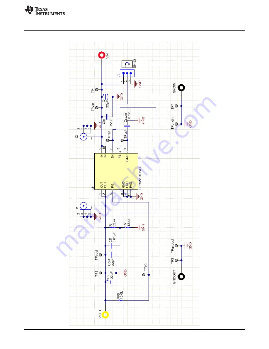
Page 7: ...www ti com LP592201EVM Schematic 7 SNVU532 November 2016 Submit Documentation Feedback Copyright 2016 Texas Instruments Incorporated LP592201EVM User Guide 4 LP592201EVM Schematic ...
Page 8: ...R71A124KA01D 2 GNDIN GNDOUT Standard Banana Jack Insulated Black Keystone 6092 1 VIN Standard Banana Jack Insulated Red Keystone 6091 1 VOUT Standard Banana Jack Insulated Yellow Cinch 108 0907 001 1 J3 Header 3 pin 100 mil spacing 0 100 3 Samtec HTSW 103 07 G S 1 SH J3 Shunt 100 mil Gold plated Black 0 100 2 Samtec SNT 100 BK G 1 R1 Resistor 32 4 kΩ 1 0 125 W 0805 0805 Vishay Dale CRCW080532K4FKE...
Page 9: ... are returned during the warranty period to the address designated by TI and that are determined by TI not to conform to such warranty If TI elects to repair or replace such EVM TI shall have a reasonable time to repair such EVM or provide replacements Repaired EVMs shall be warranted for the remainder of the original warranty period Replaced EVMs shall be warranted for a new full ninety 90 day wa...
Page 10: ... by Industry Canada to operate with the antenna types listed in the user guide with the maximum permissible gain and required antenna impedance for each antenna type indicated Antenna types not included in this list having a gain greater than the maximum gain indicated for that type are strictly prohibited for use with this device Concernant les EVMs avec antennes détachables Conformément à la rég...
Page 11: ...connecting any load to the EVM output If there is uncertainty as to the load specification please contact a TI field representative During normal operation even with the inputs and outputs kept within the specified allowable ranges some circuit components may have elevated case temperatures These components include but are not limited to linear regulators switching transistors pass transistors cur...
Page 12: ...F REMOVAL OR REINSTALLATION ANCILLARY COSTS TO THE PROCUREMENT OF SUBSTITUTE GOODS OR SERVICES RETESTING OUTSIDE COMPUTER TIME LABOR COSTS LOSS OF GOODWILL LOSS OF PROFITS LOSS OF SAVINGS LOSS OF USE LOSS OF DATA OR BUSINESS INTERRUPTION NO CLAIM SUIT OR ACTION SHALL BE BROUGHT AGAINST TI MORE THAN ONE YEAR AFTER THE RELATED CAUSE OF ACTION HAS OCCURRED 8 2 Specific Limitations IN NO EVENT SHALL T...
Page 13: ...esponsible for compliance with all legal regulatory and safety related requirements concerning its products and any use of TI components in its applications notwithstanding any applications related information or support that may be provided by TI Buyer represents and agrees that it has all the necessary expertise to create and implement safeguards which anticipate dangerous consequences of failur...