


A default mode will be restored in the next step, therefore this step is not necessary. It is included, however, to
emphasize the importance of pressing Ctrl+L to load the device at least once after starting TICS Pro, restoring a
mode, or restoring a saved setup using the
File
menu.
See TICS Pro instructions located at
http://www.ti.com/tool/ticspro-sw/
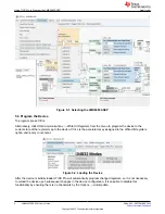
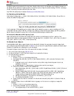
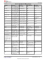
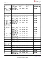
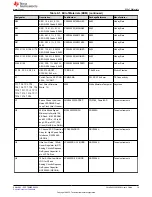
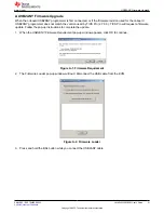
5.4 Restoring a Default Mode
Click
Default configuration → CLKin1 122.88 MHz, OSCin 122.88 MHz, VCO1 2949.12 MHz
. Press
Ctrl+L
to
restore the default configuration.
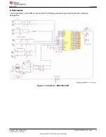
Figure 5-3. Setting the Default Configuration for LMK04832-SEP
For the purpose of this walkthrough, a default mode will be loaded to ensure a common starting point. This
is important because when TICS Pro is closed, the software remembers the last settings used for a particular
device. Again, remember to press
Ctrl+L
as the first step after loading a default mode.
5.5 Visual Confirmation of Frequency Lock
After a default mode is restored and loaded, LED D1 and D2 must illuminate when PLL1 and PLL2 are
locked to the reference clock applied to CLKin1. This assumes PLL1_LD_MUX = PLL1_DLD, PLL2_LD_MUX =
PLL2_DLD, and PLLX_LD_TYPE = Output (Push-Pull).
5.6 Enable Clock Outputs
The LMK04832-SEP offers programmable clock output buffer formats, the evaluation board is shipped with
pre-configured output terminations. Refer to
to see the list of output formats available and what output
formats your hardware is configured for out of the factory.
To measure phase noise at one of the clock outputs (for example, CLKout0):
1. Go to the
Clock Outputs
2. Uncheck
CLKoutX_Y_PD
in the
Clock Output
box to enable the channel.
3. Set the following as needed:
a. For Device Clock:
i.
DCLKX_Y_PD = 0 in Clock Mode Select box
ii. Set Bypass Div (DCLKX_Y_BYP) or Clock Divider (DCLK0_1_DIV) as desired for device clock
frequency:
1. If bypass mode is set, CLKoutX must be set to a CML output format. Bypass mode is not
available on CLKoutY.
2. If Clock Divider = 1, then DCLKX_Y_DCC must be set for clock output.
iii. Phase of the device clock can be adjusted with:
1. Static Digital delay (DCLKX_Y_DDLY) after a SYNC. Digital Delay (DCLKX_Y_DDLY_PD) must
be powered up.
2. Dynamic Digital delay (DDLYdX_EN), then programming DDLYd_STEP_CNT. Digital Delay
(DCLKX_Y_DDLY_PD) must be powered up. Press the
Send
button at top-right of
Clock
Outputs
window to program the DDLYd_STEP_CNT field multiple times.
3. Half Step bit (DCLKX_Y_HS) if DCC & HS (DCLKX_Y_DCC) is set.
4. The Polarity bit (DCLKX_Y_POL)
iv. Select the device clock for CLKoutX or CLKoutY with CLKout#_SRC_MUX = 0 (Device Clock) as
desired.
b. While the phase noise of a SYSREF Clock is typically not of concern, to configure an output for
SYSREF:
i.
SCLKX_Y_PD = 0 in
Clock Mode Select
box
ii. Phase of the SYSREF clock can be adjusted:
1. Local digital delay can be set with SCLKX_Y_DDLY.
Using TICS Pro to Program the LMK04832-SEP
LMK04832SEPEVM User’s Guide
7
Copyright © 2022 Texas Instruments Incorporated


