background image

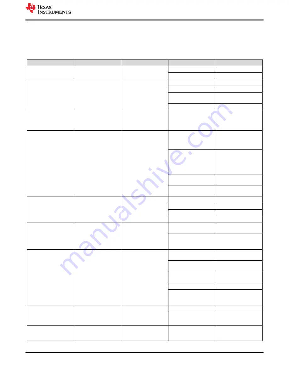
4.4 DRV8329AEVM Configurability Switch Functions

The DRV8329AEVM includes a variety of user-selectable jumpers and unpopulated components on the PCB to 
choose user settings and evaluate the DRV8329A, DRV8329B, DRV8329C, or DRV8329D device. A summary 
of those selectable settings is listed in 

Table 4-2

 (defaults in bold) and can be seen on the board in 

Figure 4-6

.

Table 4-2. User-Selectable Jumpers

Id.

Setting Name

Description

Position

Function

A

nSLEEP switch

Places DRV8329 in sleep 
mode

S2 = Left

Sleep mode

S2 = Right

Operating mode

B

Dead time potentiometer, 
jumper, & resistor

Jumper to enable 
dead time control 
from potentiometer and 
potentiometer used to set 
the resistance for DT pin.

J1 = Populated

DT from pot is enabled

J1 = DNP

DT from pot is disabled

R1 (CW = more DT, CCW 
= less DT)

Sets dead time of gate 
driver outputs

R2

Fixed resistor for DT pin

C

CSA input filter

Input filter to filter 
any Vsense switching 
transients at the current 
sense amplifier inputs.

R45 = R43 = 0 ohm

 C30, 

C31, C32 = DNP

CSA input filtering

D

Power stage MOSFETs 
and passive components

Optional passive 
components for tuning 
power stage, i.e. series 
gate resistors, RC 
snubbers, PVDD-GND 
capacitors, PVDD-LSS 
capacitors

R28, R29, R30, R34, R35, 
R36 = 10 ohm

Series gate resistors 
(GHA, GHB, GHC, GLA, 
GLB, GLC)

R25/C12, R26/C13, R27/
C14, R40/C26, R41/C24, 
R42/C25 = DNP

RC snubbers
(HS FET A, HS FET B, HS 
FET C, LS FET A, LS FET 
B, LS FET C)

C18, C20, C44 = 2.2uF

PVDD-VDRAIN bypass 
capacitor

C21, C22, C23 = 0.01uF

PVDD-LSS bypass 
capacitors

G

CSA gain select

Selects the gain setting of 
the integrated CSA in V/V.

J2 = GND

CSAGAIN = 5 V/V

J2 = 50 k

CSAGAIN = 10 V/V

J2 = 200 k

CSAGAIN = 20 V/V

J2 = DNP

CSAGAIN = 40 V/V

H

HALL_PWR select

Use J6 to supply Hall 
power from AVDD or 
external hall power.

J11 = AVDD

Supplies AVDD to Hall 
power

J11 = EXT

Supply external hall power 
from EXT HALL POWER 
test point.

J

VDSLVL potentiometer, 
select and disable jumpers

Potentiometer to set 
VDSLVL between 0.1 ̶ 2.5 
V, VDSLVL_SEL to select 
voltage source, disable 
jumper to disable VDSLVL

J16 = POT

VDSLVL set from 
potentiometer

J16 = EXT

VDSLVL set from VDS 
EXT test point

J15 = Populated

VDSLVL is disabled (100 
kΩ to GVDD)

J15 = DNP

VDSLVL is enabled

R74 (CCW = higher 
VDSLVL, CW = lower 
VDSLVL)

Sets VDSLVL from 0.1 V ̶ 
2.5 V

K

CSAREF select

Jumper to select CSA 
reference voltage from 
AVDD or an external 
reference source.

J14 = AVDD

CSAREF = AVDD

J14 = EXT

CSAREF = CSAREF EXT 
test point

L

Speed pot

Sets speed of the motor 
when potentiometer is 
enabled in the GUI.

R73 (CW = less speed, 
CCW = more speed)

Sets duty cycle from 0% 
to 100%.

www.ti.com

Hardware and Software Overview

SLVUCF5 – MARCH 2022

Submit Document Feedback

DRV8329AEVM User’s Guide

11

Copyright © 2022 Texas Instruments Incorporated

Summary of Contents for DRV8329AEVM

Page 1: ...8329AEVM GUI 16 6 2 DRV8329x EVM GUI Quick Start Guide 17 6 3 Using the DRV8329AEVM GUI 17 7 Schematics 19 7 1 DRV8329A B 19 7 2 Status LEDs 19 7 3 LaunchPad Connectors and Connections 20 7 4 Power St...

Page 2: ...d Protection schematic 23 List of Tables Table 2 1 DRV8329 device variant names and descriptions default of EVM in bold 4 Table 4 1 Description of DRV8329AEVM LEDs on during power up in bold 10 Table...

Page 3: ...Read the User s Guide before use HOT SURFACE Caution Hot Surface Contact may cause burns Do not touch Please take the proper precautions when operating www ti com Cautions and Warnings SLVUCF5 MARCH...

Page 4: ...vice variant names and descriptions default of EVM in bold Device Name LDO Output DRVOFF pin DT pin and VDSLVL pin PWM_MODE DRV8329A 3 3 V Yes Available 6x DRV8329B 3 3 V Yes Available 3x The DRV8329A...

Page 5: ...Figure 2 1 DRV8329AEVM PCB Layout www ti com Introduction SLVUCF5 MARCH 2022 Submit Document Feedback DRV8329AEVM User s Guide 5 Copyright 2022 Texas Instruments Incorporated...

Page 6: ...applications connect the Hall sensors to the appropriate locations on the 5 pin connector J11 as shown in Figure 4 2 Select AVDD or EXT on jumper J11 to choose the Hall power source voltage 3 Mate the...

Page 7: ...sorless Brushless DC motor A 4 5 V to 60 V power supply or battery is connected to the PVDD and GND terminals The three phases of the BLDC motor connect directly to the OUTA OUTB and OUTC terminals of...

Page 8: ...L F280049C to provide communication between the LaunchPad firmware and GUI as well as the correct installment of the DRV8329AEVM to the J1 J3 and J2 J4 headers of the LaunchPad Hardware and Software O...

Page 9: ...J1 J3 and J2 J4 of LaunchPad Figure 4 4 Micro USB plugged into LaunchPad www ti com Hardware and Software Overview SLVUCF5 MARCH 2022 Submit Document Feedback DRV8329AEVM User s Guide 9 Copyright 202...

Page 10: ...LEDs that are on during power up indicated in bold Figure 4 5 shows the LED locations on the EVM These LEDs all have removable jumpers to reduce power consumed by the EVM Table 4 1 Description of DRV8...

Page 11: ...ors GHA GHB GHC GLA GLB GLC R25 C12 R26 C13 R27 C14 R40 C26 R41 C24 R42 C25 DNP RC snubbers HS FET A HS FET B HS FET C LS FET A LS FET B LS FET C C18 C20 C44 2 2uF PVDD VDRAIN bypass capacitor C21 C22...

Page 12: ...nd replace with the DRV8329B No extra hardware changes are required for 3x PWM operation 4 5 Interfacing DRV8329AEVM and LAUNCHXL F280049C LaunchPad The DRV8329AEVM has 40 pins with different function...

Page 13: ...ot used 20 VDSLVL C_TAP ADCINA1 DACB_OUT VDSLVL from DAC C_TAP for internal use only Table 4 4 Connections for Header J2 on DRV8329AEVM J4 Pin Number DRV8329AEVM Function LAUNCHXL F280049C Function De...

Page 14: ...ensor B from motor 19 nFAULT_49C CSAREF GPIO25 nFAULT signal active low 20 HALLC GPIO59 Hall sensor C from motor Note There are many resistors that are not populated for internal use only Ensure the c...

Page 15: ...three phases from the brushless DC motor to the 3 pin connector J12 on DRV8329AEVM Phases OUTA OUTB and OUTC are labeled in white silkscreen on the PCB top layer If using a sensored algorithm on the L...

Page 16: ...er 1 0 0 DRV8329B https dev ti com gallery view BLDC DRV8329B_EVM_GUI ver 1 0 0 6 1 Connecting to the DRV8329AEVM GUI Follow the instructions in Section 5 and ensure the LAUNCHXL F280049C is connected...

Page 17: ...tch To not use the potentiometer to control the motor speed skip this step 5 Adjust the Duty Cycle slider or enter the duty cycle in the number box to control the speed of the motor from 0 to 100 6 Us...

Page 18: ...RAKING SETTINGS Stop Motor Stops the motor when toggled according to the braking method in the drop down menu The two methods are brake turn on all low side MOSFETs and coast float all MOSFETs CSA SET...

Page 19: ...A B Figure 7 1 DRV8329A B schematic 7 2 Status LEDs Figure 7 2 Status LEDs schematic www ti com Schematics SLVUCF5 MARCH 2022 Submit Document Feedback DRV8329AEVM User s Guide 19 Copyright 2022 Texas...

Page 20: ...ors schematic Figure 7 4 LaunchPad connections schematic 7 4 Power Stage and MOSFETs Figure 7 5 Powerstage and MOSFETs schematic Schematics www ti com 20 DRV8329AEVM User s Guide SLVUCF5 MARCH 2022 Su...

Page 21: ...schematic 7 6 Hall Sensor and Hall Power selection Figure 7 7 Hall Sensor and Hall Power selection schematic www ti com Schematics SLVUCF5 MARCH 2022 Submit Document Feedback DRV8329AEVM User s Guide...

Page 22: ...lectors and Analog Control Interface schematic 7 8 Dead Time and CSA Gain Selection Figure 7 9 Dead time and CSA gain selection schematic Schematics www ti com 22 DRV8329AEVM User s Guide SLVUCF5 MARC...

Page 23: ...Sense and Protection Figure 7 10 Voltage Sense and Protection schematic www ti com Schematics SLVUCF5 MARCH 2022 Submit Document Feedback DRV8329AEVM User s Guide 23 Copyright 2022 Texas Instruments I...

Page 24: ...change without notice TI grants you permission to use these resources only for development of an application that uses the TI products described in the resource Other reproduction and display of thes...

Reviews: