


EVM Operation
www.ti.com
3.3
Digital Control Interface
The DAC8881 supports the standard high-speed SPI™ serial interface to communicate with
microprocessors or DSP devices. The EVM incorporates pass-through connectors to accommodate the
digital control interface to the DAC8881 device via the J2 (top side) and P2 (bottom side) header/socket
connectors. The signals of these pass-through connectors are listed in
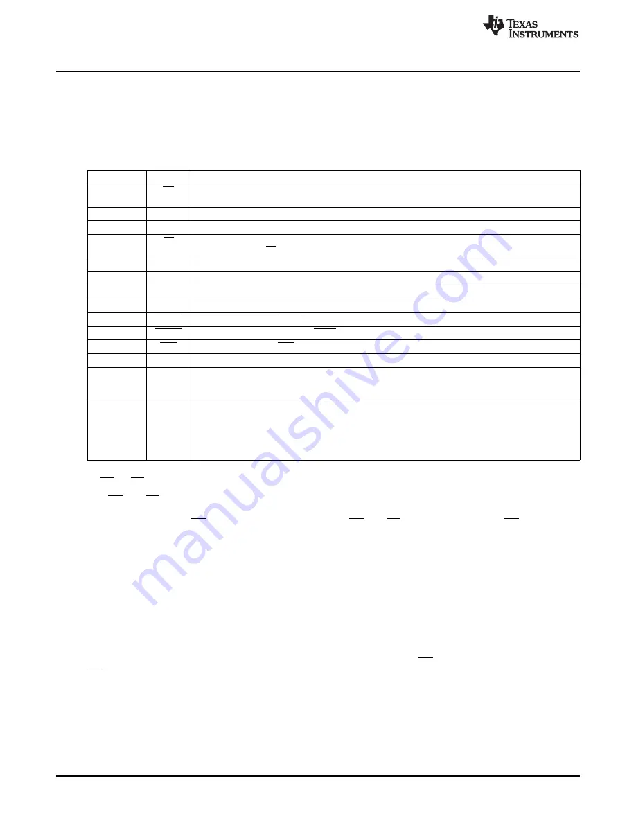
Table 3. Digital Control Interface Signal Mapping for J2/P2 Header/Socket Connectors
Pin Number
Signal
Function
J2.1/P2.1
CS
Primary synchronization and device enable input for the DAC8881. Host microcontroller STE signal for
SPI interface.
J2.3/P2.3
SCLK
Serial interface clock.
J2.5/P2.5
CLKR
Unused.
J2.7/P2.7
FS
Secondary synchronization and device enable input for the DAC8881. Host microcontroller STE signal
for SPI interface or FS signal from DSP host system.
J2.9/P2.9
FSR
Unused.
J2.11
SDO
Serial data output.
P2.11
SDI
Serial data input.
J2.13/P2.13
DR
Unused.
J2.15/P2.15
LDAC1
GPIO signal to control LDAC for DAC output latch update.
J2.17/P2.17
LDAC2
Alternate GPIO signal to control LDAC for DAC output latch update.
J2.19/P2.19
RST
GPIO signal to control RST for DAC reset function.
J2.2/P2.2
PDN
GPIO signal to control PDN for hardware powerdown.
J2.4/P2.4
GND
Signal ground.
J2.10/P2.10
J2.18/P2.18
J2.6/P2.6
GPIOs
Unused.
J2.8/P2.8
J2.12/P2.12
J2.14/P2.14
J2.16/P2.16
J2.20/P2.20
3.3.1
CS or FS Signal
The CS and FS signals of the EVM are interchangeable and the signal used depends on the host
controller that is selected to communicate with the DAC8881EVM. Either signal can be chosen to drive the
DAC8881 chip select (CS) pin. The basic function of the CS and FS signals is to drive the CS pin of the
DAC8881 to enable the device communication port and to synchronize the data input into the device
immediately following its high-to-low transition. This signal must be held low while the host processor is
accessing the DAC. The low-to-high transition of this signal transfers the contents of the serial shift
register to the DAC input register.
3.3.2
SCLK Signal
The SCLK signal is the clock necessary to load the serial data input into the DAC serial shift register. The
serial clock rate can operate at speeds up to 50MHz. The 16-bit data is shifted out of the bus master
synchronously on the falling edge of SCLK and latched on the rising edge of SCLK into the DAC serial
shift register. The most significant bit (MSB) is the first bit that is output to the DAC. After 16-bits are
transferred or 16 SCLK cycles are generated, the bus master takes the CS signal high immediately. If the
CS signal is held low and more than 16 SCLK cycles are applied, the last SCLK cycle is considered the
location of the least significant bit (LSB) of the 16-bit word that is loaded into the DAC serial shift register.
Hence, the user must know the data word alignment with respect to SCLK or else the data input can
become corrupted. If this happens, simply reload the DAC latch with the new 16-bit word.
12
DAC8881 Evaluation Module
SLAU257A – September 2008 – Revised November 2009
Copyright © 2008–2009, Texas Instruments Incorporated