www.ti.com
Layout
25
SNAU244 – July 2019
Submit Documentation Feedback
Copyright © 2019, Texas Instruments Incorporated
Schematic and Layout
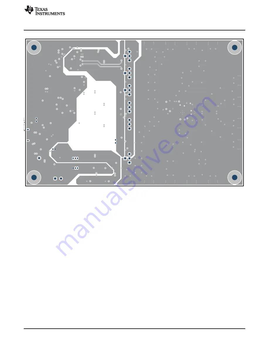
Figure 4-11. PCB Layer 3: Middle Layer
Page 1: ...CDCE6214 Q1EVM User s Guide Literature Number SNAU244 July 2019...
Page 2: ...tions 9 2 1 Input Configuration 9 2 1 1 Input Selection 9 2 1 2 Crystal Input 10 2 2 PLL Configuration 10 2 3 SSC DCO and ZDM Modes 10 2 4 Output Configuration 10 2 5 1 8 V and 3 3 V Power Supply 11 3...
Page 3: ...V to 3 3 V Four differential outputs with multi mode output buffers One LVCMOS bypass output Crystal oscillator with integrated load capacitance and configurable gain LVCMOS or AC coupled differential...
Page 4: ...llow the instructions and install the TICS Pro software on PC in a default directory To launch TICS Pro go to Select Device in the toolbar and select Clock Generator Jitter Cleaner Single Loop CDCE621...
Page 5: ...1 of J9 Short pin 2 of J10 and pin 1 of J13 The purpose of this step is to connect SCL and SDA pins of DUT to the on board microcontroller in order to enable I2C programming 4 Short pin 1 and 2 of J12...
Page 6: ...Documentation Feedback Copyright 2019 Texas Instruments Incorporated Quick Start 1 4 Scan I2C Bus Click the Scan I2C Bus in the small toolbar Look for the Device found at 0x68 Address will be updated...
Page 7: ...lt and Check Lock Status NOTE Hover over a register to read the register description in the bottom left pane of the TICS Pro window In the toolbar go to Default configurations Default Startup From the...
Page 8: ...e format of output 1 to CMOSPN to select the CMOS format output for both OUT1_P and OUT1_N then connect the SMA_OUT1P J15 or SMA_OUT1N J17 to an oscilloscope With 50 DC termination see the 100 MHz and...
Page 9: ...nd pin 4 REFSEL Register R2 1 0 overrides pin 4 To enable pin control for input selection go to TICS Pro Input page and set register REF_SEL to Pin Pull pin REFSEL low SECREF or high PRIREF using jump...
Page 10: ...citance selected is 9 8 pF the capacitance is 9 8 pF at both the source and drain Crystal vendors typically refer to load capacitance as effective series capacitance seen by the crystal So when 9 8 pF...
Page 11: ...e the 1 8 V LDOs short pin 2 and 3 of J26 To disable the 1 8 V LDOs remove the jumper for J26 To use 3 3 V LDO the designer must first populate the four 0 resistors R64 R66 R68 and R70 After the resis...
Page 12: ...p Figure 3 1 USB2ANY Connection 3 1 2 Upgrade USB2ANY Firmware If you are having issues with the USB2ANY you can reload the firmware using the USB2ANY firmware loader application You can download it a...
Page 13: ...rk the board to enable 3 3 V LDOs Follow these steps and refer to Figure 3 2 to configure the jumpers Short J23 Short pins 2 and 3 of J25 and remove jumper for J26 to enable 3 3 V LDOs and disable 1 8...
Page 14: ...Texas Instruments Incorporated Frequently Asked Questions FAQ 3 2 2 Connect SDA SCL and GND to USB2ANY Refer to Figure 3 3 and connect the SDA SCL and GND to pin 1 pin 2 and pin 5 of USB2ANY J4 in Fi...
Page 15: ...July 2019 Submit Documentation Feedback Copyright 2019 Texas Instruments Incorporated Schematic and Layout Chapter 4 SNAU244 July 2019 Schematic and Layout 4 1 Schematic Figure 4 1 Schematic Page 1 C...
Page 16: ...Schematic www ti com 16 SNAU244 July 2019 Submit Documentation Feedback Copyright 2019 Texas Instruments Incorporated Schematic and Layout Figure 4 2 Schematic Page 2 USB...
Page 17: ...www ti com Schematic 17 SNAU244 July 2019 Submit Documentation Feedback Copyright 2019 Texas Instruments Incorporated Schematic and Layout Figure 4 3 Schematic Page 3 Power...
Page 18: ...Schematic www ti com 18 SNAU244 July 2019 Submit Documentation Feedback Copyright 2019 Texas Instruments Incorporated Schematic and Layout Figure 4 4 Schematic Page 4 Power Filter Distribution...
Page 19: ...www ti com Schematic 19 SNAU244 July 2019 Submit Documentation Feedback Copyright 2019 Texas Instruments Incorporated Schematic and Layout Figure 4 5 Schematic Page 5 Level Shifter...
Page 20: ...Schematic www ti com 20 SNAU244 July 2019 Submit Documentation Feedback Copyright 2019 Texas Instruments Incorporated Schematic and Layout Figure 4 6 Schematic Page 6 Input and Clock Generator...
Page 21: ...www ti com Schematic 21 SNAU244 July 2019 Submit Documentation Feedback Copyright 2019 Texas Instruments Incorporated Schematic and Layout Figure 4 7 Schematic Page 7 Outputs...
Page 22: ...Schematic www ti com 22 SNAU244 July 2019 Submit Documentation Feedback Copyright 2019 Texas Instruments Incorporated Schematic and Layout Figure 4 8 Schematic Page 8 EVM Hardware...
Page 23: ...www ti com Layout 23 SNAU244 July 2019 Submit Documentation Feedback Copyright 2019 Texas Instruments Incorporated Schematic and Layout 4 2 Layout Figure 4 9 PCB Layer 1 Top Layer Composite...
Page 24: ...Layout www ti com 24 SNAU244 July 2019 Submit Documentation Feedback Copyright 2019 Texas Instruments Incorporated Schematic and Layout Figure 4 10 PCB Layer 2 Middle Layer...
Page 25: ...www ti com Layout 25 SNAU244 July 2019 Submit Documentation Feedback Copyright 2019 Texas Instruments Incorporated Schematic and Layout Figure 4 11 PCB Layer 3 Middle Layer...
Page 26: ...Layout www ti com 26 SNAU244 July 2019 Submit Documentation Feedback Copyright 2019 Texas Instruments Incorporated Schematic and Layout Figure 4 12 PCB Layer 4 Bottom Layer Composite...
Page 27: ...e resources are subject to change without notice TI grants you permission to use these resources only for development of an application that uses the TI products described in the resource Other reprod...