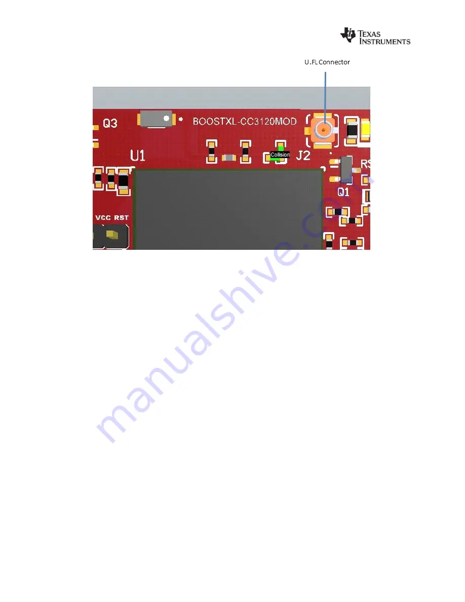
background image


Figure


7

5:


U.FL


Connector


7.5


Connecting


to


PC


Using


the


CC31XXEMUBOOST


7.5.1


CC31XXEMUBOOST


7.5.1.1


Overview


The


CC31XXEMUBOOST


is


designed


to


connect


the


BoosterPack


module


to


a


PC


using


a


USB


connection.


This


updates


the


firmware


patches,


which


are


stored


in


the


serial


flash,


on


the


BoosterPack;


and


in


software


development


using


SimpleLink


Studio.


The


board


is


also


used


for


measuring


the


RF


performance


using


a


software


tool


named


RadioTool.


7.5.1.2


Hardware


details


Figure


7

6


shows


the


CC31XXEMUBOOST


board.


Summary of Contents for CC3120MODRNMMOB

Page 1: ...o incorporate the CC3120MOD module into their final product It also provided information how to run the BOOSTXL CC3120MOD SimpleLink BoosterPack to evaluate the CC3120MOD module Contents 1 Overview 3 1 1 General Features 7 1 2 Key Benefits 8 1 3 Key Benefits 10 2 Connectors and Jumpers 10 2 1 Connectors and Jumpers 11 2 2 Jumper Settings 12 2 3 2x20 Pin connector assignment 12 3 Electrical Charact...

Page 2: ...cation and Statement 31 2 1 FCC 32 2 2 CAN ICES 3 A NMB 3 A Certification and Statement 32 2 3 End Product Labeling 33 2 4 Device Classifications 34 2 5 FCC Definitions 34 2 6 Simultaneous Transmission Evaluation 35 3 EU Certification and Statement 35 3 1 RF Exposure Information MPE 35 3 2 Simplified DoC statement 35 3 3 Waste Electrical and Electronic Equipment WEEE 36 3 4 OEM Host manufacturer r...

Page 3: ...the CC3120MOD module PM MAC PHY SPI WRF BGN HIB VBAT F RF_ANT1 2 3 3 6V CC3X20 UART nReset 32Mbit SFlash 32 768 kHz 40Mhz Figure 1 1 CC3120MOD Functional Block Diagram Figure 1 2 shows a functional block diagram of the BOOSTXL CC3120MOD SimpleLink BoosterPack ...

Page 4: ...Figure 1 2 Functional block diagram of the BOOSTXL CC3120MOD Figure 1 3 shows the hardware implementation of the BOOSTXL CC3120MOD CC3120MODRNMMOB ...

Page 5: ...Figure 1 3 Hardware implementation of the BOOSTXL CC3120MOD Figure 1 4 shows the Top Overlay of the BOOSTXL CC3210MOD SimpleLink BoosterPack ...

Page 6: ...Figure 1 4 BOOSTXL CC3120MOD Top Overlay Figure 1 5 shows the Top Solder of the BOOSTXL CC3210MOD SimpleLink BoosterPack ...

Page 7: ...leLink Launchpad and BoosterPack architecture Built in chip antenna Optional U FL connector for external antennas or conducted based testing Power from an onboard LDO by using the USB or 3 3 Vconnector form the LaunchPad MCU Three push buttons Two LEDs Jumper for current measurements with provisions to mount a 0 1 ohm resistor for measurement with a voltmeter 32 Mbit serial Flash Two layer PCB ...

Page 8: ...ing up to Four Stations o Wi Fi Direct Client Group Owner o WPA2 Personal and Enterprise Security WEP WPA WPA2 PSK WPA2 Enterprise 802 1x IPv4 and IPv6 TCP IP Stack o Industry Standard BSD Socket Application Programming Interfaces APIs 16 Simultaneous TCP or UDP Sockets 6 Simultaneous TLS and SSL Sockets IP Addressing Static IP LLA DHCPv4 and DHCPv6 With Duplicate Address Detection DAD SimpleLink ...

Page 9: ...ted DC DC Converters Support a Wide Range of Supply Voltage VBAT Wide Voltage Mode 2 3 V to 3 6 V o Advanced Low Power Modes Shutdown 1 μA Hibernate 6 μA Low Power Deep Sleep LPDS 115 μA RX Traffic 59 mA at 54 OFDM TX Traffic 229 mA at 54 OFDM Maximum Power Idle Connected MCU in LPDS 690 μA at DTIM 1 Additional Integrated Components on Module o 40 0 MHz Crystal With Internal Oscillator o 32 768 kH...

Page 10: ...ances Access Control Security Systems Smart Energy Industrial Control Smart Plug and Metering Wireless Audio IP Network Sensor Nodes Asset Tracking Medical Devices 2 Connectors and Jumpers Figure 2 1 shows the top view of the BOOSTXL CC3120MOD SimpleLink BoosterPack Figure 2 1 BOOSTXL CC3120MOD Top View Figure 2 2 shows the bottom view of the BOOSTXL CC3120MOD SimpleLink BoosterPack ...

Page 11: ...g the firmware over a universal asynchronous receiver transmitter UART Table 2 1 BOOSTXL CC3120MOD push buttons Table 2 2 lists the LEDs on the BOOSTXL CC3120MOD Reference Colour Usage Comments D5 RED PWR indication ON when the 3 3 V power is provided to the board D1 Yellow nRESET This LED indicates the state of the nRESET pin If this LED is glowing the device is f ti l D6 Green nHIB This LED indi...

Page 12: ...eset Pullup For keeping the reset up J2 RF Test U FL connector for conducted testing in the lab Using this requires an ECO to be made to the board by swapping two resistors Table 2 3 BOOSTXL CC3120MOD jumper settings 2 3 2x20 Pin connector assignment Table 2 4 lists the outer row connectors of the two 20 pin headers Note All signals are 3 3V CMOS logic levels and are referred with respect to the C...

Page 13: ... row pin connectors 3 Electrical Characteristics For electrical characteristics see the CC3120MOD SimpleLink Wi Fi CERTIFIED Network Processor Internet of Things Module Solution for MCU Applications Datasheet 4 Antenna Characteristics The BOOSTXL CC3120MOD contains an on chip antenna For information on the antenna VSWR efficiency and electrical characteristics please see http ds yuden co jp TYCOMP...

Page 14: ... schematic 5 2 Bill of Materials BOM The CC3120MOD main engine area reference BOM is show in Table 5 1 below The full BOOSTXL CC3120MOD reference BOM can be found at http www ti com lit zip swrc339 Table 5 1 CC3120MOD Engine area reference BOM ...

Page 15: ...sk with regulatory certifications for FCC IC CE MIC and SRRC Moreover TI recommends customers follow the guidelines described in this section to achieve similar performance 6 1 Board Layout The reference layout consists of a 2 layer design Figure 6 1 shows BOOSTXL CC3120MOD Top layer Figure 6 1 BOOTXL CC3120MOD Top Layer Figure 6 2 shows the BOOSTXL CC3120MOD Bottom layer ...

Page 16: ...ere the module is mounted RF traces must have 50 Ω impedance RF trace bends must be made with gradual curves and 90 degree bends must be avoided RF traces must not have sharp corners There must be no traces or ground under the antenna section RF traces must have via stitching on the ground plane beside the RF trace on both sides RF traces must be as short as possible The antenna RF traces and the ...

Page 17: ...ance from the device A poor layout can cause low output power EVM degradation sensitivity degradation and mask violations Figure 6 3 shows the RF placement and routing of the CC3120MOD module Figure 6 3 RF Section Layout For optimal RF performance ensure the copper cut out on the top layer under the RF BG pin pin 31 is as shown in Figure 6 4 below Figure 6 4 Top layer copper pull back on RF pads ...

Page 18: ...tuning the antenna because this can impact the impedance 5 Ensure that the antenna impedance is 50 Ω because the device is rated to work only with a 50 Ω system 6 In case of printed antenna ensure that the simulation is performed with the solder mask in consideration 7 Ensure that the antenna has a near omni directional pattern 8 The feed point of the antenna is required to be grounded This is onl...

Page 19: ...3 and 4 layer boards in Table 6 4 Table 6 3 Recommended PCB Values for 2 Layer Board L1 to L2 42 1 mils Table 6 4 Recommended PCB Values for 4 layer Board L1 to L2 16 mils 7 BOOSTXL CC3120MOD Operational Setup and Testing The SimpleLink Wi Fi CC3120MOD wireless network processor provides the flexibility to add Wi Fi to any microcontroller MCU This user guide explains the various configurations of ...

Page 20: ...20MOD BoosterPack o MSP EXP432P401R LaunchPad BOOSTXL CC3120MOD CC31XXEMUBOOST which contains the following o SimpleLink Wi Fi CC3120 BoosterPack o Advanced Emulation BoosterPack 7 1 Power The board is designed to accept power from a connected LaunchPad kit or through the CC31XXEMUBOOST board Some of the LaunchPad kits are not capable of sourcing the peak current requirements of Wi Fi which may be...

Page 21: ...d kit with only 20 pins the USB connector on the BOOSTXL CC3120MOD should be used to provide the LDO input as shown in Figure 7 1 Figure 7 1 3 3 V Power from MCU LaunchPad Kit Figure 7 2 USB Location on BoosterPack Module ...

Page 22: ...er Figure 7 3 3 3 V Power From LDO 7 2 Measuring the CC3120MOD Current Draw 7 2 1 Low Current Measurements Hibernate and LPDS To measure the current draw of the CC3120RM and the serial flash a jumper is provided on the board labeled J6 By removing this jumper one can place an ammeter into this path and the current can be observed This method is recommended for measuring LPDS and hibernate currents...

Page 23: ...surements To measure active current in a profile form it is recommended to use a 0 1 Ω 1 resistor on the board and measure the differential voltage across it see Figure 7 4 This can be done using a voltmeter or an oscilloscope for measuring the current profile ...

Page 24: ...4 Performing Conducted Tests The BoosterPack board by default ships with the RF signal connected to the onboard chip antenna Figure 7 5 shows that there is a U FL connector on the board that can be used for conducting testing or to connect an external antenna This requires a board modification mounting C4 and depopulating C5 as shown in Figure 7 5 ...

Page 25: ...he BoosterPack module to a PC using a USB connection This updates the firmware patches which are stored in the serial flash on the BoosterPack and in software development using SimpleLink Studio The board is also used for measuring the RF performance using a software tool named RadioTool 7 5 1 2 Hardware details Figure 7 6 shows the CC31XXEMUBOOST board ...

Page 26: ... Type Usage Comments 1 D2XX SPI port for SL Studio 2 D2XX GPIO for SL Studio Control the nRESET nHIB IRQ 3 VCP COM port for Flash programming 4 VCP NWP Network processor logger output Used with specific tools to analyze the network processor logs For TI use only Table 7 1 COM and D2XX Ports The third COM port in the list see Figure 7 7 is used for the Flash programming ...

Page 27: ...is package is available as part of the SDK release and is located at Install Path CC3120 sdk tools cc31xx_board_drivers The install path is usually C ti CC3120SDK 7 5 2 Connecting to Board Figure 7 8 shows the connection of the CC3120 BoosterPack module to the EMUBOOST board The connectors should be aligned carefully as it does not have polarity protection and the Flash can be erased as a result T...

Page 28: ...eader pins are bent before connecting the boards 7 5 3 BOOSTXL CC3120MOD Jumper Settings Table 7 3 specifies the jumpers to be installed on the BOOSTXL CC3120RM before pairing with the EMUBOOST board No Jumper Settings Notes 1 J8 1 2 Power the BoosterPack from the EMU BOOST The jumper shall be placed so that it is nearer to the edge of the PCB 3 J6 short No current measurement Table 7 3 BOOSTXL CC...

Page 29: ...ing the standard 2x20 pin connectors The jumper settings needed for this connection are the same as those needed for the EMUBOOST board as described in section 7 5 4 Ensure that the Pin1 of the 2x20 pins are aligned correctly before pairing Figure 7 9 illustrates the connected setup Note that the USB cable is directly connected to the BoosterPack Module to power it only For debugging the USB cable...

Page 30: ...e configured as shown in Figure 7 9 when the power is supplied from the on board USB connector Figure 7 9 Jumper Configuration when working with Launchpad kit NOTE Since there are two power sources in this setup it is important to follow the power up sequence Always power the BoosterPack module before powering the LaunchPad kit Connect USB ...

Page 31: ...he end user is unable to change the region of operation at any time NOTE The maximum RF power transmitted in each WLAN 2 4GHz band is 18 dBm 2 FCC IC Certification and Statement This device is intended for OEM integrators under the following conditions The antenna must be installed such that 20 cm is maintained between the antenna and users The transmitter module may not be co located with any oth...

Page 32: ...requency energy and if not installed and used in accordance with the instructions may cause harmful interference to radio communications However there is no guarantee that interference will not occur in a particular installation If this equipment does cause harmful interference to radio or television reception which can be determined by turning the equipment off and on the user is encouraged to tr...

Page 33: ...blies pour un environnement non contrôlé Cet équipement doit être installé et utilisé avec un minimum de 20 cm de distance entre la source de rayonnement et votre corps This radio transmitter 451I CC3120MOD has been approved by Industry Canada to operate with the antenna types listed in Section 3 5 of this document with the maximum permissible gain indicated Antenna types not included in this list...

Page 34: ...ll be able to assist in determining the appropriate device category for your host product and if a KDB or PBA must be submitted to the FCC Note the module you are using has been granted modular approval for mobile applications Portable applications may require further RF exposure SAR evaluations It is also likely that the host module combination will need to undergo testing for FCC Part 15 regardl...

Page 35: ...mitting antennas is 20 cm Or Antenna separation distance and MPE compliance requirements for ALL simultaneous transmitting antennas have been specified in the application filing of at least one of the certified transmitters within the host device In addition when transmitters certified for portable use are incorporated in a mobile host device the antenna s must be 5 cm from all other simultaneous ...

Page 36: ...all the essential requirements of the RED before it can be placed on the EU market This includes reassessing the transmitter module for compliance with the Radio and EMF essential requirements of the RED This module must not be incorporated into any other device or system without retesting for compliance as multi radio and combined equipment 3 5 Antenna specifications In all cases assessment of th...

Page 37: ...other simultaneous transmission radio is installed in the host platform together with this module or above restrictions cannot be kept a separate RF exposure assessment and CE equipment certification is required ...

Reviews: