background image

BUF18830EVM Software

www.ti.com

20

SBOU103A – April 2011 – Revised May 2016

Submit Documentation Feedback

Copyright © 2011–2016, Texas Instruments Incorporated

BUF18830EVM User Guide and Software Tutorial

2.3.6

Save to File Button

The register configurations of the BUF18830 DACs are displayed in both analog voltage and in
hexadecimal (see

Figure 14

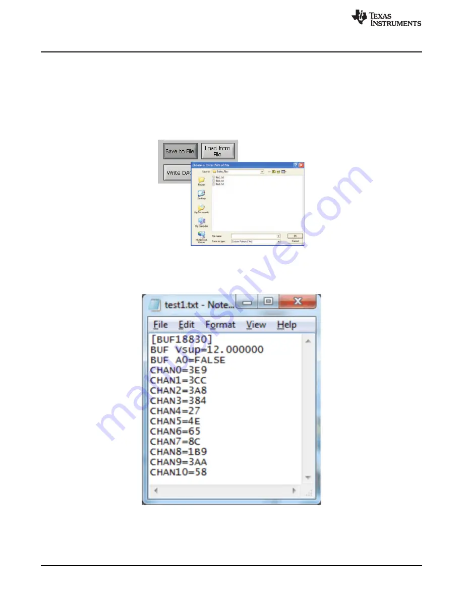
). The DAC codes (that is, gamma voltages) can be saved into a text file by

using the

Save to File

button.

Pressing the

Save to File

button opens a file-save dialog box similar to that shown in

Figure 20

Pressing

the folder icon creates a new folder on your PC. It is a good idea to create a directory exclusively for
BUF18830 DAC code (that is, gamma voltage) files. Enter a unique file name in the

File name

field to

store your BUF18830 register information. Press the

OK

button to save the file.

Figure 20. Save to File Dialog Box Button and Window

Saved BUF18830 DAC codes (gamma voltages) exist in a text file that can be opened in a text editor, as

Figure 21

illustrates.

Figure 21. File Format of Saved Data

Summary of Contents for BUF18830EVM

Page 1: ...ard PCB layout drawings and a parts list for the EVM Contents 1 Overview 2 2 BUF18830EVM Software 14 3 BUF18830EVM Documentation 24 List of Figures 1 Hardware Included with BUF18830EVM Kit 3 2 BUF18830EVM Hardware Setup 4 3 BUF18830EVM Board Block Diagram 5 4 USB_DIG_Platform Block Diagram 7 5 Typical Hardware Connections for BUF18830EVM 8 6 Connecting External Power to the EVM 9 7 Connecting the ...

Page 2: ...Functions 12 5 Bill of Materials 26 1 Overview The BUF18830 is a programmable gamma voltage generator and VCOM calibrator This device offers 18 programmable gamma channels and two programmable VCOM channels making it ideal for 10 bit source TFT LCD reference drivers The BUF18830EVM is a platform for evaluating the performance of the BUF18830 under various signal reference and supply conditions Thi...

Page 3: ...ncluded hardware Contact the Texas Instruments Product Information Center nearest you if any component is missing It is highly recommended that you also check the BUF18830 product folder on the TI web site at www ti com to verify that you have the latest versions of the related software Table 1 BUF18830EVM USB Kit Contents Item Quantity BUF18830 PCB Test Board 1 USB_DIG_Platform PCB 1 USB Cable 1 ...

Page 4: ...s current at the time of the writing of this document Newer revisions may be available from the TI web site or call the Texas Instruments Literature Response Center at 800 477 8924 or the Product Information Center at 972 644 5580 When ordering identify the document by both title and literature number Related Documentation Document Literature Number BUF18830 Product Data Sheet SBOS524 USB_DIG_Plat...

Page 5: ...Instruments Incorporated BUF18830EVM User Guide and Software Tutorial Theory of Operation for BUF18830 Hardware A block diagram of the BUF18830 test board hardware setup is shown in Figure 3 The functionality of the PCB is such that it provides connections to the I2 C interface and general purpose inputs outputs GPIOs on the USB_DIG_Platform board It also provides connection points for external co...

Page 6: ...onnection 5 N C No connection 6 N C No connection 7 N C No connection 8 N C No connection 9 I2C_SCK No connection 10 I2C_SDA2 No connection 11 N C No connection 12 I2C_SCK_ISO I2 C clock signal SCL channel 1 can be disconnected using a switch 13 I2C_SDA_ISO I2 C data signal SDA channel 1 can be disconnected using a switch 14 N C No connection 15 N C No connection 16 N C No connection 17 VDUT Switc...

Page 7: ... details of its operation are included in a separate document SBOU058 available for download at www ti com The block diagram shown in Figure 4 gives a brief overview of the platform The primary control device on the USB_DIG_Platform is the TUSB3210 The barrel connector cable assembly included in the EVM kit can be used to connect an external power supply to the USB DIG through J5 Figure 4 USB_DIG_...

Page 8: ... Connections To set up the BUF18830EVM hardware connect the two PCBs of the EVM together that is the BUF18830 Test Board and USB_DIG_Platform board via a 25 pin DSUB connector and apply a power source The external connections may be the real world system that the BUF18830 will be incorporated into Figure 5 illustrates the typical hardware connections Figure 5 Typical Hardware Connections for BUF18...

Page 9: ...nections may cause intermittent operation Connecting Power After the two parts of the BUF18830EVM are conjoined connect a 6V wall supply to the USB_DIG_Platform board as Figure 6 shows Always connect power before connecting the USB cable If you connect the USB cable before connecting the power the computer will attempt to communicate with an unpowered device that will not be able to respond In add...

Page 10: ...und New Hardware USB Device pop up dialog The pop up window typically changes to Found New Hardware USB Human Interface Device This pop up indicates that the device is ready to be used The USB_DIG_Platform uses the human interface device drivers that are part of the Microsoft Windows operating system Figure 7 Connecting the USB Cable to the USB_DIG_Platform In some cases the Windows Add Hardware W...

Page 11: ...orial BUF18830EVM Default Jumper Settings Figure 9 shows the default jumper configuration for the BUF18830EVM In general the jumper settings of the USB_DIG_Platform will not need to be changed You may want to change some of the jumpers on the BUF18830EVM board to match your specific configuration For example you may wish to set a specific I2 C address Figure 9 BUF18830EVM Default Jumper Settings ...

Page 12: ...e USB_DIG_Platform 1 CAUTION Adjusting outside of this range will damage the EVM Table 4 USB_DIG_Platform Jumper Functions Jumper Default Purpose JUMP1 EXT This jumper selects external power or bus power External power is applied on J5 or T3 9V dc Bus power is 5V from the USB bus External power is typically used because the USB Bus power is noisy JUMP2 EXT Same as JUMP1 JUMP3 EE ON This jumper det...

Page 13: ...s turned on or off When JMP3 is set in the EXT position an external supply connected to terminal T1 can be used to provide the digital supply voltage for the BUF18830 BUF18830 Device Placement The BUF18830EVM allows the user two separate locations on the board where the BUF18830 test device can be installed The U1 location on the BUF18830 test board is a 38 pin QFN test socket that allows the user...

Page 14: ...an also generate an active feedback signal that is forwarded to Vcom FB2 through resistor R3 Resistors R2 and R3 are used together to adjust the gain of the feedback where the gain is equal to the value of R2 R3 Higher gain results in faster Vcom2 voltage regulation but produces additional noise and power dissipation the gain should be adjusted accordingly to your circuit needs 2 BUF18830EVM Softw...

Page 15: ...he Texas Instruments and National Instruments license agreements the progress bar opens and shows the installation of the software as Figure 12 illustrates Once the installation process is completed click Finish Figure 11 BUF18830EVM License Agreements Figure 12 BUF18830EVM Software Installation Progress 2 3 Software Description and Set Up The BUF18830EVM software allows the user to read and write...

Page 16: ...e should appear if the BUF18830EVM is functioning properly Figure 14 BUF18830EVM Software Interface Figure 15 shows an error that pops up if the computer cannot communicate with the EVM If you receive this error first check to see that the USB cable is properly connected on both ends This error can also occur if you connect the USB cable before the USB_DIG_Platform power source Another possible so...

Page 17: ... see Section 1 8 jumper JMP2 is used to set the I2 C address pin of the BUF18830 Figure 16 shows how the hardware and software must both be set to allow for communication between the BUF18830EVM and the software Without jumper JMP2 and the software address button configured correctly the software will not be able to communicate with the BUF18830 device Figure 16 JMP2 Setting For Logic 1 When JMP2 ...

Page 18: ...own in Figure 18 Figure 18 Measuring and Entering Power Supply Voltage The voltage out of each DAC is calculated according to the VS value entered The calculation is performed according to Equation 1 1 For example changing the value in the channel 6 cell immediately changes the output of channel 6 to 0 996V Example Channel 6 Code 44 hexadecimal 68 decimal 2 3 3 Read DAC Button By pressing the Read...

Page 19: ...nd then press the Write DAC button to change all of the output voltage of all of the channels at one time When the Auto Write feature is enabled no change occurs to the output voltages when the Write DAC button is pressed No change occurs because after the text box for a given channel has been updated as soon as another item in the software is clicked the Auto Write feature automatically performs ...

Page 20: ... the Save to File button Pressing the Save to File button opens a file save dialog box similar to that shown in Figure 20 Pressing the folder icon creates a new folder on your PC It is a good idea to create a directory exclusively for BUF18830 DAC code that is gamma voltage files Enter a unique file name in the File name field to store your BUF18830 register information Press the OK button to save...

Page 21: ...ell to be edited Click a second time and the cell turns from blue to black and allows the user to type the updated voltage in the cell The hexadecimal DAC codes can be entered in the Code column in the same manner Another method of changing the voltage of a DAC or VCOM channel is through the use of the slider on the main software window There is only a single slider that is used for all channels I...

Page 22: ...settings to determine what the optimal settings must be for a given application When the Run Batch button is pressed a new dialog box displays as Figure 23 shows The delay time is the amount of time allowed between loading new configurations into the BUF18830 DUT Use the Single Step Up and Single Step Down buttons to step through the selected files manually The currently selected file name is disp...

Page 23: ...p a display panel that allows you to adjust each channel using a set of graphical sliders as shown in Figure 24 Simply drag the slider to adjust the desired channel output The DAC code and corresponding output value of each channel change automatically This function is similar to the slider present on the primary BUF18830EVM software window that changes based on the channel that highlighted as dis...

Page 24: ...tware Tutorial 3 BUF18830EVM Documentation This section contains the complete bill of materials and schematic diagram for the BUF18830EVM Documentation information for the USB_DIG_Platform can be found in the USB_DIG_Platform User s Guide SBOU058 available at the TI web site at http www ti com 3 1 Schematic Figure 25 shows the schematic for the BUF18830EVM Figure 25 BUF18830EVM Schematic ...

Page 25: ...ed May 2016 Submit Documentation Feedback Copyright 2011 2016 Texas Instruments Incorporated BUF18830EVM User Guide and Software Tutorial 3 2 PCB Layouts Figure 26 shows the PCB component layout of the BUF18830EVM test board Figure 26 BUF18830EVM PCB Component Layout ...

Page 26: ... Position 30GOLD with threaded inserts and board locks AMP Tyco Electronics 5747842 4 10 3 T1 T4 T6 Terminal Block 5MM 2 Position On Shore Technology Inc ED300 2 11 1 T2 Terminal Block 5MM 3 Position On Shore Technology Inc ED300 3 12 1 Strip cut to size length is 22 pos TPG1 Connector Header 22 Position 100 SGL Gold See Note 2 Samtec TSW 122 07 G S 13 8 TP cut to size length is 1 pos Test Points ...

Page 27: ...ring the warranty period to the address designated by TI and that are determined by TI not to conform to such warranty If TI elects to repair or replace such EVM TI shall have a reasonable time to repair such EVM or provide replacements Repaired EVMs shall be warranted for the remainder of the original warranty period Replaced EVMs shall be warranted for a new full ninety 90 day warranty period 3 ...

Page 28: ... by Industry Canada to operate with the antenna types listed in the user guide with the maximum permissible gain and required antenna impedance for each antenna type indicated Antenna types not included in this list having a gain greater than the maximum gain indicated for that type are strictly prohibited for use with this device Concernant les EVMs avec antennes détachables Conformément à la rég...

Page 29: ... connecting any load to the EVM output If there is uncertainty as to the load specification please contact a TI field representative During normal operation even with the inputs and outputs kept within the specified allowable ranges some circuit components may have elevated case temperatures These components include but are not limited to linear regulators switching transistors pass transistors cu...

Page 30: ...F REMOVAL OR REINSTALLATION ANCILLARY COSTS TO THE PROCUREMENT OF SUBSTITUTE GOODS OR SERVICES RETESTING OUTSIDE COMPUTER TIME LABOR COSTS LOSS OF GOODWILL LOSS OF PROFITS LOSS OF SAVINGS LOSS OF USE LOSS OF DATA OR BUSINESS INTERRUPTION NO CLAIM SUIT OR ACTION SHALL BE BROUGHT AGAINST TI MORE THAN ONE YEAR AFTER THE RELATED CAUSE OF ACTION HAS OCCURRED 8 2 Specific Limitations IN NO EVENT SHALL T...

Page 31: ...esponsible for compliance with all legal regulatory and safety related requirements concerning its products and any use of TI components in its applications notwithstanding any applications related information or support that may be provided by TI Buyer represents and agrees that it has all the necessary expertise to create and implement safeguards which anticipate dangerous consequences of failur...

Reviews: