background image

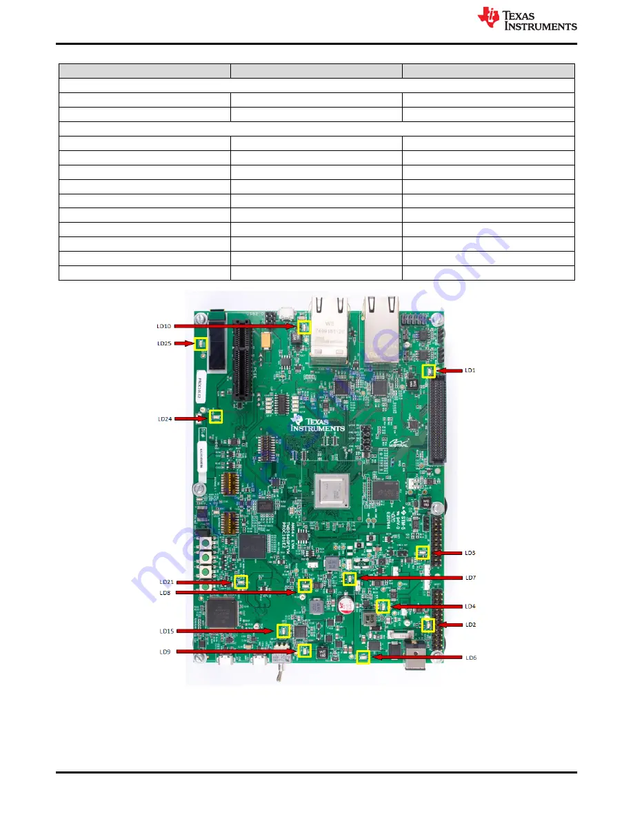
Table 3-5. Power LEDs

Sl.No

Power Supply

LED REF

Before SW1 TURN ON

1

VMAIN

LD6

2

VCC3V3_TA

LD24

After SW1 TURN ON

3

VCC_5V0

LD15

4

VCC3V3_PREREG

LD4

5

VCC_3V3_SYS

LD9

6

VDD_2V5

LD1

7

VDD_1V1

LD10

8

VDDA1V8

LD8

9

VDD_CORE

LD2

10

VCC_CORE

LD7

11

VDD_2V8

LD25

12

VCC1V2_DDR

LD3

Figure 3-6. Power Good LEDs

System Description

www.ti.com

14

AM64x GP EVM User's Guide

SPRUIX0B – FEBRUARY 2021 – REVISED MARCH 2021

Submit Document Feedback

Copyright © 2021 Texas Instruments Incorporated

Summary of Contents for AM64 Series

Page 1: ...ce 26 3 4 8 Memory Interfaces 27 3 4 8 1 DDR4 Interface 27 3 4 8 2 MMC Interface 28 3 4 8 3 OSPI Interface 29 3 4 8 4 SPI EEPROM Interface 30 3 4 8 5 Board ID EEPROM Interface 30 3 4 9 Ethernet Interface 31 3 4 9 1 DP83867 PHY Default Configuration 33 3 4 9 2 DP83869 PHY Default Configuration 33 3 4 9 3 Ethernet LEDs 39 3 4 10 Display Interface 40 3 4 11 USB 2 0 Interface 41 3 4 12 PCIe Interface ...

Page 2: ...art 2 47 Figure 3 29 CAN Interface 48 Figure 3 30 I2C Interfaces and Address Assignment to its Peripherals 51 Figure 3 31 FSI Interface 52 Figure 4 1 AM64x GP EVM Modification Label Location 53 Figure 4 2 XDS110 CCS Connection Error Dialog 54 Figure 4 3 XDS110 debug reset utility command line function 54 List of Tables Table 3 1 Source Clock Selection for the Clock Buffer 10 Table 3 2 VMAIN LED 12...

Page 3: ...nctionality and develop prototypes for a variety of applications The EVM is equipped with a Sitara AM6442 processor along with additional components to allow the user to make use of the various device interfaces including Industrial Ethernet standard Ethernet PCIe Fast Serial Interface FSI and others to easily create prototypes An on board display makes use of AM64x s serial peripheral interface S...

Page 4: ... 3 System Description The following sections describe the AM64x GP EVM design Top down and bottom up views of the PCB are provided in Figure 3 1 and Figure 3 2 for reference to major IC and connector component locations Figure 3 1 Top View of General Processor Board Important Usage Notes www ti com 4 AM64x GP EVM User s Guide SPRUIX0B FEBRUARY 2021 REVISED MARCH 2021 Submit Document Feedback Copyr...

Page 5: ... I2C Boot EEPROM I O Interface One CPSW Gigabit Ethernet port and two Industrial Ethernet ports based on the Gigabit Industrial Communication Subsystem PRU ICSS Gb paired with Texas Instruments Gigabit Ethernet PHY One USB2 0 interface with Micro AB connector Expansion Bus 10051922 1410ELF 14 Pin FPC connector to interface with the OSD9616P0992 10 display High Speed Expansion HSE connector to conn...

Page 6: ... 12V The GP EVM implements a center positive 5 5mm x 2 1mm x 9 5mm Barrel Jack Recommended mating connector CUI In PP3 002AH tuning fork style plug recommended to avoid the possibility of intermittent connections Recommended Power Supply CUI In SDI65 12 UD P5 adapter cords sold separately Example Adapter Cords CUI In AC C7 NA Phihong USA AC15WNA CUI In AC C7 UK Status Output LEDs to indicate power...

Page 7: ...lock diagram of the AM64x GP EVM Figure 3 3 General Processor Board Functional Block Diagram www ti com System Description SPRUIX0B FEBRUARY 2021 REVISED MARCH 2021 Submit Document Feedback AM64x GP EVM User s Guide 7 Copyright 2021 Texas Instruments Incorporated ...

Page 8: ...sible damage to the AM64x GP EVM components the following EVM power on and power off procedures should be utilized 3 3 1 Power On Procedure 1 Place EVM power SW1 switch in OFF position as shown in the figure below 2 Place AM64x boot switch selectors SW2 SW3 into selected boot mode For more details see the bootmode section System Description www ti com 8 AM64x GP EVM User s Guide SPRUIX0B FEBRUARY ...

Page 9: ... LED against reference photo above The following LED should be illuminated LD1 LD2 LD3 LD4 LD6 LD7 LD8 LD9 LD10 LD15 LD24 LD25 3 3 2 Power Off Procedure 1 Switch EVM power switch SW1 to OFF position 2 Disconnect AC power from AC DC converter 3 Remove DC power plug from EVM power jack J6 www ti com System Description SPRUIX0B FEBRUARY 2021 REVISED MARCH 2021 Submit Document Feedback AM64x GP EVM Us...

Page 10: ...vided as per device specific data sheet Table 3 1 Source Clock Selection for the Clock Buffer IN_SEL1 IN_SEL0 Clock Chosen Mount Unmount 0 0 EXT_REFCLK from SoC R40 R45 R248 R253 1 0 Oscillator input R253 R40 R45 R248 Figure 3 4 AM64x GP EVM Clock Tree Note Resistors that are marked with red color box are DNI 3 4 1 2 AM64x SoC Clock Crystal of 25 MHz ABM10W 25 0000MHZ 8 K1Z T3 is provided on EVM a...

Page 11: ...and RESET_REQz Warm reset can also be applied through Test automation header or manual reset switches SW4 SoC and SW6 MCU MCU_PORz input can be applied though switch SW7 The CONN_MCU_RESETz and CONN_MCU_PORz from the safety connector are routed to MCU_RESETz and MCU_PORz respectively thereby providing option for safety connector to create a warm reset and a cold reset as shown in the Figure 3 5 Mo...

Page 12: ...status to indicate VMAIN power good Note The Switch SW1 does not turn of VMAIN It only disables the VCC_5V0 output of LM5140 from which all other power supplies are derived 3 4 3 2 Reverse Polarity Protection A Schottky barrier rectifier with reference D3 is kept for reverse polarity protection which has average forward current IF AV 15 A reverse voltage VR 45 V LD6 status will give power polarity...

Page 13: ...Points Sl No Power Supply Test Point Voltage Top Side 1 VMAIN TP81 12 V 2 VCC_5V0 TP18 5 V 3 VCC3V3_PREREG TP12 3 3 V 4 VCC_3V3_SYS TP44 3 3 V 5 VDD_2V5 TP6 2 5 V 6 VDD_1V1 TP28 1 1 V 7 VDDA1V8 TP29 1 8 V 8 VDD_CORE TP14 0 75 V 9 VCC_CORE TP23 0 75 V 10 VDD_0V85 TP8 0 85 V 11 VDDAR_CORE TP10 0 85 V 12 VCC1V2_DDR TP4 1 2 V 13 VDD_2V8 TP99 2 8 V 14 VCC3V3_TA TP96 3 3 V 15 VDD_1V0 TP56 1 V 16 VPP_DDR...

Page 14: ...3_PREREG LD4 5 VCC_3V3_SYS LD9 6 VDD_2V5 LD1 7 VDD_1V1 LD10 8 VDDA1V8 LD8 9 VDD_CORE LD2 10 VCC_CORE LD7 11 VDD_2V8 LD25 12 VCC1V2_DDR LD3 Figure 3 6 Power Good LEDs System Description www ti com 14 AM64x GP EVM User s Guide SPRUIX0B FEBRUARY 2021 REVISED MARCH 2021 Submit Document Feedback Copyright 2021 Texas Instruments Incorporated ...

Page 15: ... sequence of all the Power supplies present on the EVM Board Figure 3 7 Power ON and OFF Sequencing www ti com System Description SPRUIX0B FEBRUARY 2021 REVISED MARCH 2021 Submit Document Feedback AM64x GP EVM User s Guide 15 Copyright 2021 Texas Instruments Incorporated ...

Page 16: ...re and SoC Array Core and other Array Core Voltages and based requirement This can be configured by the placement of resistors as mentioned in Figure 3 8 Figure 3 8 Core Supply and Array Core Supply Options The SoC has different IO groups Each IO group is powered by specific power supplies as shown in Table 3 6 Table 3 6 SoC Power Supply SI No Power Supply SoC Supply Rails IO Power Group Power 1 V...

Page 17: ...switch capable of connecting to a strong pull up resistor Switch set to ON corresponds to logic HIGH while OFF corresponds to logic LOW For a full description of all AM64x SoC supported bootmodes see the AM64x Sitara Processors Data Manual and AM64x Processors Silicon Revision 1 0 Texas Instruments Families of Products Technical Reference Manual The following boot modes are supported by EVM 1 OSPI...

Page 18: ...provide means to select the boot mode before the device is powered up They are divided into the following categories Note The following bitpattern is reversed in the table from the switch order System Description www ti com 18 AM64x GP EVM User s Guide SPRUIX0B FEBRUARY 2021 REVISED MARCH 2021 Submit Document Feedback Copyright 2021 Texas Instruments Incorporated ...

Page 19: ... slow speed backup BOOTMODE 6 3 This provides primary boot mode configuration to select the requested boot mode after POR that is the peripheral memory to boot from Table 3 9 Boot Device Selection BOOTMODE 6 3 SW2 7 SW2 6 SW2 5 SW2 4 Primary Boot Device Selected off off off off Reserved off off on on OSPI off off on off QSPI off off on on SPI off on off off Reserved off on off on Reserved off on o...

Page 20: ...o boot from if primary boot device failed Table 3 11 Backup Boot Mode Selection BOOTMODE 12 10 SW3 2 SW3 1 SW2 8 Backup Boot Device Selected off off off None No backup mode off off on USB off on off Reserved off on on UART on off off Reserved on off on MMC SD on on off SPI on on on I2C BOOTMODE 13 These pins provide optional settings and are used in conjunction with the backup boot device devices ...

Page 21: ...ese signals to the HSE or Trace connector as mentioned in the Table 3 13 The pinout of TI20 pin connector and MIPI60 pin connector are given in Table 3 13 and Table 3 15 respectively Table 3 13 Selection of HSE Connector and JTAG TRACE Functionality Signals Selected Mount Un Mount HSE Connector default RA1 RA2 RA3 RA4 RA5 RA6 R390 R391 R393 R392 JTAG Trace signals to J33 RA2 RA1 RA4 RA3 RA6 RA5 R3...

Page 22: ... NC 3 JTAG_MIPI_TCK 33 MIPI_TRC_DAT07 4 MIPI_TDO_R 34 NC 5 MIPI_TDI_R 35 MIPI_TRC_DAT08 6 MIPI_EMU_RSTn 36 NC 7 MIPI_RTCK 37 MIPI_TRC_DAT09 8 MIPI_TRST _R 38 JTAG_MIPI_EMU0 System Description www ti com 22 AM64x GP EVM User s Guide SPRUIX0B FEBRUARY 2021 REVISED MARCH 2021 Submit Document Feedback Copyright 2021 Texas Instruments Incorporated ...

Page 23: ...automation header includes four GPIOs two I2C interfaces The basic controls as follows Table 3 16 List of Signals Routed to Test Automation Header Signal Signal Type Function POWER_DOWN GPIO Instructs the EVM to power down all circuits POR GPIO Creates a PORz into the AM64x SoC WARM_RESET GPIO Creates a RESETz into the AM64x SoC GPIO1 GPIO GPIO for communication with AM64x SoC GPIO2 GPIO Connected...

Page 24: ...surements of customer applications Note The power measurements are not a substitute for the AM64x Power Estimation Tool and should not be used for the design of power supply solutions Power measurements will vary based on silicon process and environment and measurements should only be used for comparison with other measurements taken on the same EVM Figure 3 12 Test Automation Header System Descri...

Page 25: ...D Ground 26 TEST_POWERDOWN Input 27 TEST_PORz Input 28 TEST_WARMRESETn Input 29 NC NA 30 TEST_GPIO1 Bidirectional 31 TEST_GPIO2 Bidirectional 32 TEST_GPIO3 Input 33 TEST_GPIO4 Input 34 DGND Ground 35 NC NA 36 SOC_I2C1_SCL Bidirectional 37 BOOTMODE_I2C_SCL Bidirectional 38 SOC_I2C1_SDA Bidirectional 39 BOOTMODE_I2C_SDA Bidirectional 40 DGND Ground 41 DGND Ground 42 DGND Ground www ti com System Des...

Page 26: ...32H htm The FT_Prog has three modes of operation Idle Mode Program Mode and Edit Mode FT_Prog programming parameters can be saved in files referred as EEPROM templates Once defined these EEPROM templates can be loaded by FT_Prog and used to program EEPROMs Idle Mode is the initial mode of operation when the program is launched Edit Mode is used to edit the settings of an EEPROM template Program Mo...

Page 27: ... make one x16 The DDR memory is mounted on board single chip The placement and routing of the DDR4 device will be point to point with VTT termination The DDR4 requires 1 2V and thus reduces power demand Figure 3 14 DDR4 Interface www ti com System Description SPRUIX0B FEBRUARY 2021 REVISED MARCH 2021 Submit Document Feedback AM64x GP EVM User s Guide 27 Copyright 2021 Texas Instruments Incorporate...

Page 28: ...t to generate the uSD voltage based on IO level negotiation with the uSD card For high speed cards ROM code of the SoC attempts to find the fastest speed that the card and controller can support and can have a transition to 1 8V The internal SDIO LDO output from the SoC is provided on the CAP_VDDSHV_SDLDO pin CAP_VDDSHV_SDLDO is connected to both the IO voltage of SD signals and VDDSHV_MMC1 power ...

Page 29: ...BCLK from SoC Mount R600 R591 and DNI R601 R592 Note For more information see the OSPI and QSPI Board Design and Layout Guidelines section in the AM64x Sitara Processors Data Manual OSPI QSPI implementation 0 ohm resistors are provided for DATA 7 0 DQS INT and CLK signals Footprints to mount external pull up resistors are provided on DATA 7 0 to prevent bus floating The footprint for the OSPI memo...

Page 30: ... memory are preprogrammed with identification information for each board The remaining 32509 bytes are available to the user for data or code storage Table 3 18 Board ID Memory Header Information Header Field Name Size bytes Comments EE3355AA MAGIC 4 Magic Number TYPE 1 Fixed length and variable position board ID header 2 Size of payload BRD_INFO TYPE 1 payload type Length 2 offset to next header ...

Page 31: ... also multiplexed with PRG0 signals a mux is needed to select the path from the SoC to this PHY in CPSW mode or to the HSE connector PRG0 mode The selection is done using a GPIO from the 24 bit IO expander The second PHY connected to stacked RJ45 connector J21B is interfaced to the PRG1_RGMII2 port of the SoC This port is directly multiplexed with the CPSW_RGMII2 port In order to select between CP...

Page 32: ...hat it should support both RGMII and MII modes without the use of CRS and COL signals as they are multiplexed with the CPSW_RGMII1 used for the first PHY Hence the same DP83869 48pin PHY is used for this port as well Figure 3 19 Ethernet Interface ICSSG Domain System Description www ti com 32 AM64x GP EVM User s Guide SPRUIX0B FEBRUARY 2021 REVISED MARCH 2021 Submit Document Feedback Copyright 202...

Page 33: ...sistor strapping generates four distinct voltages ranges The resistors are connected to the RX data pins which are normally driven by the PHY and are inputs to the AM64x The voltage range for each mode is shown below Mode 0 0 V to 0 3069 V Mode 1 0 4488 V to 0 6072 V Mode 2 0 7227 V to 0 924 V Mode 3 1 98 V to 2 9304 V The two level strap pins based on resistor strapping generates two distinct vol...

Page 34: ... PHY_AD2 3 1 3 1 RX_D0 PHY_AD1 0 0 3 1 ICSSG2PHY Address 01111 PHY_AD0 0 0 3 1 Modes of Operation RX_CNTL Mirror Enable 0 0 0 0 Mirror Enable Disabled LED_2 ANEGSEL_1 0 0 0 0 Auto negotiation 10 100 1000 advertised Auto MDI X LED_1 ANEGSEL_0 0 0 0 0 LED_0 ANEG_DIS 0 0 0 0 JTAG_TDO GPIO_1 OPMODE_0 0 0 0 0 RGMII to Copper 1000BaseT 100Base TX 10Base Te The PHY devices include integrated MDI terminat...

Page 35: ...s having internal pulldown resistor to set RGMII TX Clock Skew in the DP83867 device and to select Auto Negotiation mode in the DP83869 device The default condition is to auto negotiate and advertise link as 10 100 1000Mbps this can be changed using the strap resistors provided The pull up resistor used for strap setting results in dim LED lighting when LED is driven directly So a MOSFET is used t...

Page 36: ...ernet Interface CPSW Ethernet Strap Settings System Description www ti com 36 AM64x GP EVM User s Guide SPRUIX0B FEBRUARY 2021 REVISED MARCH 2021 Submit Document Feedback Copyright 2021 Texas Instruments Incorporated ...

Page 37: ...rnet Interface ICSSG1 Ethernet Strap Settings www ti com System Description SPRUIX0B FEBRUARY 2021 REVISED MARCH 2021 Submit Document Feedback AM64x GP EVM User s Guide 37 Copyright 2021 Texas Instruments Incorporated ...

Page 38: ... Settings Note Resistors that are highlighted by red color box are DNI components System Description www ti com 38 AM64x GP EVM User s Guide SPRUIX0B FEBRUARY 2021 REVISED MARCH 2021 Submit Document Feedback Copyright 2021 Texas Instruments Incorporated ...

Page 39: ...itionally there are eight LED s that are connected to an IO Expander which is controlled by the SoC via the I2C1 port These eight LED s can be toggled based on the user application Figure 3 23 GP Board Ethernet Interface LEDs www ti com System Description SPRUIX0B FEBRUARY 2021 REVISED MARCH 2021 Submit Document Feedback AM64x GP EVM User s Guide 39 Copyright 2021 Texas Instruments Incorporated ...

Page 40: ...5 mm The Display is connected to the 14 Pin FPC connector on the AM64x EVM having part number 10051922 1410ELF from Amphenol ICC and the pin details are mentioned in Table 3 21 Table 3 21 Display Connector J36 Pin Out Pin No Signal 1 C2P 2 C2N 3 C1P 4 C1N 5 VDDB 6 NC 7 VSS 8 VDD 9 RES 10 SCL 11 SDA 12 IREF 13 VCOMH 14 VCC System Description www ti com 40 AM64x GP EVM User s Guide SPRUIX0B FEBRUARY...

Page 41: ...ration or endpoint operation with a cross over cable SoC_I2C1 is used for control purpose The link activation signal from PCIe connectors is pulled up to VCC3V3_SYS Clock SERDES REFCLK is routed to the PCIe REF CLK pins to allow either receiving or providing a clock from the connector no separate PLL to generate PCIe REF CLK available on the EVM Hot plug The PRSNT1 and PRSNT2 signals are the hot p...

Page 42: ...12V VDD_12V 4 GND GROUND GND GROUND 5 JTAG2 TP SMCLK SoC_I2C1_CLK 6 JTAG3 TP SMDATA SoC_I2C1_SDA 7 JTAG4 TP GND GROUND 8 JTAG5 TP 3V3 VCC3V3_SYS 9 3V3 VCC3V3_SYS JTAG1 TP 10 3V3 VCC3V3_SYS 3V3 VAUX VCC3V3_SYS 11 PERST J24 2 WAKE Pulled up to VCC3V3_SYS 12 GND GROUND RSVD4 Pulled up to VCC3V3_SYS 13 REFCLK SERDES_REFCLK0P GND GROUND 14 REFCLK SERDER_REFCLK0N PETp0 SERDES_TXP0 15 GND GROUND PETn0 SE...

Page 43: ...hese signals are muxed so that they are available to both the FSI connector and the expansion connector FSI_TX0 signals and FSI_RX0 signals are connected to the mux The mux is controlled by jumper The default state drives the signals from AM64x SoC to the HSE connector unless the jumper is installed The boards will be delivered with the jumper installed Additional signals like UART4 I2C0 SPI1 and ...

Page 44: ...CLK D1 SOC_SPI1_CS0 C2 VCC1V8_HSE D2 SOC_SPI1_CS1 C3 VCC1V8_HSE D3 MCU_RESETZ C4 DGND D4 DGND C5 PRG0_PRU0GPO13 D5 PRG0_PRU1GPO13 C6 PRG0_PRU0GPO5 D6 PRG0_PRU1GPO5 C7 DGND D7 DGND C8 PRG0_PRU1GPO3 D8 PRG0_PRU0GPO6 C9 PRG0_PRU0GPO14 D9 PRG0_PRU1GPO2 C10 DGND D10 DGND C11 PRG0_PRU1GPO15 D11 PRG0_PRU1GPO11 C12 PRG1_PRU1GPO19 D12 PRG0_PRU0GPO15 C13 DGND D13 DGND C14 GPMC0_AD2 D14 GPMC0_AD1 C15 GPMC0_A...

Page 45: ...SE_DETECT E19 GPMC0_CSN1 E5 DGND E20 DGND E6 DGND E21 GPMC0_AD11 E7 DGND E22 DGND E8 PRG0_PRU0GPO1 E23 HSE_PRG0_PRU1_GPO9 E9 PRG0_PRU0GPO16 E24 HSE_MCAN0_RX UART4_TXD E10 DGND E25 DGND E11 PRG0_PRU1GPO6 E26 HSE_GPIO0_38 E12 PRG0_PRU1GPO14 E27 HSE_PRG0_PRU1_GPO10 E13 PRG1_PRU1GPO18 E28 DGND E14 GPMC0_AD0 E29 DGND E15 GPMC0_AD3 E30 MCU_PORZ Figure 3 26 High Speed Expansion Connector www ti com Syste...

Page 46: ...7 High Speed Expansion Connector Part 1 System Description www ti com 46 AM64x GP EVM User s Guide SPRUIX0B FEBRUARY 2021 REVISED MARCH 2021 Submit Document Feedback Copyright 2021 Texas Instruments Incorporated ...

Page 47: ... TCAN1042HGV RXD and TXD pins are connected to MCAN0_RX UART4_TXD and MCAN0_TX UART4_RXD pins of AM64x respectively STB pin of the IC is by default connected to ground to avoid IC entering stand by mode The STB pin is controlled by GPIO to enable Standby mode The pin out of CAN connector is shown in Table 3 25 Table 3 25 CAN J31 and J32 Pin out CAN0 J31 CAN1 J32 Pin No Signal Pin No Signal 1 MCAN0...

Page 48: ... be applied though switch SW7 3 4 16 ADC Interface A 20 pin connector J3 of part number TSW 110 07 S D for connecting ADC signals of AM64x SoC The connector includes ADC0_AIN0 7 VDDA_ADC connections and ground connections Table 3 26 ADC Connector J3 Pin out Pin No Signal Pin No Signal 1 DGND 11 ADC0_AIN7 2 NC 12 DGND 3 ADC0_AIN6 13 DGND 4 VDDA_ADC 14 ADC0_AIN1 5 DGND 15 ADC0_AIN0 6 ADC0_AIN2 16 DG...

Page 49: ...4 CONN_MCU_PORZ 3 4 18 SPI Interface SPI0 A 1Kbit SPI EEPROM 93LC46B is interfaced to SPI0 port of AM64x processor It is used for testing purposes SPI1 This interface is routed to the HSE Connector The SPI1 interface signals are at a 3 3V IO level SPI1_CS0 is routed to the HSE expansion header J2 SPI1_CS1 is routed to the HSE expansion header J2 3 4 19 I2C Interface There are five I2C interfaces u...

Page 50: ...nnected to a test header J4 for AM64x processor slave operation Pin outs of I2C test header is given in Table 3 29 Table 3 29 I2C Test Header J4 Pin out Pin No Signal 1 SoC_I2C1_SCL 2 SoC_I2C0_SDA 3 DGND 4 INA_ALERT 5 NC 3 MAIN_I2C3 This is connected to the expansion board connector from a mux I2C3 is muxed with the MCAN signals The default state of the mux is MCAN 4 MCU_I2C0 This is connected to ...

Page 51: ...ure 3 30 I2C Interfaces and Address Assignment to its Peripherals www ti com System Description SPRUIX0B FEBRUARY 2021 REVISED MARCH 2021 Submit Document Feedback AM64x GP EVM User s Guide 51 Copyright 2021 Texas Instruments Incorporated ...

Page 52: ...lled by GPIO from IO Expander A logic low in Mux select pin connects port A and Port B1 whereas a logic high connects A port to B2 port The default state of mux drives the signals from A port to B1 port which is connected to HSE connector Table 3 30 FSI J5 Connector Pin out Pin No Signal 1 FSI_TX0_CLK 2 FSI_RX0_CLK 3 DGND 4 DGND 5 FSI_TX0_D0 6 FSI_RX0_D0 7 FSI_TX0_D1 8 FSI_RX0_D1 9 DGND 10 VCC_3V3...

Page 53: ...e 4 1 AM64x GP EVM Modification Label Location 4 1 Issue 1 Embedded XDS110 Connection to AM64x Target in CCS Applicable EVM Revisions E2 Issue Description On some EVM the embedded XDS110 U59 has been shown to fail initial target connection to AM64x target in CCS after first EVM and XDS110 power cycle No problem exists when using an attached external emulator over the CTI20 header J25 This failure ...

Page 54: ...e TRSTSN through the XDS110 debug command line utility xds110reset found in the CCS XDS110 utility directory In the Windows OS installation for a default installation of CCS version 10 11 this tool is found in the directory C ti ccs1011 ccs ccs_base common uscif xds110 This command can be executed on the Windows command prompt terminal when the embedded XDS110 is powered on and connected to the ho...

Page 55: ...fication 5 description All components located on the bottom of the PCB assembly layer Remove U78 Short U78 2 to U78 4 Short U78 8 to U78 6 5 References AM64x Sitara Processors Data Manual AM64x Processors Silicon Revision 1 0 Texas Instruments Families of Products Technical Reference Manual 6 Revision History NOTE Page numbers for previous revisions may differ from page numbers in the current vers...

Page 56: ...s are subject to change without notice TI grants you permission to use these resources only for development of an application that uses the TI products described in the resource Other reproduction and display of these resources is prohibited No license is granted to any other TI intellectual property right or to any third party intellectual property right TI disclaims responsibility for and you wi...

Reviews: