background image

BP-ADS7128 EVM Initial Setup

www.ti.com

16

SBAU331 – May 2019

Submit Documentation Feedback

Copyright © 2019, Texas Instruments Incorporated

BP-ADS7128 BoosterPack™ Plug-In Module

3.3.2.2.5

Average and Statistics Configuration

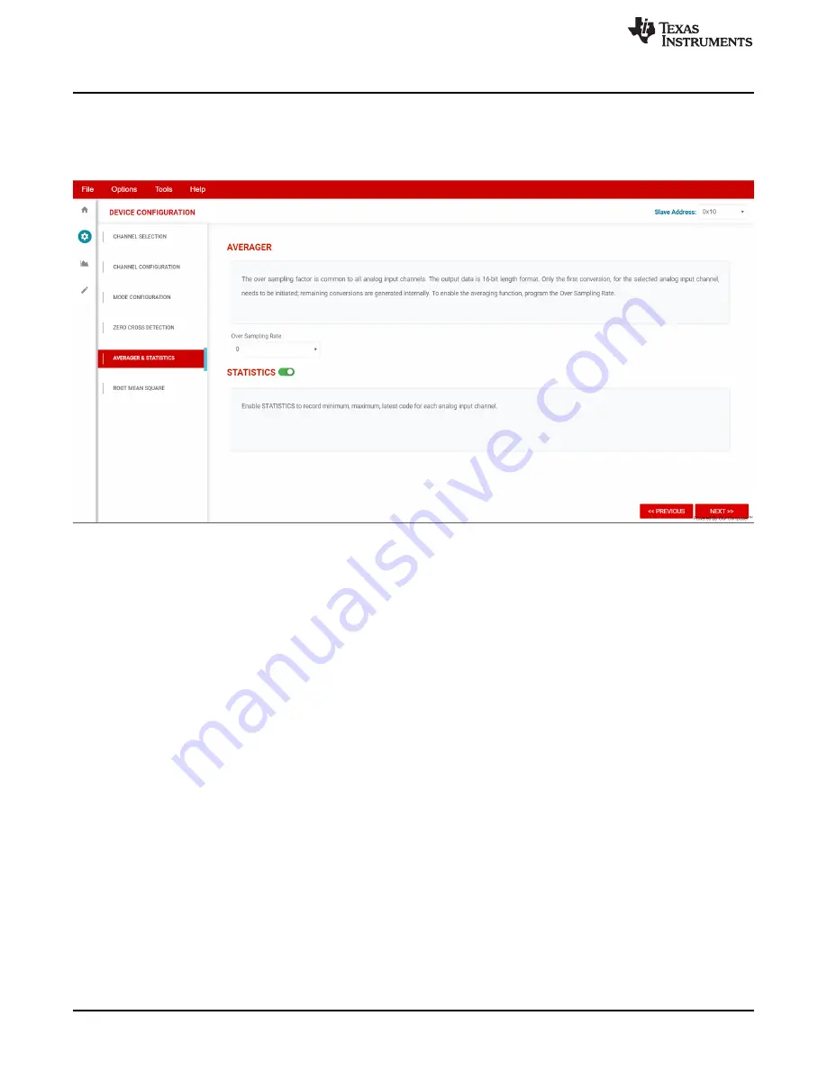
Within the averager and statistics page, as shown in

Figure 16

the oversampling ratio can be selected

that applies to all analog input channels enabled. The statistic function can also be enabled or disable
within this page.

Figure 16. Averager and Statistics Page

Summary of Contents for ADS7028

Page 1: ...28EVM Block Diagram 3 2 BP ADS7128 Top Level Overview 4 3 Browser Extension and TI Cloud Agent Installation 6 4 MSP432E401Y LaunchPad 5V OTG Jumper 7 5 LaunchPad Debug Port 8 6 UNIFLASH Programming Set Up 8 7 FLASH Programming LaunchPad 9 8 Successful FLASH Program 9 9 BP ADS7128 Stacked on the MSP432E401Y LaunchPad 10 10 ADS7128 GUI Landing Page 11 11 ADS7128 Device Configuration Tab 12 12 Channe...

Page 2: ...le 29 BP ADS7128 Power Plane Layer 29 30 ADS7128 BoosterPack Schematic Diagram 30 List of Tables 1 Channel Connections 5 2 Bill of Materials 25 Trademarks BoosterPack LaunchPad are trademarks of Texas Instruments Chrome is a trademark of Google Firefox is a trademark of Mozilla All other trademarks are the property of their respective owners ...

Page 3: ...s controlled by commands received from the ADS7128 GUI and returns data to the GUI for display and analysis If the MSP EXP432E401Y is not used the BoosterPack plug in module format of the BP ADS7128 board allows for an alternative external host to communicate with the ADS7128 The BP ADS7128 incorporates all required circuitry and components with the following features ADS7128 low power ultra small...

Page 4: ...BP ADS7128 BoosterPack Plug In Module 2 BP ADS7128EVM Overview This section describes various onboard components that are used to interface the analog input general purpose inputs outputs GPIOs digital interface and provide power supply to the BP ADS7128 Figure 2 shows a BP ADS7128 overview Figure 2 BP ADS7128 Top Level Overview ...

Page 5: ... GPIO for channel 5 of the ADC J5 11 Single ended analog input or GPIO for channel 6 of the ADC J5 12 Single ended analog input or LED GPIO for channel 7 of the ADC J5 3 and J5 4 J5 9 and J5 10 BoosterPack ground 2 2 Digital Interface As noted in Section 1 the BP ADS7128 interfaces with the MSP EXP432E401Y LaunchPad which in turn communicates with the computer over the USB The two devices on the b...

Page 6: ...are installation 1 On the BP ADS7128 BoosterPack plug in module site click on the link under Software to connect to the installer Connecting to the installer may require you to login to your user account privileges to use the online version and to install the available applications 2 Click on the BP ADS7128 GUI icon As shown in Figure 3 first time users may be prompted to download and install the ...

Page 7: ... ships with a default firmware program flashed on its memory When a LaunchPad is connected to the PC for the first time its firmware must be updated for communications with the BP ADS7128 The following steps describe how to program this firmware on the flash memory 1 On the MSP432E401Y LaunchPad remove jumper JP6 from its default position and place this jumper on the JP1 jumper as shown in Figure ...

Page 8: ...Y LaunchPad debug port connector as shown in Figure 5 to an available USB port on the PC Figure 5 LaunchPad Debug Port 3 As shown in Figure 6 after the BP ADS7128 GUI has been set up select Program Device from the File menu option This selection automatically recognizes the MSP432E401Y LaunchPad and FLASH program see Figure 7 to communicate with the BP ADS7128 Figure 6 UNIFLASH Programming Set Up ...

Page 9: ...back Copyright 2019 Texas Instruments Incorporated BP ADS7128 BoosterPack Plug In Module Figure 7 FLASH Programming LaunchPad 4 After programming and verification is successful as shown in Figure 8 disconnect the USB from the MSP EXP432E401Y debug port Figure 8 Successful FLASH Program ...

Page 10: ...DS7128 on the MSP432E401Y LaunchPad MSP EXP432E401Y Make sure the 20 pin connector J1 J3 on the BP ADS7128 is mapped to connector J5 J7 and that connector J4 J2 on the BP ADS7128 is mapped to connector J8 J6 on the MSP EXP432E401Y The silk screen on the BP ADS7128 must match with the MSP EXP432E401Y 2 Connect the MSP EXP432E401Y micro USB data port to an available USB port on the PC Figure 9 shows...

Page 11: ...the ADS7128 device The left corner shows the tabs to navigate through the GUI home function configurations data capture and register map When the BP ADS7128 is stacked on the MSP432E401Y and connected to the PC via the micro USB cable the GUI detects the BoosterPack module by reading the onboard EEPROM When detected and connected the GUI indicates this status as connected At the bottom left corner...

Page 12: ... to navigate through the various functions of the ADS7128 The right most section displays the configuration options for each function Figure 11 ADS7128 Device Configuration Tab 3 3 2 1 Channel Selection This page selects channels and functionality Each channel can be enabled or disabled and configured as an analog input default digital input or digital output On the top right corner is an option t...

Page 13: ...gital input and digital output respectively The Channel Configuration page then automatically updates to reflect the selected channel options 3 3 2 2 1 Input Channels Continuing with the example both analog and digital inputs are displayed as shown in Figure 12 in the Input Channels tab Analog channels are listed on top digital channels are listed below The available configuration options are disp...

Page 14: ...ternal host processor to directly request and control when the data are sampled The host provides I2 C frames to control conversions and the captured data are returned over the I2 C bus after each conversion Auto Sequence Mode The host can configure the device to scan through the enabled analog input channels The host must provide continuous clocks SCL to the device to scan through the channels an...

Page 15: ...ure 14 Sampling Mode Configuration 3 3 2 2 4 Zero Cross Detection ZCD The zero cross detection tab as shown in Figure 15 provides a timing diagram demonstrating the ZCD functionality and the blanking time transients of the input signal only one input channel can be selected to monitor The programmable blanking time can be disabled or enabled Figure 15 Zero Cross Detection Page ...

Page 16: ...DS7128 BoosterPack Plug In Module 3 3 2 2 5 Average and Statistics Configuration Within the averager and statistics page as shown in Figure 16 the oversampling ratio can be selected that applies to all analog input channels enabled The statistic function can also be enabled or disable within this page Figure 16 Averager and Statistics Page ...

Page 17: ...orated BP ADS7128 BoosterPack Plug In Module 3 3 2 2 6 Root Mean Square The root mean square RMS page as shown in Figure 17 displays the equation that the device uses to calculate the root mean square if enabled Based on the number of samples selected the RMS is calculated using the final formula shown Figure 17 ADS7128 RMS Page ...

Page 18: ... results of the sampled data of the enabled channels As shown in Figure 18 clicking the red Capture button commences a sample data set This tab features two pages Analog Inputs The sample and conversion results for each enabled analog input is displayed in this page Digital I O The enabled digital channels input or output are displayed in this page See Section 3 3 5 for more information on capturi...

Page 19: ... to read registers individually read all the registers at the same time or write an individual register Users can choose to have the register values modified in the GUI to be written on the device instantaneously by selecting the Immediate option or later using the Deferred option In the field view the registers are broken down into the configurable bits they are made up of When making changes the...

Page 20: ...input page provides an interface to the conversion results for analog input channels Data are captured as shown in Figure 20 by clicking on the Capture Data button The analog inputs page also displays Number of samples per the enabled analog input channels A drop down option for increasing the oversampling rate A drop down option for selecting input channel display Displays the minimum and maximum...

Page 21: ...g input conversion results at a time in auto sequence mode all sampled channels are displayed As shown in Figure 21 select the channel through the drop down menu shown Figure 21 Time Domain Channel Selection Within the time domain graph the high and low thresholds configured in Section 3 3 2 2 are automatically displayed inFigure 22 as solid red to visually demonstrate the levels that the analog s...

Page 22: ...k Plug In Module 3 3 5 1 2 Histogram Graph Display The conversion results can also be shown as a histogram through the histogram tab shown in Figure 23 within the analog input data capture The high and low threshold levels and the configured hysteresis are also displayed in the histogram graph Figure 23 Histogram Graph Display With Threshold and Hysteresis ...

Page 23: ...rm As shown in Figure 24 if an analog input signal crosses the configured thresholds then an alarm is triggered as demonstrated in the analog inputs page within the data capture tab This page provides an ALARM section where the corresponding image to the threshold crossed high or low turns red when triggered The alarm can be cleared by clicking on the red icon Figure 24 Alarm Triggered ...

Page 24: ...e for a state change rising edge of falling edge The icon turns red when triggered Figure 25 Digital I O Page Display 4 Input Signal Conditioning Block on the BP ADS7128 For applications where the input signal requires additional conditioning before being interfaced to the ADC the BP ADS7128 has an onboard signal conditioning path on channel 0 between the input signal and the ADS7128 By default th...

Page 25: ...AAN Sullins Connector Solutions J5 1 Header 100mil 6x2 Tin TH PEC06DAAN Sullins Connector Solutions R2 1 RES 1 69 M 1 0 063 W AEC Q200 Grade 0 0402 CRCW04021M69FKED Vishay Dale R3 R26 2 RES 1 00 M 1 0 1 W 0402 ERJ 2RKF1004X Panasonic R4 1 RES 0 5 0 063 W 0402 RC0402JR 070RL Yageo America R5 R6 R7 3 RES 1 00 k 1 0 063 W 0402 MCR01MZPF1001 Rohm R8 R9 R12 R14 R15 R18 R20 R23 8 RES 10 0 k 1 0 063 W 04...

Page 26: ... ti com 26 SBAU331 May 2019 Submit Documentation Feedback Copyright 2019 Texas Instruments Incorporated BP ADS7128 BoosterPack Plug In Module 5 2 PCB Layout Figure 26 Figure 27 Figure 28 and Figure 29 illustrate the EVM PCB layout Figure 26 BP_ADS7128 PCB Top Overlay ...

Page 27: ...Printed Circuit Board Layout and Schematics 27 SBAU331 May 2019 Submit Documentation Feedback Copyright 2019 Texas Instruments Incorporated BP ADS7128 BoosterPack Plug In Module Figure 27 BP ADS7128 Top Layer Copper and Silkscreen ...

Page 28: ...uit Board Layout and Schematics www ti com 28 SBAU331 May 2019 Submit Documentation Feedback Copyright 2019 Texas Instruments Incorporated BP ADS7128 BoosterPack Plug In Module Figure 28 BP ADS7128 Bottom Layer Copper and Silkscreen ...

Page 29: ...and Schematics 29 SBAU331 May 2019 Submit Documentation Feedback Copyright 2019 Texas Instruments Incorporated BP ADS7128 BoosterPack Plug In Module Figure 29 BP ADS7128 Power Plane Layer 5 3 Schematics Figure 30 illustrates the ADS7128 BoosterPack schematics ...

Page 30: ...Circuit Board Layout and Schematics www ti com 30 SBAU331 May 2019 Submit Documentation Feedback Copyright 2019 Texas Instruments Incorporated BP ADS7128 BoosterPack Plug In Module Figure 30 ADS7128 BoosterPack Schematic Diagram ...

Page 31: ...se resources are subject to change without notice TI grants you permission to use these resources only for development of an application that uses the TI products described in the resource Other reproduction and display of these resources is prohibited No license is granted to any other TI intellectual property right or to any third party intellectual property right TI disclaims responsibility for...

Reviews: