background image

2-4-1

U29PHSDA

DISASSEMBLY/ASSEMBLY PROCEDURES

OF DECK MECHANISM

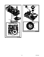
Before following the procedures described below, be sure to remove the deck assembly from the cabinet. (Refer to
CABINET DISASSEMBLY INSTRUCTIONS.)
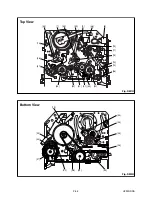
All the following procedures, including those for adjustment and replacement of parts, should be done in Eject
mode; see the positions of [44] and [45] in Fig. DM1H on page 2-4-3. When reassembling, follow the steps in
reverse order.

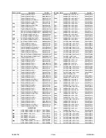
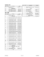
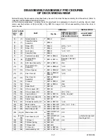
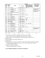
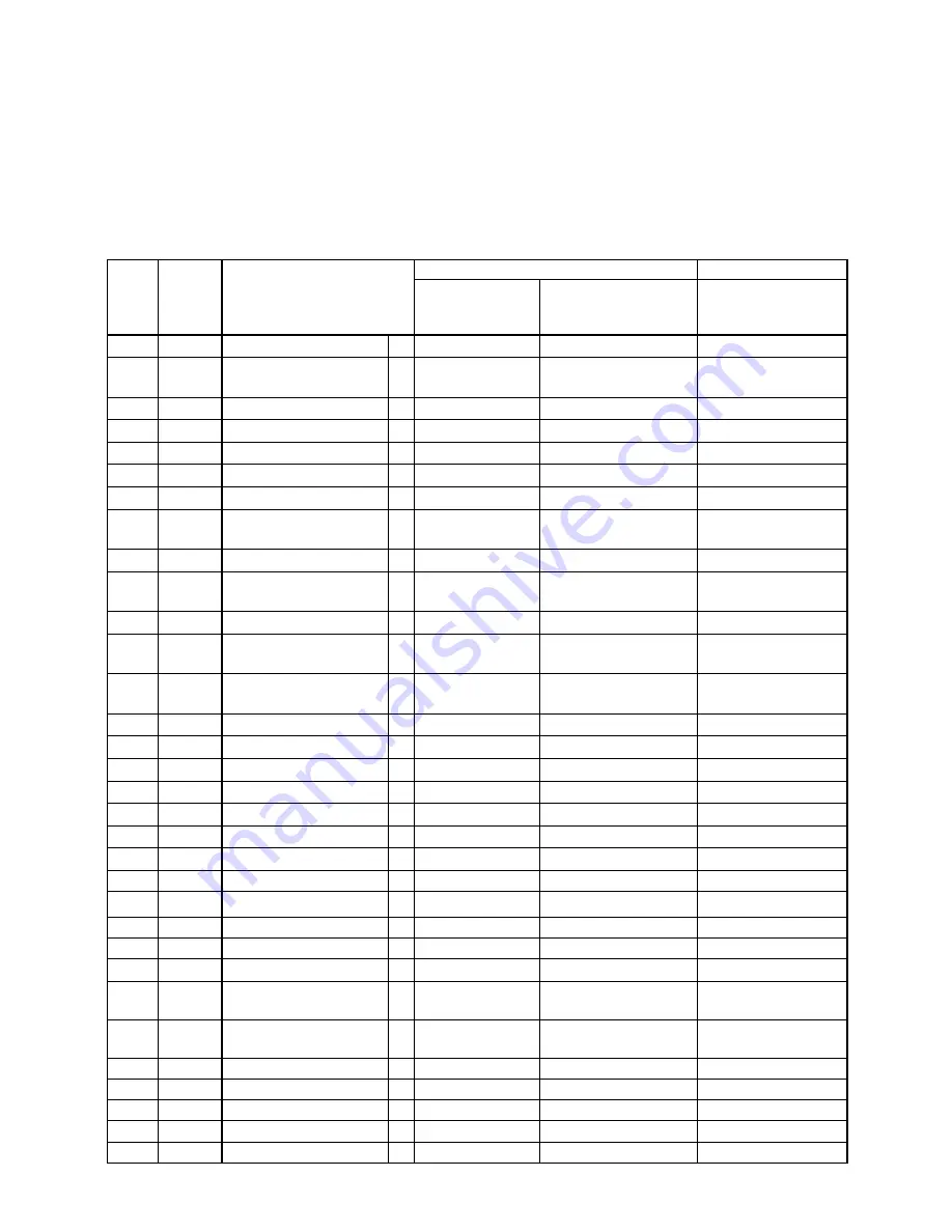
STEP
/LOC.

No.

START-

ING

No.

PART

REMOVAL

INSTALLATION

Fig. No.

REMOVE/*UNHOOK/
UNLOCK/RELEASE/
UNPLUG/DESOLDER

ADJUSTMENT

CONDITION

[1]

[1]

Guide Holder A

T

DM3H

2(S-1)

[2]

[1]

Cassette Holder 
Assembly

T

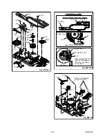
DM4H

[3]

[2]

Slider (SP)

T

DM5H

(S-1A), *(L-1)

[4]

[2]

Slider (TU)

T

DM5H

*(L-2)

[5]

[4]

Lock Lever

T

DM5H

*(L-3), *(P-1)

[6]

[2]

Cassette Plate

T

DM5H

[7]

[7]

Cylinder Assembly

T

DM1H, DM6H

Desolder, 3(S-2)

[8]

[8]

Loading Motor 
Assembly

T

DM1H,  DM7H

Desolder, LDG Belt, 
2(S-3)

[9]

[9]

ACE Head Assembly

T

DM1H, DM7H

(S-4)

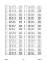
[10]

[2]

Tape Guide Arm 
Assembly

T

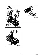
DM1H, DM8H-1

*(P-2)

[11]

[10]

C Door Opener 

T

DM1H, DM8H-1

(S-4A), *(L-4)

[12]

[11]

Pinch Arm (B)

T

DM1H, DM8H-1, 
DM8H-2

*(P-3)

[13]

[12]

Pinch Arm (A) 
Assembly

T

DM1H, DM8H-1, 
DM8H-2

[14]

[14]

FE Head

T

DM1H, DM9H

(S-5)

[15]

[15]

Prism

T

DM1H, DM9H

(S-6)

[16]

[2]

Slider Shaft

T

DM10H

*(L-5)

[17]

[16]

C Drive Lever (SP)

T

DM10H

[18]

[16]

C Drive Lever (TU)

T

DM10H

(S-7), *(P-4)

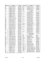
[19]

[19]

Capstan Motor

B

DM2H, DM11H

3(S-8), Cap Belt

[20]

[20]

Clutch Assembly (HI)

B

DM2H, DM12H

(C-1)

[21]

[20]

Center Gear

B

DM12H

*

[22]

[22]

F Brake Assembly (HI)

B

DM2H, DM12H

*(L-6)

[23]

[22]

Worm Holder

B

DM2H, DM13H-1

(S-9), *(L-7), *(L-8)

[24]

[22]

Pulley Assembly (HI)

B

DM2H, DM13H-1

[25]

[25]

Mode Gear (LM)

B

DM2H, DM13H-1

(C-2)

[26]

[20],[25]

Mode Lever (HI)

B

DM2H, DM13H-1, 
DM13H-2

(C-3)

[27]

[22],[23],

[26]

Cam Gear (A) (HI)

B

DM2H, DM13H-1, 
DM13H-2

(C-4)

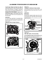
(+)Refer to Alignment 
Sec.Page 2-5-1

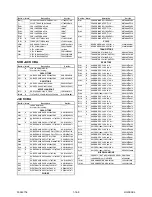
[28]

[26]

TR Gear C

B

DM2H, DM13H-1

(C-5)

[29]

[28]

TR Gear Spring

B

DM13H-1

[30]

[29]

TR Gear A/B

B

DM13H-1

[31]

[31]

FF Arm (HI)

B

DM1H, DM14H

[32]

[26]

Idler Assembly (HI)

B

DM1H, DM14H

*(L-9)

Summary of Contents for TVCR-210

Page 1: ...reparation for Servicing I Adjustment Procedures I Schematic Diagrams I CBA s I Exploded views I Parts List Sec 2 Deck Mechanism Section I Standard Maintenance I Alignment for Mechanism I Disassembly Assembly of Mechanism I Alignment Procedures of Mechanism I Deck Exploded Views I Deck Parts List PAL ...

Page 2: ...stment Instructions 1 6 1 Block Diagrams 1 7 1 Function Indicator Symbols 1 7 7 Schematic Diagrams CBA s and Test Points 1 8 1 Waveforms 1 9 1 Wiring Diagrams 1 10 1 IC Pin Function Descriptions 1 11 1 Lead Identifications 1 12 1 Exploded Views 1 13 1 Mechanical Parts List 1 14 1 Electrical Parts List 1 15 1 Sec 1 Main Section I Specifications I Preparation for Servicing I Adjustment Procedures I ...

Page 3: ...1 4 Video Color S N AM R P dB 37 41 SP Mode 1 5 Video Color S N PM R P dB 30 36 SP Mode 1 6 Resolution PB Line 230 245 SP Mode 2 Servo 2 1 Jitter Low µsec 0 07 0 12 SP Mode 2 2 Wow Flutter 0 3 0 5 SP Mode 3 Normal Audio 3 1 Output PB dBV 9 6 3 SP Mode 3 2 Output R P dBV 9 6 1 5 SP Mode 3 3 S N R P dB 36 41 SP Mode 3 4 Distortion R P 1 0 4 0 SP Mode 3 5 Freq resp R P at 200Hz dB 7 4 SP Mode 20dB re...

Page 4: ...e especially 1 Wires covered with PVC tubing 2 Double insulated wires 3 High voltage leads D Use specified insulating materials for hazardous live parts Note especially 1 Insulation tape 2 PVC tubing 3 Spacers 4 Insulators for transistors E When replacing AC primary side components transformers power cord etc wrap ends of wires securely about the terminals before solder ing F Observe that the wire...

Page 5: ... termi nals antenna terminals video and audio input and output terminals microphone jacks earphone jacks etc is lower than or equal to the specified value in the table below Measuring Method Power ON Insert load Z between B earth ground power cord plug prongs and exposed accessible parts Use an AC voltmeter to measure across the terminals of load Z See Fig 2 and the following table AC Line Voltage...

Page 6: ...achine then apply hot air to the Flat Pack IC about 5 to 6 seconds Fig S 1 1 2 Remove the flat pack IC with tweezers while apply ing the hot air 3 Bottom of the flat pack IC is fixed with glue to the CBA when removing entire flat pack IC first apply soldering iron to center of the flat pack IC and heat up Then remove glue will be melted Fig S 1 6 4 Release the flat pack IC from the CBA using twee ...

Page 7: ...he flat pack IC When you use solder flux which is applied to all pins of the flat pack IC you can remove it easily Fig S 1 3 2 Affix the wire to a workbench or solid mounting point as shown in Fig S 1 5 3 While heating the pins using a fine tip soldering iron or hot air blower pull up the wire as the solder melts so as to lift the IC leads from the CBA contact pads as shown in Fig S 1 5 4 Bottom o...

Page 8: ...ce caused by electro static charge during unpacking or repair work 1 Ground for Human Body Be sure to wear a grounding band 1MΩ that is prop erly grounded to remove any static electricity that may be charged on the body 2 Ground for Workbench Be sure to place a conductive sheet or copper plate with proper grounding 1MΩ on the workbench or other surface where the semi conductors are to be placed Be...

Page 9: ...into the Deck Mechanism Assembly and press the PLAY button The tape will be loaded into the Deck Mechanism Assembly Make sure the power is on connect TP507 S INH to GND This will stop the function of Tape Start Sensor Tape End Sensor and Reel Sensors If these TPs are connected before plugging in the unit the function of the sensors will stay valid See Fig 1 Note Because the Tape End Sensors are in...

Page 10: ...crews S 3 TVCR 210 C three Screws S 3 TVCR 610 C and Screw S 4 Then slowly lift the VCR Chassis Unit Deck Assembly Jack CBA and Main CBA up 2 When reassembling solder wire jumpers as shown in Fig D5 3 Before installing the Deck Assembly be sure to place the pin of LD SW on Main CBA as shown in Fig D6 Then install the Deck Assembly while aligning the hole of Cam Gear with the pin of LD SW the shaft...

Page 11: ...2E0DC Fig D2 L 2 L 1 2 Front Assembly L 2 S 2 S 2 S 4 S 2 S 2 S 3 S 3 3 VCR Chassis Unit Fig D3 1 TVCR 210 C Fig D3 2 S 2 S 2 S 4 S 2 S 2 S 3 S 3 S 3 3 VCR Chassis Unit TVCR 610 C Fig D4 S 5 4 Jack CBA Desolder ...

Page 12: ...sembly From ACE Head Assembly Lead with white stripe Lead with blue stripe Desolder from bottom Lead with blue stripe From Capstan Motor Assembly Lead connections of Deck Assembly and Main CBA Printing side TOP VIEW Fig D5 8 Jack Board L 3 TVCR 610 C Fig D6 6 Main CBA SW507 LD SW LD SW Pin Hole Hole Shaft Cam Gear 6 Main CBA 5 Deck Assembly Pin ...

Page 13: ...al trace with 10 1 probe V Range 0 001 50V Div F Range DC AC 20MHz 2 Alignment Tape FL6A Head Switching Position Adjustment Purpose To determine the Head Switching position during playback Symptom of Misadjustment May cause Head Switching noise or vertical jitter in the picture Reference Notes Playback the Alignment tape and adjust VR501 so that the V sync front edge of the CH1 video output wave f...

Page 14: ... DOWN L C SYNC 58 SW506 TO VIDEO BLOCK TO Hi Fi AUDIO BLOCK TO AUDIO BLOCK SDA SDA SCL SCL TU701 TUNER UNIT IC503 MEMORY 72 32 19 83 IIC BUS SCL D V SYNC D REC H RF SW H A SW C ROTA IIC BUS SDA H A COMP V ENV C SYNC IIC BUS SCL 71 3 5 SDA SCL 12 11 LD SW 9 AL 12V 20 5V P ON 15V AL 5V AL 5V SW507 AL 12V P ON 5V LD SW AL 5V D502 S LED TO POWER SUPPLY BLOCK LINE MUTE KEY SWITCH KEY SWITCH TP507 SENS ...

Page 15: ...ARA INS CCD 1H DELAY SP BYPASS MUTE PB EE IN1 TUNER IN1 TUNER MUTE PB EE IN2 IN2 AGC P R R Y C P R P R P Y DELAY Y C MIX 21 79 78 AGC VXO OSD CHARACTER MIX FBC 1 2 58 59 65 29 28 IIC BUS SDA IIC BUS SCL 69 68 46 43 84 62 70 D REC H 80 BUFFER Q101 BUFFER Q102 J23 V OUT WF1 TP301 X301 4 433619MHz C PB WF3 VIDEO OUT VIDEO IN BUFFER Q351 MAIN CBA TP502 RF SW WF2 C SYNC C SYNC 67 V R 1 V COM V L 2 CN25...

Page 16: ...AUDIO HEAD AUDIO ERASE HEAD AC HEAD ASSEMBLY FE HEAD 2 FE H 1 FE H GND CN501 MAIN CBA PB AUDIO SIGNAL REC AUDIO SIGNAL Mode SP REC 71 A MUTE H AUDIO SW 1 AUDIO SW 2 IIC BUS SCL IIC BUS SDA TO SERVO SYSTEM CONTROL BLOCK TO SERVO SYSTEM CONTROL BLOCK FULL ERASE HEAD 68 69 SERIAL DECODER DECK ASSEMBLY 12 16 INV ATT A IN1 L A OUT1 R 7 5 JACK CBA JK101 CN101 A IN2 L A OUT2 R 8 6 7 5 8 6 JK102 CN102 CN1...

Page 17: ...IN2 IN1 R ALC DET ALC IC301 AUDIO SIGNAL PROCESS 15 13 17 3 A PB REC CN504 4 A COM 6 AE H 5 AE H FE H AUDIO HEAD AUDIO ERASE HEAD AC HEAD ASSEMBLY FE HEAD 2 FE H 1 FE H GND CN501 MAIN CBA PB AUDIO SIGNAL REC AUDIO SIGNAL Mode SP REC 71 A MUTE H IIC BUS SCL IIC BUS SDA TO SERVO SYSTEM CONTROL BLOCK FULL ERASE HEAD 68 69 SERIAL DECODER DECK ASSEMBLY 12 16 INV ATT Comparison Chart of Models Marks Mod...

Page 18: ... Fi AUDIO SIGNAL PROCESS 9 A IN2 L 8 9 8 A OUT2 R 6 A OUT2 L 11 6 11 A IN1 R 9 A IN1 L 7 9 7 A OUT1 R 5 A OUT1 L 11 5 11 IC451 Hi Fi AUDIO R HEAD Hi Fi AUDIO L HEAD CYLINDER ASSEMBLY Hi Fi A R 7 Hi Fi COM 8 Hi Fi A L 9 CN253 48 47 14 15 R CH INSEL L CH INSEL ALC SW SW ALC 62 61 71 70 24 26 27 34 33 L CH BPF COMP SW NOISE COMP SW NOISE R CH BPF VCO LPF LIM DEV VCO LPF LIM DEV MIX V I NOISE DET DO D...

Page 19: ...in the power supply circuit are not defective before you connect the AC plug to the AC power supply Otherwise it may cause some components in the power supply circuit to fail COLD MAIN CBA HOT CIRCUIT BE CAREFUL HOT IC001 ERROR VOLTAGE DET A A B Q002 Q003 Q001 F001 L003 LINE FILTER BRIDGE RECTIFIER D001 D004 1 2 3 4 Q004 AC001 T001 P ON 44V P ON 15V 12 P ON H AL 12V 20 5V AL 9V AL 12V C POW SW AL ...

Page 20: ... Timer stand by H One touch recording H Timer recording H General mode L REC REC mode H REC pause General mode L Blinks at 0 8Hz interval When reel or capstan mechanism is not functioning correctly A R is displayed on a TV screen Refer to Fig 1 When tape loading mechanism is not func tioning correctly A T is displayed on a TV screen Refer to Fig 2 When cassette loading mechanism is not functioning...

Page 21: ... 8Hz interval All lighting mode All characters ON When reel or capstan mechanism is not functioning correctly A R is displayed on a TV screen Refer to Fig 1 When tape loading mechanism is not func tioning correctly A T is displayed on a TV screen Refer to Fig 2 When cassette loading mechanism is not functioning correctly A C is displayed on a TV screen Refer to Fig 3 When the drum is not working p...

Page 22: ...rror occurs When reel or capstan mechanism is not functioning correctly When tape loading mechanism is not functioning cor rectly When cassette loading mechanism is not functioning correctly When the drum is not working properly P ON Power safety detection A R Fig 1 A T Fig 2 A C Fig 3 Fig 4 A D A P Fig 5 ...

Page 23: ...umber is shown in the parts list and may be slightly different or amended since these drawings were prepared 2 All resistance values are indicated in ohms K 103 M 106 3 Resistor wattages are 1 4W or 1 6W unless other wise specified 4 All capacitance values are indicated in µF P 10 6 µF 5 All voltages are DC voltages unless otherwise specified 6 Electrical parts such as capacitors connectors diodes...

Page 24: ...ere prepared 2 To maintain original function and reliability of repaired units use only original replacement parts which are listed with their part numbers in the parts list section of the service manual 4 Mode SP REC 5 Voltage indications for PLAY and REC modes on the schematics are as shown below 6 How to read converged lines 7 Test Point Information 2 3 1 5 0 2 5 PLAY mode REC mode 5 0 The same...

Page 25: ...1 8 3 1 8 4 HG2E0SCM1 Main 1 6 Schematic Diagram Comparison Chart of Models and Marks MODEL MARK TVCR 210 C A TVCR 610 C B ...

Page 26: ...Main 2 6 Sensor Schematic Diagrams 1 8 5 1 8 6 HG2E0SCM2 Comparison Chart of Models and Marks MODEL MARK TVCR 210 C A TVCR 610 C B D1 D2 D3 D4 a b c d e g f ...

Page 27: ...Main 3 6 Schematic Diagram 1 8 7 1 8 8 HG2E0SCM3 Comparison Chart of Models and Marks MODEL MARK TVCR 210 C A TVCR 610 C B ...

Page 28: ...Main 4 6 Jack Schematic Diagrams 1 8 9 1 8 10 HG2E0SCM4 Comparison Chart of Models and Marks MODEL MARK TVCR 210 C A TVCR 610 C B ...

Page 29: ... same type fuse CAUTION Fixed voltage or Auto voltage selectable power supply circuit is used in this unit If Main Fuse F001 is blown check to see that all components in the power supply circuit are not defective before you connect the AC plug to the AC power supply Otherwise it may cause some components in the power supply circuit to fail Comparison Chart of Models and Marks MODEL MARK TVCR 210 C...

Page 30: ...Main 6 6 Schematic Diagram B 1 8 13 1 8 14 HG459SCM6 Comparison Chart of Models and Marks MODEL MARK TVCR 210 C A TVCR 610 C B ...

Page 31: ...AFV Schematic Diagram B 1 8 15 1 8 16 HG459SCAFV Comparison Chart of Models and Marks MODEL MARK TVCR 210 C A TVCR 610 C B ...

Page 32: ...TING THIS TYPE POWER SUPPLY CIRCUIT A VARIABLE ISOLATION TRANSFORMER IS REQUIRED CAUTION For continued protection against fire hazard replace only with the same type fuse CAUTION Fixed voltage or Auto voltage selectable power supply circuit is used in this unit If Main Fuse F001 is blown check to see that all components in the power supply circuit are not defective before you connect the AC plug t...

Page 33: ...EN TROUBLESHOOTING THIS TYPE POWER SUPPLY CIRCUIT A VARIABLE ISOLATION TRANSFORMER IS REQUIRED CAUTION For continued protection against fire hazard replace only with the same type fuse CAUTION Fixed voltage or Auto voltage selectable power supply circuit is used in this unit If Main Fuse F001 is blown check to see that all components in the power supply circuit are not defective before you connect...

Page 34: ...1 8 21 1 8 22 Jack CBA Top View Jack CBA Bottom View BHG470F01014C ...

Page 35: ...V CBA Top View B AFV CBA Bottom View B Sub Jack CBA Top View B Sub Jack CBA Bottom View B 1 8 23 1 8 24 BHC400F01093 BHG470F01014B Comparison Chart of Models and Marks MODEL MARK TVCR 210 C A TVCR 610 C B ...

Page 36: ...WF3 V OUT E E 10µs 50mV x 10 J23 of Main CBA WF3 UPPER WF1 LOWER V OUT 0 1V x 10 RF SW 0 5V x 10 50µs J23 of Main CBA TP502 of Main CBA WF2 C PB 10mV x 10 RF SW 0 5V x 10 5ms UPPER LOWER WF1 TP502 of Main CBA TP301 of Main CBA ...

Page 37: ... 3 4 5 6 7 8 9 10 11 CN151 CN101 SIF 1 NU 2 TU AUDIO R 3 GND 4 TU AUDIO L 5 P ON 5V 6 P ON 5V 7 IIC BUS SCL 8 IIC BUS SDA 9 1 2 3 4 5 6 7 8 9 CN701 CN1 GND 1 V OUT2 2 NU 3 V IN2 4 GND 5 A OUT2 R 6 SC2 IN 7 A IN2 L 8 A IN2 R 9 GND 10 A OUT2 L 11 1 2 3 4 5 6 7 8 9 10 11 CN152 CN102 B B B B B 1 2 3 4 5 6 7 8 9 10 11 12 13 14 15 16 17 18 19 20 21 JACK CBA AFV CBA JK101 102 JW001 JW002 JW003 AUDIO OUT ...

Page 38: ... ROTA Color Phase Rotary Changeover SIgnal H L 16 A N U Not Used B OUT H A SW Video Head Amp Switching Pulse H L 17 A N U Not Used B IN H A COMP Head Amp Comparator Signal H L 18 OUT RF SW Video Head Switching Pulse H L 19 A N U Not Used B OUT Hi Fi H SW Hi Fi Audio Head Switching Pulse H L 20 N U Not Used 21 N U Not Used 22 N U Not Used 23 A OUT POWER LED POWER LED Signal Output H B N U Not Used ...

Page 39: ...Active Level 66 OUT C POW SW Capstan Power Switching Signal H L 67 OUT P ON H Power On Signal at High H 68 A N U Not Used B OUT DRV DATA LED Clock Driver IC Control Data H L 69 A N U Not Used B OUT DRV STB LED Clock Driver IC Chip Select Signal H L 70 A N U Not Used B OUT DRV CLK LED Clock Driver IC Control Clock H L 71 OUT IIC BUS SCL I2C BUS Control Clock H L 72 IN OUT IIC BUS SDA I2C BUS Contro...

Page 40: ...F in V Ref for CTL AMP 93 P80 C P80 C Terminal 94 IN OUT CTL Playback Record Control Signal H L 95 IN OUT CTL Playback Record Control Signal H L 96 AMPC CTL AMP Connected Terminal 97 CTLAMP out To Monitor for CTL AMP Output PULSE 98 AMPVcc AMPVcc 99 AVcc A D Converter Power Input Standard Voltage Input 100 IN AGC IF AGC Comparator Signal A D Pin No Mark IN OUT Signal Name Function Active Level ...

Page 41: ...1266 GR KTA1281 Y KTC3199 BL GR Y RN2204 TE4 T 2SA1015 GR TPE2 2SA1020 Y 2SC1815 BL TPE2 2SC1815 GR TPE2 2SC1815 Y TPE2 2SC2120 Y TPE2 2SC3266 Y TPE2 KTA1267 GR Y KTC3203 Y KTC3205 Y BR24L02F WE2 CAT24WC02JI 2SK3566 BU4052BCF E2 CD4052BCSJX CD4052BNSR TC4052BF EL RN1511 TE85R FMG4A T148 Note A Anode K Cathode E Emitter C Collector B Base R Reference S Source G Gate D Drain MID 32A22F PT204 6B 12 L...

Page 42: ...1 13 1 HG2E0FEX EXPLODED VIEWS Front Panel TVCR 210 C TVCR 610 C A1X A1X ...

Page 43: ...Ref Numbers are not in sequence 2B18 A2 2L011 2L011 2L011 2L011 2L011 2B9 2B9 2L022 2L022 2L012 JACK CBA A5 2L041 A10 2L031 2L099 2L041 2B7 SENSOR CBA 2B8 2B46 A7 A3 2L042 2L021 2L021 2L021 2L021 2L021 2B5 2L051 1B1 2L041 AFV CBA SUB JACK CBA TVCR 610 C TVCR 610 C TVCR 610 C MAIN CBA ...

Page 44: ...1 13 3 HG2E0PEX Packing X6 S7 Some Ref Numbers are not in sequence X2 X3 X20 X1 X4 S1 Unit S3 A14 S2 S2 ...

Page 45: ...SHEILD CYLINDER HG470ED 0VM306638 2B7 SHIELD ASSEMBLY HG470ED See Electrical Parts List 2B8 BUSH LED F H3700UD See Electrical Parts List 2B9 CUSHION HC460ED 0VM413251 2B18 FIBER TOP CASE HC460ED 0VM412906 2B46 ROHM HOLDER H7770JD See Electrical Parts List 2L011 SCREW P TIGHT 3X10 BIND HEAD GBCP3100 2L012 SCREW P TIGHT 3X10 BIND HEAD GBCP3100 2L021 SCREW P TIGHT M3X10 WASHER HEAD GCMP3100 2L022 SCR...

Page 46: ...F 10V M CE1AMASTL471 C022 A ELECTROLYTIC CAP 22µF 16V M H7 CE1CMAVSL220 C025 CHIP CERAMIC CAP 1608 B K 0 01µF 50V CHD1JK30B103 C026 ELECTROLYTIC CAP 47µF 16V M H7 CE1CMAVSL470 C053 ELECTROLYTIC CAP 220µF 6 3V M H7 CE0KMASSL221 C056 CHIP CERAMIC CAP 1608 B K 0 047µF 50V or CHD1JK30B473 CHIP CERAMIC CAP 1608 B K 0 047µF 25V CHD1EK30B473 C057 CHIP CERAMIC CAP 1608 CH J 470pF 50V or CHD1JJ3CH471 CHIP ...

Page 47: ...cription Part No C332 CHIP CERAMIC CAP 1608 F Z 0 1µF 50V or CHD1JZ30F104 CHIP CERAMIC CAP 1608 F Z 0 1µF 25V or CHD1EZ30F104 CHIP CERAMIC CAP FZ Z 0 1µF 50V CHD1JZ3FZ104 C333 ELECTROLYTIC CAP 0 47µF 50V M H7 CE1JMAVSLR47 C334 ELECTROLYTIC CAP 4 7µF 25V M NP H7 CP1EMAVSB4R7 C335 ELECTROLYTIC CAP 10µF 16V M H7 CE1CMAVSL100 C336 CHIP CERAMIC CAP 1608 CH J 1000pF 50V or CHD1JJ3CH102 CHIP CERAMIC CAP ...

Page 48: ...R7 C471 B ELECTROLYTIC CAP 10µF 16V M H7 CE1CMAVSL100 C472 B CHIP CERAMIC CAP 1608 F Z 0 1µF 50V or CHD1JZ30F104 Ref No Mark Description Part No B CHIP CERAMIC CAP 1608 F Z 0 1µF 25V or CHD1EZ30F104 B CHIP CERAMIC CAP FZ Z 0 1µF 50V CHD1JZ3FZ104 C473 B CHIP CERAMIC CAP 1608 F Z 0 1µF 50V or CHD1JZ30F104 B CHIP CERAMIC CAP 1608 F Z 0 1µF 25V or CHD1EZ30F104 B CHIP CERAMIC CAP FZ Z 0 1µF 50V CHD1JZ3...

Page 49: ...715 A CHIP CERAMIC CAP 1608 B K 0 01µF 50V CHD1JK30B103 Ref No Mark Description Part No C716 B CHIP CERAMIC CAP F Z 0 22µF 16V or CHD1CZ30F224 B CHIP CERAMIC CAP FZ Z 0 22µF 25V CHD1EZ3FZ224 C717 B CHIP CERAMIC CAP F Z 0 22µF 16V or CHD1CZ30F224 B CHIP CERAMIC CAP FZ Z 0 22µF 25V CHD1EZ3FZ224 C756 B CHIP CERAMIC CAP 1608 CH J 470pF 50V or CHD1JJ3CH471 B CHIP CERAMIC CAP CG J 470pF 50V CHD1JJ3CG471...

Page 50: ...XL03010XM001 Ref No Mark Description Part No L002 BEAD CORE B16 RH 3 5X10X1 3 XL03010XM001 L003 LINE FILTER 56MH TLF14CB5630R2 or LLBG00ZTU022 LINE FILTER 50MH LF 4D E503 LLBG00ZKQ009 L009 CHOKE COIL 47µH K or LLBD00PKV007 CHOKE COIL 47µH K or LLBD00PKV005 CHOKE COIL 47µH K LLBD00PKT001 L010 CHOKE COIL 47µH K or LLBD00PKV007 CHOKE COIL 47µH K or LLBD00PKV005 CHOKE COIL 47µH K LLBD00PKT001 L012 IND...

Page 51: ...RES 1W J 1 8 Ω RN011R8KE009 Ref No Mark Description Part No R007 CARBON RES 1 6W J 22k Ω or RCX6JATZ0223 CARBON RES 1 4W J 22k Ω RCX4JATZ0223 R008 CARBON RES 1 6W J 100k Ω or RCX6JATZ0104 CARBON RES 1 4W J 100k Ω RCX4JATZ0104 R009 CARBON RES 1 6W G 3 3k Ω or RCX6GATZ0332 CARBON RES 1 4W G 3 3k Ω RCX4GATZ0332 R011 CARBON RES 1 4W J 390k Ω RCX4JATZ0394 R012 CARBON RES 1 4W J 390k Ω RCX4JATZ0394 R013...

Page 52: ...1608 1 10W J 12k Ω RRXAJR5Z0123 Ref No Mark Description Part No R426 B CHIP RES 1608 1 10W J 4 7k Ω RRXAJR5Z0472 R427 A CHIP RES 1608 1 10W J 68k Ω RRXAJR5Z0683 R428 A CHIP RES 1608 1 10W J 12k Ω RRXAJR5Z0123 R429 CHIP RES 1608 1 10W J 2 2k Ω RRXAJR5Z0222 R430 B CHIP RES 1608 1 10W 0 Ω RRXAZR5Z0000 R431 B CHIP RES 1608 1 10W 0 Ω RRXAZR5Z0000 R451 B CHIP RES 1608 1 10W J 8 2k Ω RRXAJR5Z0822 R452 B ...

Page 53: ...k Ω or RCX6JATZ0102 CARBON RES 1 4W J 1k Ω RCX4JATZ0102 R706 CHIP RES 1608 1 10W J 1k Ω RRXAJR5Z0102 R707 B CHIP RES 1608 1 10W 0 Ω RRXAZR5Z0000 R756 B CHIP RES 1608 1 10W 0 Ω RRXAZR5Z0000 Ref No Mark Description Part No R757 B CHIP RES 1608 1 10W J 75 Ω RRXAJR5Z0750 R758 B CHIP RES 1608 1 10W J 4 7k Ω RRXAJR5Z0472 R759 B CHIP RES 1608 1 10W J 4 7k Ω RRXAJR5Z0472 R851 CHIP RES 1608 1 10W J 1 5k Ω ...

Page 54: ...F 6 3V M CE0KMASTL471 DIODES Ref No Mark Description Part No D101 ZENER DIODE DZ 11BSAT265 or NDTA00DZ11BS ZENER DIODE MTZJT 7711A QDTA00MTZJ11 D102 ZENER DIODE DZ 11BSAT265 or NDTA00DZ11BS ZENER DIODE MTZJT 7711A QDTA00MTZJ11 D103 ZENER DIODE DZ 11BSAT265 or NDTA00DZ11BS ZENER DIODE MTZJT 7711A QDTA00MTZJ11 D105 ZENER DIODE DZ 11BSAT265 or NDTA00DZ11BS ZENER DIODE MTZJT 7711A QDTA00MTZJ11 COILS L...

Page 55: ...RAMIC CAP 1608 B K 0 01µF 50V CHD1JK30B103 C14 B CHIP CERAMIC CAP 1608 B K 0 01µF 50V CHD1JK30B103 C15 B ELECTROLYTIC CAP 10µF 16V M H7 CE1CMASSL100 C16 B ELECTROLYTIC CAP 10µF 16V M H7 CE1CMASSL100 C17 B CHIP CERAMIC CAP 1608 F Z 0 1µF 50V or CHD1JZ30F104 B CHIP CERAMIC CAP 1608 F Z 0 1µF 25V or CHD1EZ30F104 B CHIP CERAMIC CAP FZ Z 0 1µF 50V CHD1JZ3FZ104 C19 B CHIP CERAMIC CAP 1608 F Z 0 1µF 50V ...

Page 56: ... 1 Mechanical Alignment Procedures 2 3 1 Disassembly Assembly Procedures of Deck Mechanism 2 4 1 Alignment Procedures of Mechanism 2 5 1 Deck Exploded Views 2 6 1 Deck Parts List 2 7 1 Sec 2 Deck Mechanism Section I Standard Maintenance I Mechanism Alignment Procedures I Disassembly Assembly of Mechanism I Deck Exploded Views I Deck Parts List ...

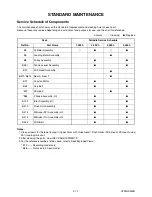
Page 57: ...l DECK ADJUSTMENTS 3 For the reference numbers listed above refer to Deck Exploded Views B73 Recording model only B86 Not used in 2 head model h Hours Cleaning I Replace Deck Periodic Service Schedule Ref No Part Name 1 000 h 2 000 h 3 000 h 4 000 h B2 Cylinder Assembly I I B3 Loading Motor Assembly I B8 Pulley Assembly I I B587 Tension Lever Assembly I I B31 ACE Head Assembly I B573 B574 Reel S R...

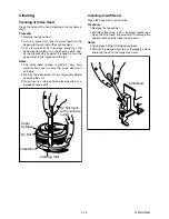
Page 58: ... hard material but since it is very thin avoid cleaning it vertically 2 Wait for the cleaned part to dry thoroughly before operating the unit 3 Do not reuse a stained head cleaning stick or a stained chamois cloth Cleaning of ACE Head Clean the head with a cotton swab Procedure 1 Remove the top cabinet 2 Dip the cotton swab in 90 isopropyl alcohol and clean the ACE Head Be careful not to damage th...

Page 59: ...2 Alignment Tape FL6N8 2 Head model FL6NS8 4 Head model Azimuth and X Value Adjustment of ACE Head Adjustment of Envelope Waveform J 2 Guide Roller Adj Screwdriver Available Locally Guide Roller J 3 Mirror Available Locally Tape Transportation Check J 4 Azimuth Adj Screwdriver Available Locally ACE Head Height J 5 Flat Screwdriver Available Locally X Value ...

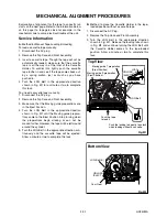
Page 60: ... that the Moving guide preparations are in the Eject Position 4 Turn the LDG Belt in the appropriate direction shown in Fig M1 until the Moving guide prepara tions come to the Eject Position Stop turning when the preparations begin clicking or can not be moved further However the tape will be left wound around the cylinder 5 Turn the LDG Belt in the appropriate direction con tinuously and the cass...

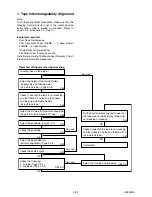
Page 61: ...asing and that there is no slack on the supply and take up side Guide Rollers Use a blank tape Adjust the height of the Guide Rollers Supply side and take up side Use a blank tape Page 2 3 3 Loading Use a blank tape Adjust the envelope Page 2 3 4 Check the envelope Adjust the Audio Section Azimuth Alignment Page 2 3 4 Check the audio output Check the following 1 X Value Page 2 3 3 2 Envelope Page ...

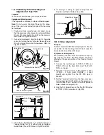
Page 62: ...6 1 B X Value Alignment Purpose To obtain maximum PB FM envelope signal at the pre set position of the Tracking Control Circuit align the Horizontal Position of the ACE Head Symptom of Misalignment If the Horizontal Position of the ACE Head is not prop erly aligned maximum PB FM envelope cannot be obtained at the preset position of the Tracking Control Circuit 1 Connect the oscilloscope to TP301 C...

Page 63: ... the enve lope becomes as flat as possible To do this adjust ment turn the top of the Guide Roller with the Guide Roller Adj Screwdriver 3 If the envelope is as shown in Fig M7 adjust the height of Guide Roller 2 Refer to Fig M3 so that the waveform looks like the one shown in Fig M9 4 If the envelope is as shown in Fig M8 adjust the height of Guide Roller 3 Refer to Fig M3 so that the waveform lo...

Page 64: ...heck the number of pushes to ensure preset position The number of pushes CH UP button to achieve 1 2 level of envelope should match the number of pushes CH DOWN button from center If required redo the X Value Alignment 1 E Checking and Alignment of Tape Path during reversing Purpose To make sure that the tape path is well stabilized dur ing reversing Symptom of Misalignment If the tape path is uns...

Page 65: ...ssembly T DM1H DM7H Desolder LDG Belt 2 S 3 9 9 ACE Head Assembly T DM1H DM7H S 4 10 2 Tape Guide Arm Assembly T DM1H DM8H 1 P 2 11 10 C Door Opener T DM1H DM8H 1 S 4A L 4 12 11 Pinch Arm B T DM1H DM8H 1 DM8H 2 P 3 13 12 Pinch Arm A Assembly T DM1H DM8H 1 DM8H 2 14 14 FE Head T DM1H DM9H S 5 15 15 Prism T DM1H DM9H S 6 16 2 Slider Shaft T DM10H L 5 17 16 C Drive Lever SP T DM10H 18 16 C Drive Leve...

Page 66: ...T Arm B DM2H DM14H P 5 34 26 Loading Arm SP Assembly B DM2H DM14H Refer to Alignment Sec Page 2 5 1 35 34 Loading Arm TU Assembly B DM2H DM14H Refer to Alignment Sec Page 2 5 1 36 16 26 M Brake TU Assembly HI T DM1H DM15H 37 2 26 M Brake SP Assembly HI T DM1H DM15H P 6 38 37 Tension Lever Assembly T DM1H DM15H 39 38 T Lever Holder T DM15H L 10 40 40 M Gear HI T DM1H DM15H C 6 41 15 40 Sensor Gear ...

Page 67: ...2 4 3 U29PHSDA 14 13 11 10 12 7 49 8 32 43 41 40 31 42 45 44 46 9 36 15 38 37 Fig DM1H Top View 34 19 35 25 26 24 23 27 33 20 28 22 Fig DM2H Bottom View ...

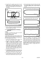
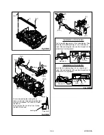
Page 68: ... Fig DM4H Pull up Slide 1 2 A 3 6 6 L 2 Pin A Hole A Pin B Hole B L 1 First insert 6 diagonally in 3 as shown below Then install 6 in 3 while pushing L 1 in a direction of arrow After installing 6 in 3 confirm that pin A of 3 enters hole A of 6 properly Installation of 3 and 6 View for A 2 1 4 Install 6 in 4 while pulling L 2 in a direction of arrow After installing 6 in 4 confirm that pin B of 4 ...

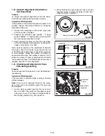
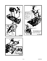
Page 69: ...th White Stripe A 8 Fig DM7H 11 13 12 10 L 4 P 3 P 2 Fig DM8H 1 Pin of 12 Pin of 10 Groove of 27 View for A When reassembling 10 and 12 confirm that pin of 10 and pin of 12 are in the groove of 27 as shown 27 Removal of 11 1 Remove screw S 4A 2 Unhook spring P 2 3 Release L 4 while holding 12 with a finger 4 Loosen a finger holding 12 and remove 11 A S 4A ...

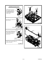
Page 70: ...r to Fig A Fig A 13 12 P 3 Fig B Top view Install pin of 12 in groove of 27 Refer to Fig B 27 Hold 12 and 13 till groove of pin of chassis looks and fit 13 in notch of chassis Then turn a few 13 while holding 12 Refer to Fig C Fig C Groove of pin of chassis Notch of chassis turn 13 12 Install 11 and 10 while holding 12 Refer to Fig DM8H 1 Fig DM8H 2 14 15 S 6 S 5 Fig DM9H 17 16 L 5 18 P 4 S 7 Fig ...

Page 71: ...2 4 7 U29PHSDA 19 Cap Belt S 8 19 20 Cap Belt A Installation position of Cap Belt View for A Fig DM11H L 6 22 20 C 1 21 27 Pin on 22 Position of pin on 22 turn Fig DM12H ...

Page 72: ...n 47 First groove on 27 Align 26 and 27 as shown Pin of 36 Pin of 33 Position of Mode Lever when installed Pin of 37 Bottom View Installation of 26 When reassembling 27 meet the first groove on 27 to the first tooth on 47 as shown Fig DM13H 2 32 L 9 P 5 34 35 Refer to the Alignment Section Page 2 5 1 33 Fig DM14H ...

Page 73: ...2 4 9 U29PHSDA 39 L 10 37 P 6 43 38 36 42 40 41 C 6 C 7 turn turn turn Fig DM15H 44 45 46 L 11 Fig DM16H Slide Plate S 11 47 48 Slide Fig DM17H ...

Page 74: ...mechanical or electrical parts Alignment points in Eject Position Alignment 1 Loading Arm SP and TU Assembly Install Loading Arm SP and TU Assembly so that their triangle marks point to each other as shown in Fig AL2 Alignment 2 Mode Gear Keeping the two triangles pointing at each other install the Loading Arm SP Assembly so that the last tooth of the gear meets the most inside teeth of the Mode G...

Page 75: ...lue grease SLIDUS OIL 150 Some Ref Numbers are not in sequence B12 B492 B11 B571 B37 B126 B8 B121 L1450 L1450 B86 L1466 B501 Chassis Assembly Top View Lubricating Point Chassis Assembly Bottom View Lubricating Point L1051 B35 B410 B411 B494 B567 L1053 B74 L1467 B553 B10 L1191 B73 B9 B2 TVCR 610 C L1322 B5 ...

Page 76: ...low grease B499 B516 B52 B507 B559 B581 B583 B580 B582 A View for A B578 B579 B579 B133 B551 Bottom Side Grease point Some Ref Numbers are not in sequence B488 B491 B513 Bottom Side Grease point L1151 B525 B31 L1406 B558 B557 B3 B592 B148 B522 B521 B590 B573 B574 B591 B416 B518 B564 B585 B487 B587 B508 B414 B572 B565 B568 B417 ...

Page 77: ...anism View 3 Mark Description Floil G 684G or Multemp MH D Blue grease SLIDUS OIL 150 L1341 L1321 B347 L1321 B355 B354 B482 B483 B425 B303 B555 B563 B300 B562 B514 B313 Some Ref Numbers are not in sequence B361 B359 B529 B360 ...

Page 78: ...I MK12 0VM101176 B492 MODE GEAR LM MK12 0VM204236 B494 C DOOR OPENER MK12 0VM305719 B499 T LEVER HOLDER MK12 0VM305729 B501 WORM HOLDER MK12 or 0VM203767 WORM HOLDER R MK12 0VM204324 B507 REEL WASHER MK9 5 2 1 0 5 0VM410058 B508 S BRAKE SPRING HI MK12 0VM414899 B513 P S W F 6 2 55 0 5 0VM402629A B514 SCREW RACK MK10 0VM411535 B516 REEL WASHER MK9 5 2 1 0 5 0VM410058 B518 P S W CUT 1 6X4 0X0 5T 0VM...

Page 79: ...TVCR 210 C TVCR 610 C HG2E0YD HG459YD 2004 08 06 ...

Reviews: