Rev 3
4
of 7
3.6.
Mounting
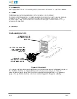
Alignment of needle-eyes is important when mounting connector to PC board. Entry clearance
between leading edge of needle-eyes and holes can be as low as .4 mm. Begin by gently lowering
connector to board, allowing leading edges of needle-eyes to guide themselves into the holes. Once
the object is lowered enough to contact thicker cross-section of needle, pressure should be added to
push pins through board to secure components together. For robotic assembly, alignment of
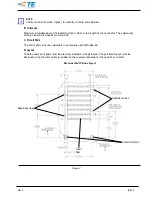
connector can be referenced from dimensions of board shown above in Figure 2.
3.7.
Soldering
A.
Process
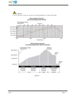
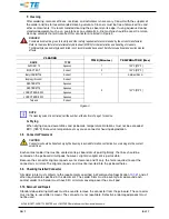
The connector must be soldered using non-focused infrared (IR) reflow or equivalent soldering
technique. Reflow temperature and time may vary depending on the size of the pc board and
placement of other components. This connector can be subjected to the reflow temperature and
approximate time specified in Figure 3.
B.
Solder Paste Characteristics
1. Alloy type for tin-lead solder shall be 63 Sn/37 Pb, 60 Sn/40 Pb, or 62 Sn/36 Pb/2 Ag.
2. Alloy type for lead-free solder shall be compatible with pure tin or gold, for example,
SAC305 (96.6 Sn/3 Ag/0.5 Cu) or SAC405 (95.5 Sn/4 Ag/0.5 Cu)
3. Flux incorporated in the paste shall be rosin, mildly active (RMA) type.
4. Paste will be at least 80% solids by volume.
5. Mesh designation shall be -200 to +325 (74 to 44 square micron openings, respectively).
6. Minimum viscosity of screen print shall be 5
10% cp (centipoise).
7. Minimum viscosity of stencil print shall be 7.5
10% cp (centipoise).
C.
Solder Volume
Minimum solder volume (V) (before curing) for each circuit pad is calculated as follows:
1.3 (pad length)x170%(open ratio)
0.31 (pad width)
0.15 (stencil thickness) = 0.103 mm³ (V).
NOTE
Solder volume may vary depending on solder paste composition.
D.
Solder Paste Thickness
Solder paste thickness for the connector contact solder tines must be at least 0.13.
E.
Stencil
The stencil aperture is determined by the circuit pad size and stencil thickness. It may be any shape,
provided it prevents solder bridging from one pad to another. The stencil should be 0.13 thick.
The stencil should include circuit pads for the contacts and holes for the stabilizers and hold-downs.
The stencil layout must be designed using the dimensions provided on the customer drawing for the
specific connector.
F.
Solder Mask
When soldering, solder mask is recommended between all circuit pads to minimize solder bridging
between pads. The mask must not exceed the height of the pad. If a trace is run between adjacent
pads on the pc board, a solder mask must be applied over the trace to prevent bridging and wicking
of solder away from the connector contact solder tines. Mask most suitable is Liquid Photo
Imageable.
It is recommended that component temperatures not exceed the temperatures and times given
in Figure 3.


