AN-000368
Document Number: AN-000368
Page 8 of 11
Revision: 1.0
5
THE SMARTMOTION SYSTEM DESIGN
This section is a system design overview and addresses MCU SAM G55 resource allocation.
5.1.
SYSTEM BLOCK DIAGRAM
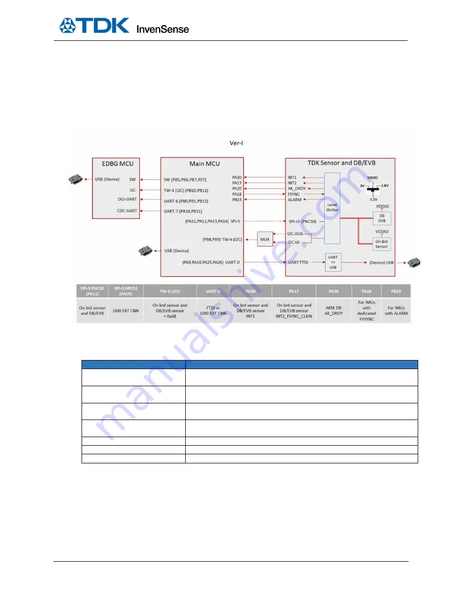
The on-board EDBG MCU AT32UC3A4256HHB-C1UR allows the user to do main MCU SAM G55 debug, trace, and
programming without using external tools. Figure 5 shows the system block diagram.
Figure 5. System Block Diagram
5.2.
MAIN MCU SAM G55 RESOURCE ALLOCATION
SAM G55 RESOURCE
USAGE
UART 0
(PA9/10/25/26)
The UART0 is connected to FTDI input by default. In the use case of Extension-1
on J200, the UART0 to FTDI connection can be disconnected through jumper J3.
TW6 (I
2
C)
(PB8/9)
TDK sensor is connected to this master I
2
C. On board sensor slave address =
0x69. Sensors on DB and EVB have slave address = 0x68.
SPI5
(PA05/PA11/12/13/14)
The SPI5 master is connected to TDK IMU sensor.
On board IMU /CS = PNCS1, EVB/DB IMU /CS = PNCS0.
GPIO (INTs)
PB03/PB15/PA30/PA20/PA15
The GPIOs are used for sensor interrupt inputs and other intelligent functions.
Refer to the table in Figure 5.
TW4 (I
2
C)
The master I
2
C communicates with EDBG MCU slave I
2
C.
UART6
The UART6 is used for EDBG DGI-UART interface.
UART7
The UART7 is used for EDBG CDC-UART interface.
Table 1. SAM G55 Resource Allocation


