background image

73M2901/5V 

Advanced Single 

Chip Modem 


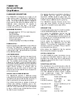
RESET 

A reset is accomplished by holding the RESET pin 
high.  To ensure a proper power-on reset, the reset 
pin must be held high for a minimum of 3

m

s.  At 

power on, the voltage at VPD, VPA, and RESET 
must come up at the same time for a proper reset.   

ASYNCHRONOUS AND SYNCHRONOUS SERIAL 
DATA INTERFACE 

The serial data interface consists of the TXD and 
RXD data paths (LSBit shifted in and out first, 
respectively); and the TXCLK and RXCLK serial 
clock outputs associated with the data pins; 

CTS

/

RTS

 flow control; 

DCR

DSR

 and 

DTR

.  In 

synchronous mode, the data is passed at the bit rate 
(tolerance is +1%, -2.5%). 


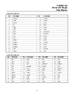
PIN DESCRIPTIONS 

POWER PIN DESCRIPTION 

PIN NAME 

32-PIN  44-PIN  TYPE  DESCRIPTION 

VPA 

15 

16 

Positive analog voltage (+ Analog Supply) 

VNA 

21 

22 

Negative analog voltage. (Analog Ground) 

VPD 

6, 25, 

29 

2,12, 

27, 33


Positive digital voltage (+ Digital Supply)  

VND 

5, 22, 

26 

11, 24, 

44, 28 

Negative digital voltage. (Digital Ground)  


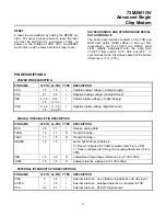
ANALOG INTERFACE PIN DESCRIPTION 

PIN NAME 

32-PIN  44-PIN  TYPE  DESCRIPTION 

RXA 

20 

21 

Receive analog data 

TXAN 

16 

17 

Transmit Analog - 

TXAP 

17 

18 

Transmit  

HBDEN 

14


15


I


2w/4w hybrid driver enable pin 

0 = Driver configured for  50k

W

 or greater load (Tie to VND)  

1 = Driver configured for driving line-coupling transformer (Tie to 
VPD) 


VBG


19 

20 

Analog Band Gap voltage reference pin (0.1

m

F to VNA) 

VREF 

18 

19 

Analog reference voltage pin (0.1

m

F to VNA) 


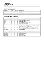
EXTERNAL INTERRUPTS PIN DESCRIPTIONS 

PIN NAME 

32-PIN  44-PIN  TYPE  DESCRIPTION 

RING 
ASRCH 
DTR 

32 

39 

38 

37 

External interrupt – Line interface ring detection circuitry input 

External interrupt – Autobaud detection, connected to TXD 

External interrupt – DTE DTR signal input 


Summary of Contents for 73M2901/5V

Page 1: ...ptions for a low power conventional 5 volt design with optional internal hybrid and country specific call progress support FEATURES Low overall system chip count True one chip solution for embedded sy...

Page 2: ...ybrid is to be used the on chip hybrid drivers can be reconfigured to drive a minimum load of 50kW and thus reduce the driver s power consumption The hybrid configuration is controlled by the state of...

Page 3: ...og voltage Analog Supply VNA 21 22 I Negative analog voltage Analog Ground VPD 6 25 29 2 12 27 33 I Positive digital voltage Digital Supply VND 5 22 26 11 24 44 28 I Negative digital voltage Digital G...

Page 4: ...O Serial output to DTE TXCLK 28 31 O Transmit Data Synchronous Clock TXD 27 30 I Serial data input from DTE USR10 12 8 I O This pin can optionally be configured as an active low detect pin This can b...

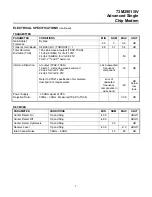
Page 5: ...ency 11 0592MHz 50ppm Operating Temperature 40C to 85 C TRANSMITTER PARAMETER CONDITIONS MIN NOM MAX UNIT ITU Guard Tone Power 550Hz relative to carrier 1800Hz relative to carrier 5 8 3 5 6 5 2 5 dB d...

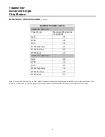
Page 6: ...high tone 6 0 DTMF low tone 8 0 DTMF total 3 9 Vref 1 25V VPA 5 0V QAM 9 6 DPSK 7 4 FSK 5 3 DTMF high tone 7 9 DTMF low tone 9 8 DTMF total 5 7 Note The recommended DAA see the TDK 73M2901 Reference M...

Page 7: ...3 dB Intermod Distortion At output TXAP TXAN 1 0kHz 1 2 kHz sine waves summed 2 0Vpk for Vref 1 25V 2 4Vpk for Vref 2 25V Refer to CTR21 specification for complete description of requirements sum of u...

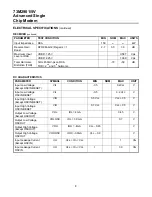
Page 8: ...ISTICS PARAMETER SYMBOL CONDITION MIN NOM MAX UNIT Input Low Voltage Except OSCIN RESET VIL 0 5 0 2Vcc V Input Low Voltage OSCIN RESET VIL 0 5 0 2 Vcc V Input High Voltage Except OSCIN RESET VIH 0 5 V...

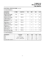
Page 9: ...m Digital Power Supply 5V IDDd 30pF pin 31 37 mA Maximum Analog Power supply 5V HBDEN pulled high IDDah1 30pF pin 20 25 mA Maximum Analog Power Supply 5V HBDEN pulled low IDDah0 30pF pin 4 6 mA Maximu...

Page 10: ...The firmware will automatically enter a power saving idle mode if the modem is on hook and there are no incoming host commands The modem automatically powers up upon receiving the next command This p...

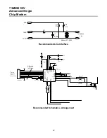
Page 11: ...dependent on the interface used between the pins and the line In order to save having to provide external op amps to drive the line coupling transformer the analog outputs TXAP and TXAN have the capa...

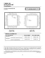
Page 12: ...1 2901_P32 1 2 3 4 5 6 7 8 9 10 11 12 13 14 15 16 17 18 19 20 21 22 23 24 25 26 27 28 29 30 31 32 ASRCH RING RELAY RI VND VPD DCD DSR CTS RTS USR11 USR10 LIU RST HBDEN VPA TXAN TXAP VREF VBG RXA VNA V...

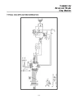
Page 13: ...73M2901 5V Advanced Single Chip Modem 13 TYPICAL USA APPLICATION SCHEMATICS...

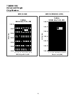
Page 14: ...002A Line 5 0V 25C 1 00E 00 1 00E 01 1 00E 02 1 00E 03 1 00E 04 4 10 11 12 13 14 15 16 17 18 19 8 12 16 20 24 28 32 36 40 44 1 00E 05 1 00E 06 1 00E 00 1 00E 01 1 00E 02 1 00E 03 1 00E 04 1 00E 05 1 0...

Page 15: ...LK 13 RESET 29 VPD 14 HBDEN 30 RXD 15 VPA 31 RXCLK 16 TXAN 32 DTR 44 PIN TQFP PIN OUT PIN PIN NAME PIN PIN NAME PIN PIN NAME PIN PIN NAME 1 N C 12 VPD 23 N C 34 N C 2 VPD 13 N C 24 VND 35 RXD 3 DCD 14...

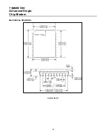
Page 16: ...73M2901 5V Advanced Single Chip Modem 16 MECHANICAL DRAWINGS 32 Pin PLCC...

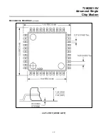
Page 17: ...73M2901 5V Advanced Single Chip Modem 17 MECHANICAL DRAWINGS continued 44 Pin TQFP JEDEC LQFP...

Page 18: ...infringements of patents and trademarks or other rights of third parties resulting from its use No license is granted under any patents patent rights or trademarks of TDK Semiconductor Corporation and...

Page 19: ...73M2901 5V Advanced Single Chip Modem 19 August 22 2001 Removed 5V pin callouts from package drawing August 30 2001 Updated Mechanical Drawing...

Reviews: