73M2901/5V
Advanced Single
Chip Modem
11
DESIGN CONSIDERATIONS
TDK Semiconductor’s single chip modem solutions
include all the basic modem functions. This makes
these devices adaptable to a variety of applications.
Unlike digital logic circuitry, modem designs must
contend with precise frequency tolerances and verify
low level analog signals, to ensure acceptable
performance. Using good analog circuit design
practices will generally result in a sound design.
The crystal oscillator should be held to a 50ppm
tolerance. Following are additional
recommendations that should be taken into
consideration when starting new designs.
LAYOUT CONSIDERATIONS
Good analog/digital design rules must be used to
control system noise in order to obtain high
performance in modem designs. The more digital
circuitry present in the application, the more
attention to noise control is needed.
High speed, digital devices should be locally
bypassed, and the telephone line interface and the
modem should be located next to each other near
where the telephone line connection is accessed. It
is recommended that power supplies and ground
traces should be routed separately to the analog and
digital portions on the board. Digital signals should
not be routed near low level analog or high
impedance analog traces.
The 73M2901/5V should be considered a high
performance analog device. A 10
m
F electrolytic
capacitor in parallel with a 0.1
m
F Ceramic capacitor
should be placed between VPD and VND as well as
between VPA and VNA. A 0.1
m
F ceramic capacitor
should be placed between VREF and VNA as well
as VBG and VNA. Use of ground planes and large
traces on power is recommended.
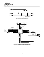
The 73M2901/5V is the first of a series of parts with
different and/or additional features. In order to insure
full lay out compatibility for all the series, it is
recommended to implement three additional
resistors in the schematics as shown in the
recommended schematics arrangement (R11, R12
and R13).
TELEPHONE LINE INTERFACE
Transmit levels at the line are dependent on the
interface used between the pins and the line. In
order to save having to provide external op-amps to
drive the line coupling transformer, the analog
outputs (TXAP and TXAN) have the capability to be
used as the hybrid drivers for connecting to the
transformer directly (with the required impedance
matching series resistor). Used in this configuration,
there is loss associated in both the receive path and
transmit path.
The line interface circuit shown on the following
page represents the basic components and values
3
for interfacing the TDK 73M2901/5V analog pins to
the telephone line.
MODEM PERFORMANCE
CHARACTERISTICS
The curves presented in this data sheet define
modem IC performance under a variety of line
conditions typical of those encountered over public
service telephone lines.
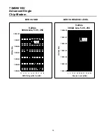
BER VS. SNR
This test represents the ability of the modem to
operate over noisy lines with a minimum amount of
data transfer errors. Since some noise is generated
in the best dial up lines, the modem must operate
with the lowest signal to noise ratio (SNR) possible.
Better modem performance is indicated by test
curves that are closest to the BER axis. A narrow
spread between curves representing the four line
parameters indicates minimal variation in
performance while operating over a range of
aberrant operating conditions. Typically a DPSK
modem will exhibit better BER performance test
curves receiving in the low band (answer mode)
than in the high band (originate mode).
BER VS. RECEIVE LEVEL
This test measures the dynamic range of the
modem. Because signal levels vary widely over dial
up lines, the widest possible dynamic range is
desirable. The SNR is held constant at the indicated
values as the Receive level is lowered from very a
very high to a very low signal level. The width of the
bowl of these curves, taken at the BER point is the
measure of the dynamic range.
3
TDK73M2901 Demo boards use the line interface shown on the
following page. Other designs may have different requirements
and thus will require different component values or a different
configuration. With the shown configuration, there is
approximately an 8dB loss in the transmit path, and approximately
a 5dB loss in the receive path.


