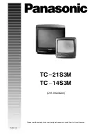
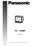
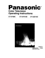
background image

A

A

B

B

C

C

D

D

E

E

4

4

3

3

2

2

1

1

TSOP 48 pin

VREF DECOUPLING

CLOSE TO 8202 PIN

0402 PUT ON NEARLY BGA

V2

Tan

TTE SHENZHEN R&D CENTER

<Doc>

YWX

2006-5-26

C

6

14

Wednesday, December 27, 2006

Title

Size

Document Number

Rev

Date:

Sheet

of

A_RA[0..11]
A_BA[0..1]

A_CLK

A_CKE

A_RAS#

A_CS#

A_WE#

A_CAS#

A_DQM[0..1]
A_DQ[0..31]

F_D[0..7]

F_OE#

A_DQS[0..3]

A_CLK#

VREF

F_D3

F_A14

F_A20

F_A17

IOA2
IOA3

F_A9

IOA7

F_A21

F_D4

F_A8

IOA0

IOA5

F_D6

F_D1

F_A13

IOA4

F_A10

IOA6

F_A18

IOA1

F_D2

F_D5

F_A16

F_A15

F_A19

PCE#

F_OE#

F_D0

F_D7

F_A[8..21]

FLASHVCC

D1V25

D1V25

D1V25

D1V25

D1V25

VREF

VREF

A_DQ19

A_CLK

A_DQ17

D_CLK

D_DQ14

D_RA6

D_DQ23

A_DQ8

D_DQ20

D_DQS1

D_DQM1

A_DQ25

D_DQ17

A_DQ1

D_RA8

D_DQ29

D_DQ24

D_DQS2

D_RA3

D_DQ3

D_DQM1

D_DQ8

D_RA7

D_CKE

D_DQ13

D_DQ1

A_RA2

D_RA9

A_DQM0

A_DQ4

D_DQ8

D_DQM0

A_DQ16

D_DQ6

D_RA5

A_DQ14

A_DQS1

D_DQ15

A_DQ26

D_CKE

D_CLK

A_DQS2

D_DQS3

D_DQ30

D_BA1

A_DQ13

A_CKE

D_RA6

A_DQ3

D_DQ6

A_RA3

D_RA2

D_RA3

D_DQS1

D_DQ15

D_DQ4

A_BA1

D_DQ5

A_DQ21

D_CLK#

D_CS#

D_DQ14

D_DQM1

D_DQ0

D_BA0

D_DQ22

A_DQS0

A_RA8

D_DQ22

A_DQ24

D_RA5

A_DQ0

D_DQ5

A_DQ29

A_DQ15

D_DQ11

A_DQ10

D_CS#

D_CLK#

D_DQS2

D_DQ24

D_DQ7

D_DQ13

D_RA1

D_DQ20

A_RA0

D_BA1

D_DQ23

A_RA9

A_BA0

A_DQ22

D_RA4

D_CAS#

A_DQM1

D_RA3

D_DQ4

A_CLK#

A_DQ27

D_CAS#

D_DQ19

D_DQS3

D_RAS#

A_DQ6

D_RA11

D_DQ25

VREF

D_DQ28

D_RA2

D_RA8

A_DQ12

D_BA0

D_DQ25

A_DQ9

D_DQ18

D_DQ12

D_DQ26

D_RA0

D_DQ26

VREF

A_RA11

D_RA4

D_WE#

D_DQ17

D_DQ12

D_RA11
D_RA9

A_DQ20

D_RA2

D_WE#

D_CLK

D_DQ31

D_DQ18

D_DQ11

A_RA1

D_RA10

A_DQ30

D_DQ2

D_DQ31

A_RA10

D_DQ16

D_RA10

D_DQ27

A_DQ5

D_RA1

D_BA0

D_DQ28

D_DQ27

A_DQ18

D_CKE

D_RA7

D_BA1

D_DQ2

A_DQ11

D_RA10

D_DQ10

D_DQM0

D_DQ29

D_DQ19

D_RAS#

D_RA9

A_DQ31

A_DQ2

D_DQ21

A_DQS3

D_RA8

D_DQ16

D_RA1

D_CLK#

D_DQ10

A_DQ23

D_DQM0

D_DQS0

D_RA0

D_DQ1

D_DQ9

D_DQS0

D_DQ0

D_DQ30

D_DQ21

A_DQ28

A_DQ7

D_DQ9

D_DQ3

D_RA11

D_RA0

D_DQ7

D_DQ6

D_DQ12

D_DQS3

D_DQM1

D_DQ11

D_DQS1

D_CAS#

D_DQ3

D_DQ24

D_DQ23

D_DQ28

D_DQS2

D_DQM0

D_DQ20

D_DQ30

D_DQ5

D_DQ16

D_WE#

D_DQ19

D_DQ22

D_DQ1

D_DQ13

D_DQS0

D_DQ18

D_DQ26

D_DQ14

D_DQ21

D_DQ15

D_DQ17

D_DQ31

D_DQ7

D_DQ4

D_DQ2

D_DQ8

D_DQ27

D_DQ29

D_DQ25

D_DQ10

D_DQ9

D_DQ0

D_RA9

DV25A

SDV25A

SDV25A

DV25B

A_RA4

A_RA7

A_RA6

D_RA4

D_RA7

D_RA6

D_RA5

A_RA5

A_RAS#

A_WE#

A_CAS#

A_CS#

D_CS#
D_RAS#

D_CAS#
D_WE#

D_RA2
D_RA1
D_RA0

D_RA3

D_RA6

D_RA7

D_RA5
D_RA4

D_RA10

D_BA1

D_BA0

D_RAS#

D_CS#

D_RA11

D_RA8

D_CLK

D_CLK

D_CLK

D_CLK#

D_CLK#

D_CLK#

F_A12

F_A11

IOA[0..7]

F_A[8..21]

PWR#

+5V

DV25A

SDV25

DV25A

DV25B

DV25A

DV25B

VREF

DV33B

A_RA[0..11]

[3]

A_BA[0..1]

[3]

A_CLK

[3]

A_CKE

[3]

A_RAS#

[3]

A_CS#

[3]

A_WE#

[3]

A_CAS#

[3]

A_DQM[0..1]

[3]

A_DQ[0..31]

[3]

F_D[0..7]

[3,6]

F_OE#

[3]

A_DQS[0..3]

[3]

A_CLK#

[3]

VREF

[3]

F_A[8..21]

[3,6]

DV25A

[3]

SDV25A

[3]

F_A[8..21]

[3,6]

IOA[0..7]

[3,6]

IOCE#

IOWR#

+5V

[1,2,4,6,8,9,10,11,12,13,14]

DV33B

[3]

SB33B

SB33B

SB33B

DV25B

SB33B

D1V25

VREF

DV25B

VREF

DV25B

D1V25

DV25A

DV25B

DV25B

DV25B

DV25B

DV25A

SDV25A

+5V

D1V25

DV33B

DV25B

C183
100PF

C0402/SMD

CB113

0.1uF

C0402/SMD

R65

75

CB82
0.1uF

CB70
0.1uF

CB79
0.1uF

R74

100K

RN21

47x4

1

2

3

4

5

6

7

8

RN10

47x4

1

2

3

4

5

6

7

8

R79

75

CB129

0.1uF

RN25

22x4

1

2

3

4

5

6

7

8

CB88
0.1uF

CB99
0.1uF

C46

3300pF

R62
0

R84

22

R81

75

CB90
0.1uF

CB77
0.1uF

RN19

47x4

1

2

3

4

5

6

7

8

CB72
0.1uF

C44

3300pF

R85

75

CB98
0.1uF

CB117

0.1uF

C0402/SMD

R64

22

CB102
0.1uF

CB78
0.1uF

CB106
0.1uF

CB64

0.1uF

U7

29LV160

25
24
23
22
21
20
19
18

8

9

28

47

16

29
31
33
35

7

26

38
40
42
44
30
32

10

36
39
41
43
45

37

27

11

15

34

46

6

4

5

3
2
1

48
17

13

12

14

A0
A1
A2
A3
A4
A5
A6
A7
A8

A19

OE

BYTE

A18

D0
D1
D2
D3

A9

CE

D4
D5
D6
D7
D8
D9

A20

D11
D12
D13
D14
D15

VCC

GND1

WE

RY/BY

D10

GND2

A10

A12

A11

A13
A14
A15
A16
A17

NC

RESET

WP/ACC

+

CE40

100uF/16v

CB126

0.1uF

RN8

47x4

1

2

3

4

5

6

7

8

+

CE42
100Uf/10v

R73

22

CB91
0.1uF

R78

22

C41

3300pF

R327

100/NC

CB67
0.1uF

C56
10uF/10v

C0805/SMD

CB125

0.1uF

RN13

47x4

1

2

3

4

5

6

7

8

CB116

0.1uF

C0402/SMD

C45

3300pF

L17

FB

R67

47

CB85
0.1uF

CB74
0.1uF

RN15

75x4

1

2

3

4

5

6

7

8

CB66
0.1uF

CB97
0.1uF

8M x 16

DDR

U5

M13S128168 8Mx16-5 

1
2
3
4
5
6
7
8
9

10
11
12
13
14
15
16
17
18
19
20
21
22
23
24
25
26
27
28
29
30
31
32
33

66
65
64
63
62
61
60
59
58
57
56
55
54
53
52
51
50
49
48
47
46
45
44
43
42
41
40
39
38
37
36
35
34

VDD
DQ0
VDDQ
DQ1
DQ2
VSSQ
DQ3
DQ4
VDDQ
DQ5
DQ6
VSSQ
DQ7
NC
VDDQ
LDQS
NC
VDD
DNU
LDM
WE
CAS
RAS
CS
NC
BA0
BA1
A10/AP
A0
A1
A2
A3
VDD

VSS

DQ15

VSSQ

DQ14
DQ13

VDDQ

DQ12
DQ11

VSSQ

DQ10

DQ9

VDDQ

DQ8

NC

VSSQ

UDQS

NC

VREF

VSS

UDM

CK
CK

CKE

NC

A12
A11

A9
A8
A7
A6
A5
A4

VSS

+

CE44

100Uf/10v

RN6

22x4

1

2

3

4

5

6

7

8

RN20

75x4

1

2

3

4

5

6

7

8

RN14

75x4

1

2

3

4

5

6

7

8

CB107
0.1uF

U6

SP2996B DDR Termination 8 PIN NSOIC

2

1

3
4

5

6

7

8

GND

VIN

REFEN
VOUT

VCNTL

VCNTL

VCNTL

VCNTL

R63
10k

R75

75

CB86
0.1uF

CB93

0.1uF

R328

100/NC

CB112

0.1uF

C0402/SMD

CB75
0.1uF

+

CE46

100Uf/10v

RN17

47x4

1

2

3

4

5

6

7

8

CB111

0.1uF

R83

75

CB71
0.1uF

R66

47

CB120

0.1uF

CB96
0.1uF

CB130
0.1uF

R71

22

CB87
0.1uF

CB65
0.1uF

CB122

0.1uF

CB114

0.1uF

C0402/SMD

+

CE45

33uF/16v

R76

22

R69

47

CB103
0.1uF

C40

3300pF

R61

10k

CB95
0.1uF

RN16

47x4

1

2

3

4

5

6

7

8

RN11

47x4

1

2

3

4

5

6

7

8

R329

100/NC

R72

75

CB118

0.1uF

C0402/SMD

CB108

0.1uF

CB110

0.1uF

+

CE47

33uF/16v

CB121

0.1uF

CB68
0.1uF

CB69
0.1uF

CB94
0.1uF

CB119

0.1uF

C0402/SMD

CB127

0.1uF

R169
100K

RN3

75x4

1

2

3

4

5

6

7

8

C42

3300pF

C55
3300pF

C0402/SMD

RN2

22x4

1

2

3

4

5

6

7

8

RN23

75x4

1

2

3

4

5

6

7

8

RN24

75x4

1

2

3

4

5

6

7

8

RN5

75x4

1

2

3

4

5

6

7

8

CB92
0.1uF

C43

3300pF

CB123

0.1uF

RN9

75x4

1

2

3

4

5

6

7

8

CB83
0.1uF

C172
10uF/10v

C0805/SMD

CB104
0.1uF

CB80
0.1uF

CB100
0.1uF

RN4

22x4

1

2

3

4

5

6

7

8

R82

22

RN22

75x4

1

2

3

4

5

6

7

8

CB76
0.1uF

CB124

0.1uF

C108
4.7uF/10v

C0805/SMD

R77

75

+

CE48

33uF/16v

R68

47

CB101
0.1uF

CB89
0.1uF

+

CE39

33uF/16v OS-CON/NC

C270UF16V/D10H12

CB73
0.1uF

CB128

0.1uF

C54
3300pF

C0402/SMD

U25

REGULATOR LT1084 TO-252-3

TO-252-3/SMD

3

1

2

IN

A

D

J

/G

N

D

OUT

R70

75

RN12

75x4

1

2

3

4

5

6

7

8

8M x 16

DDR

U4

M13S128168 8Mx16-5

1
2
3
4
5
6
7
8
9

10
11
12
13
14
15
16
17
18
19
20
21
22
23
24
25
26
27
28
29
30
31
32
33

66
65
64
63
62
61
60
59
58
57
56
55
54
53
52
51
50
49
48
47
46
45
44
43
42
41
40
39
38
37
36
35
34

VDD
DQ0
VDDQ
DQ1
DQ2
VSSQ
DQ3
DQ4
VDDQ
DQ5
DQ6
VSSQ
DQ7
NC
VDDQ
LDQS
NC
VDD
DNU
LDM
WE
CAS
RAS
CS
NC
BA0
BA1
A10/AP
A0
A1
A2
A3
VDD

VSS

DQ15

VSSQ

DQ14
DQ13

VDDQ

DQ12
DQ11

VSSQ

DQ10

DQ9

VDDQ

DQ8

NC

VSSQ

UDQS

NC

VREF

VSS

UDM

CK
CK

CKE

NC

A12
A11

A9
A8
A7
A6
A5
A4

VSS

L16

FB

+

CE41
47Uf/10v

CB84
0.1uF

CB109
0.1uF

C47

3300pF

RN18

75x4

1

2

3

4

5

6

7

8

R80

22

RN7

75x4

1

2

3

4

5

6

7

8

CB81
0.1uF

CB105
0.1uF

Summary of Contents for L42HDM61

Page 1: ...ment Procedure 9 4 Circuit Description 16 5 Schematic Diagram 30 6 PCB Layout 49 7 Explode View 51 8 BOM List 57 This manual is the latest at the time of printing and does not include the modification...

Page 2: ...er to the presence of uninsulated voltage within the products enclosure that may be of sufficient magnitude to constitute a risk of electric shock to the person The exclamation point within an equilat...

Page 3: ...nnel 8 Do not subject your television set to impact of any kind Be particularly careful not to damage the picture tube surface 9 Unplug this television set from the wall outlet before cleaning Do not...

Page 4: ...porting structure grounding of the lead in wire to an antenna discharge unit size of grounding conductors location of antenna discharge unit connection to grounding electrode and requirements for the...

Page 5: ...21 If you are unable to restorenormal operation by following the detailedprocedurein your operating instructions do not attempt any further adjustment Unplug the set and call your dealer or service te...

Page 6: ...iving 8 bits digital RGB pixels driving Color Temperature adjustable Cold Warm Standard adjustable Cold Warm Standard adjustable Cold Warm Standard Combfilter NTSC PAL Motion Adaptive 3D Comb Filter N...

Page 7: ...k Timer Functions 24h Time on off Sleep 24h Time on off Sleep 24h Time on off Sleep Local Controls Front menu volume up down Standby Power switch menu volume up down Standby Power switch menu volume u...

Page 8: ...Equipm Supplied Batteries of 1 5V 2 5 Batteries of 1 5V 2 5 Batteries of 1 5V 2 7 Dimension Unpacked stand included 1058 L x270 W x765 H 1062 L x305 W x770 H 1058 L x310 W x786 H Dimension Unpacked s...

Page 9: ...d y Supply 5v to JP12A and test the output of U30 U22 the normal is 3 3V 5 the U23 output should be 1 8V 5 y Download the SW to the main chip please see the chapter of how to download y Check all the...

Page 10: ...Red 3 High light white 4 Green 5 Blue 6 Continuous play 0 to 5 Other Back Light 254 Info Reset Power mode Remember Keep the lately Power on state OFF Standby after Power on Factory key Shortcut key O...

Page 11: ...Geo H Size 44 Nicam V POS 88 Mono V Size 68 Sound Other Info H V POS It is used for the position of the horizontal and Vertical H V Size It is used for the size of the horizontal and Vertical Factory...

Page 12: ...Default No need Adjusting Black Level 2 Default No need Adjusting Seamless OFF Default No need Adjusting It is only used for design please don t change Factory MT V System Project LCD32MT02Y1 Balance...

Page 13: ...n Other of the service menu Set OFF on Black expand in PICTURE of customer menu i White balance and color temperature adjusting on VGA state 1 On VGA state go into balance of service menu 2 Input 640h...

Page 14: ...nd white balance adjusting Flesh Tone and Adaptive Luma Control of Other in service menu should be set ON Black expand of Picture in customer menu should be set ON 3 4 Update the software The software...

Page 15: ...the key of the factory remote control After repeat that process 3 4 5 6 above please note when doing the process 6 must erase flash first press ERASE FLASH 3 5 The DDC data should be programmed before...

Page 16: ...deo input pins 2 Support 2 component input with SDTV format HDTV 480p 720p 1080i format 3 Support 1 VGA input up to SXGA 1280 1024 75hz including SOG singals 4 Support DVI 24 bit RGB signal input 1 2...

Page 17: ...S LIST Serial no Part no Name of IC function U3 13 MT8202 AGB LCDMT8202AG CPU video decoder scaler nicam decoder U4 U5 13 281622 ETB5 HY5DU281622ET 5 DDR SDRAM U7 13 AL016M 90B 16M S29AL016M90TFI02 FL...

Page 18: ...ng video input and output format up to HDTV It includes 3D comb filter TV decoder to retrieve the best image from popular composite signals Embedded HDTV VGA decoders let the high bandwidth input sign...

Page 19: ...us operations referenced to both rising and falling edges of the clock While all addresses and control inputs are latched on the rising edges of the CK falling edges of the CK Data Data strobes and Wr...

Page 20: ...5 3 U7 The S29AL016M is a 16Mbit 3 0 volt only flash memory organized as 2 097 152 bytes or 1 048 576 words 20...

Page 21: ...ion allows for the elimination of heat sinks in many applications The SC2602s are ideal for implementing DC DC converters needed to power advanced microprocessors in low cost systems or in distributed...

Page 22: ...e SP2996B provides an excellent voltage source for active termination schemes of high speed transmission lines such as those seen in high speed memory buses and distributed backplane designs when used...

Page 23: ...Typical Appliacations Circuit 5 6 U36 The CM2021 is a HDMI receiver port protection and interface device Electrical Schematic 23...

Page 24: ...MHz and video resolutions up to 1080p and UXGA The MT8293 supports the DVD Audio standard including 7 1 surround audio at 96kHz and stereo audio at 192kHz The built in High bandwidth Digital Content P...

Page 25: ...form at sample rates up to 200kHz per channel The CS5340 uses a 5th order multi bit Delta Sigma modulator followed by digital filtering and decimation which removes the need for an external anti alia...

Page 26: ...family is based on delta sigma modulation where the modulator output controls the reference voltage input to an ultra linear analog low pass filter This architecture allows for infinite adjustment of...

Page 27: ...m 1ch can be configured with one chip YDA138 has a Pure Pulse Direct Speaker Drive Circuit which directly drives speakers while reducing distortion of pulse output signal and reducing noise on the sig...

Page 28: ...ut RAMDAC or voltage output composite video source Low On Resistance and wide bandwidth make it dieal for video and other applications Also this device has exceptionally high current capability which...

Page 29: ...Block Diagram 29...

Page 30: ...umber Rev Date Sheet of GND GNDA URST GND AMP_GND AMP_ 12V 12V GNDP ON OFF GNDP URST 5V GNDP ON OFF SB 5V GNDA 8202UP3_0 12V 5V URST 1 3 6 9 GNDA 3 4 8 9 11 12 14 8202UP3_0 12V 1 2 9 10 11 12 14 5V 1...

Page 31: ...1117 adj SOT223 SMD 1 2 3 ADJ GND OUT IN CE17 100Uf 10v L7 FB L42 FB U24 AZ1117 adj NC SOT223 SMD 1 2 3 ADJ GND OUT IN CB197 0 1uF C0603 SMD FB FB2 R325 270 1 R38 100K L6 FB CE13 100Uf 10v CB18 0 1uF...

Page 32: ...RED 10 VGAVSYNC 10 CVBS2 12 SY0 12 ACENT SOY1 12 BLUE 10 AR 13 MPX2 12 VGASOG 10 PB1 12 CVBS1 12 PB0 12 Y0 12 SC0 12 Y1 12 AL 13 GREEN 10 GREEN 10 MPX1 12 PB0 12 PR0 12 SDA1 9 16 GPIO5 SCL1 9 16 IOA...

Page 33: ...DDB 3 DACVDDC 3 LVDDC 3 TESTP4 3 TESTN4 3 VFE_GND 2 3 10 11 LVDS_GND 2 3 14 AUDIO_GND 1 3 10 11 12 13 AADCVSS 1 3 10 11 12 13 VFE_GND1 2 3 11 12 REFP 3 REFN 3 GNDA 1 3 10 11 12 13 AADCVSS 1 3 8 9 10 1...

Page 34: ...ber Rev Date Sheet of SB18A SB33A SB18A 5VSB DV18A DV33A CB55 0 1uF C0402 SMD CB51 0 1uF C0402 SMD CE37 4 7uF 0805 C31 3300pF C0402 SMD CB59 0 1uF C0402 SMD CB56 0 1uF C30 3300pF C0402 SMD CB52 0 1uF...

Page 35: ...1uF C44 3300pF R85 75 CB98 0 1uF CB117 0 1uF C0402 SMD R64 22 CB102 0 1uF CB78 0 1uF CB106 0 1uF CB64 0 1uF U7 29LV160 25 24 23 22 21 20 19 18 8 9 28 47 16 29 31 33 35 7 26 38 40 42 44 30 32 10 36 39...

Page 36: ...D TMDS_D2 TMDS_D1 TMDS_GND TMDS_D1 TMDS_D0 TMDS_GND TMDS_D0 TMDS_CK TMDS_GND TMDS_CK CE_REMOTE_OUT DDC_CLK_OUT TP55 CB144 0 1uF CB152 0 1uF CB150 0 1uF C72 1000PF L27 FB CB143 0 1uF CB136 0 1uF C75 10...

Page 37: ...1 2 4 6 8 9 10 11 12 13 14 GPIO11 3 8 5V VGA_PLUGPWR VGA_PLUGPWR VGA_PLUGPWR 5V 5V 5V 5V SB33B R28 NC R132 68 R495 82 R350 47K D13 1N4148 QF6 2N7002 1 3 2 C89 10nF L56 FB C129 100nF R332 510 R139 82...

Page 38: ...DCVD ADCVA ADCVA 5V ADCVA ADCVL ADCVL DV33B 5V 5V DV33B DV33B DV33B 5V 5V 5V 5V 12V 12V 5V 5V ADCVL C104 1uF CB173 0 1uF CE60 4 7uF 25V R161 10K C179 0 01uF R167 10K NC CB167 0 1uF QF3 2N7002 1 3 2 FB...

Page 39: ...1 2 3 4 11 CCIR_VCLK 3 SDA0 3 10 SDA 1 6 8 11 SCL 1 6 8 11 CCIR_V 0 7 3 GPIO3 GPIO16 R 2 3 4 11 G 2 3 4 11 B 2 3 4 11 SCL0 3 10 SDA_V50 1 6 8 9 SCL_V50 1 6 8 9 SDA1 GPIO13 AVPB1N AVY1N AVPR1N AADCVSS...

Page 40: ...5 6 7 8 4 CE5 10U 16U R290 51 R280 5 1K R254 10K U38 CS4334 2 CH AUDIO DAC SOP8 SMD 1 2 3 4 5 6 7 8 SDATA DEM SCLK LRCK MCLK AOUTR AGND VA AOUTL C192 10uF 10v C0805 SMD R249 10K R267 5 1K L74 BCK 4235...

Page 41: ...ND1 2 3 4 8 9 10 DV33B 7 8 9 12 13 14 TU_CVBS0 12 14 TU_AURO 11 12 14 DV33B 7 8 9 12 13 14 5V 1 2 4 6 8 9 10 11 12 13 14 GPIO5 PWM1 TU_AULO 11 12 14 12V 1 2 9 10 11 12 14 C6 3 12 5V 12V TUNER 5V TUNER...

Page 42: ...5V ADC_IN2 3 11 PWM0 3 PWM1 3 IR 3 10 13 GPIO6 8202UP3_1 PWM_PANEL DV33B 7 8 9 12 13 14 5V 1 2 4 6 8 9 10 11 12 13 14 5V 5V 5V DV33B 5VSB 5V R33 NC R305 1k R306 10k L3 FB C178 0 01uF C0402 SMD C171 0...

Page 43: ...U_CVBS0 AU_IN_L AUSW0S1 TU_AULO 12V GNDV SCART1_FB GNDV ADC_IN1 GNDA AVY1N AVSC1 R 8202UP3_4 G B R AVCVBS2 AVCVBS3 AVSY0 AVPR1N AVPB1N AVY1N SC1 SY1 AVSC1 AVSY1 DV33B 5V A_MUTE A_MUTE 5V AU_IN_R AU_IN...

Page 44: ...1 6 3RCA_JACKAV JP604 2 1 NC 47pF C7 2 1 NC 47pF C21 5 4 3 2 1 PESD3V3L4UG D9 2 1 10K NC R43 2 1 18 R120 2 1 NC 47pF C14 2 1 100 FB17 1 2 3 4 CONN DIN4 JP607 2 4 3 5 1 6 3RCA_JACKAV JP605 2 1 10K NC R...

Page 45: ...22uF 35V CE21 2 1 47K R149 PCL_IN 1 PCR_IN 1 AUSW0S1 1 AV2R_IN 3 AV2L_IN 3 AV3R_IN 1 AV3L_IN 1 AV1R_IN 3 AV1L_IN 3 AUINR 1 AUINL 1 AUSW0S0 1 SWV120 SWV120 SWV120 SWV120 SWV120 SWV120 SWV120 SWV120 SW...

Page 46: ...23 22 21 20 19 16 15 14 13 12 18 6 17 4 11 7 8 10 5 2 3 9 1 JP601 CVBS_OUT CVBS_OUT CE13 10U 16V 0 1uF C204 10uF C205 100pF C207 100pF C208 10V100uF C206 GNDA SUB_WOOFER SWV120 SWV120 SUBWOOFER SUBWOO...

Page 47: ......

Page 48: ......

Page 49: ......

Page 50: ......

Page 51: ......

Page 52: ......

Page 53: ......

Page 54: ......

Page 55: ......

Page 56: ......

Page 57: ...56 3 7 3 3 3 79 3 3 5 3 7 3 3 2 2 5 9 7 00 00 00 25 7 3 7 3 3 2 2 5 9 7 00 00 00 25 3 7 3 3 2 2 5 9 7 00 00 00 25 6 3 7 3 3 2 2 5 9 7 00 00 00 25 3 7 3 3 2 2 5 9 7 00 00 00 25 3 7 3 3 2 2 5 9 7 00 00...

Page 58: ...1 3 7 0 6 5 1 75 1 0 6 5 3 7 0 6 5 1 75 1 0 6 5 3 7 0 6 5 1 79 25 6 7 27720 5 1 3 7 0 6 5 1 0 5 7 3 7 0 6 5 1 0 5 7 5 3 7 0 6 5 1 0 5 7 3 7 0 6 5 1 0 0 7 3 57 3 7 0 6 5 1 0 0 7 3 57 3 0 6 7 0 6 0 66 0...

Page 59: ...7 00 3 3 7 0 6 0 211 3 3 1 3 7 00 3 3 7 0 6 0 211 3 3 1 3 7 00 3 7 0 6 0 211 3 3 7 00 3 1 3 3 7 0 6 0 211 3 3 1 3 7 00 3 3 7 0 6 0 211 3 3 1 3 7 00 3 3 7 0 6 0 3 1 6 78 19 3 3 7 0 6 0 3 1 6 78 19 3 3...

Page 60: ...3 7 3 3 3 796 2 3 6 3 7 3 3 3 796 2 3 6 3 7 3 3 3 796 2 3 6 3 7 3 3 3 9 796 2 3 6 3 7 3 3 56 5 56 0 3 7 3 3 58 06 2 58 06 3 7 3 3 58 06 2 58 06 3 7 3 3 6 2 5 6 3 7 3 3 6 2 5 6 3 7 3 3 1 1 026 7 0 1 6...

Page 61: ...6 3 5 9 8 3 7 3 3 1 0 6 3 8 9 3 7 3 3 0 3 8 9 6 3 7 3 3 0 3 8 9 6 3 7 3 3 0 3 8 9 6 3 7 3 3 0 3 8 9 6 3 7 3 3 1 0 3 8 9 6 3 7 3 3 1 0 3 8 9 6 3 7 3 3 3 5 8 9 6 3 7 3 3 3 5 1 9 3 7 3 3 3 5 1 9 3 7 3 3...

Page 62: ...1 6 21 3 7 3 3 3 1 6 9 3 3 7 3 3 6 86 9 3 7 3 3 0 6 7 PP 25 4 3 7 3 3 0 6 7 PP 25 4 3 7 3 3 8 5 6 1 3 7 3 3 75 1 0 6 5 25 4 3 7 3 3 75 1 0 6 5 25 4 3 7 3 3 0 6 5 25 3 7 3 3 0 6 5 25 3 7 3 3 0 1 6 5 25...

Page 63: ...9 3 9 3 7 0 6 9 67 9 8 60 2 3 6 9 58 3 7 0 6 9 67 9 8 60 2 3 6 9 58 3 7 0 6 9 67 9 8 60 2 3 6 9 58 3 7 0 6 9 67 9 8 60 2 3 6 9 58 3 7 0 6 9 67 9 8 60 2 3 6 9 58 3 7 0 6 9 67 7 60 75 16 6725 00 7 7 131...

Page 64: ...6 9 67 7 60 5 6 2 0 5 3 7 0 6 9 67 7 60 5 6 2 0 5 3 7 0 6 9 67 7 60 5 6 2 0 5 3 7 0 6 9 67 7 60 5 6 2 0 5 3 7 0 6 9 67 7 60 5 6 2 0 5 3 7 0 6 9 67 7 60 5 6 2 0 5 3 7 0 6 9 67 7 60 5 6 2 0 5 3 7 0 6 9...

Page 65: ...7 7 60 2 8 3 7 0 6 9 67 1 17 3 2 0 3 7 0 6 9 67 1 17 3 2 0 3 7 0 6 9 67 1 17 3 2 0 3 7 0 6 9 67 1 17 3 2 0 3 7 0 6 9 67 1 17 3 2 0 3 7 0 6 9 67 1 17 3 2 0 3 7 0 6 9 67 1 17 3 2 0 3 7 0 6 9 67 1 17 3 2...

Page 66: ...1 4 3 7 0 6 0 67 7 60 75 16 6725 00 7 7 131 4 3 7 0 6 0 67 7 60 75 16 6725 00 7 7 131 4 3 7 0 6 0 67 7 60 75 16 6725 00 7 7 131 4 3 7 0 6 0 67 7 60 75 16 6725 00 7 7 131 4 3 7 0 6 0 67 7 60 75 16 6725...

Page 67: ...7 0 6 0 67 7 0 7 0 1 8 3 7 0 6 0 67 8 3 7 0 6 0 67 7 60 5 6 2 0 5 3 7 0 6 0 67 7 60 5 6 2 0 5 3 7 0 6 0 67 7 5 6 60 2 0 3 7 0 6 0 67 7 5 6 60 2 0 3 7 0 6 0 67 7 60 5 6 2 0 5 3 7 0 6 0 67 7 60 5 6 2 0...

Page 68: ...3 7 0 6 0 67 7 60 5 6 2 0 5 3 7 0 6 0 67 7 60 5 6 2 0 5 3 7 0 6 0 67 7 60 5 6 2 0 5 3 7 0 6 0 67 7 60 5 6 2 0 5 3 7 0 6 0 67 7 60 5 6 2 0 5 3 7 0 6 0 67 7 60 5 6 2 0 5 3 7 0 6 0 67 7 60 5 6 2 0 5 3 7...

Page 69: ...3 7 0 6 0 67 7 60 5 6 2 0 5 3 7 0 6 0 67 7 60 5 6 2 0 5 3 7 0 6 0 67 7 60 5 6 2 0 5 3 7 0 6 0 67 7 60 5 6 2 0 5 3 7 0 6 0 67 7 60 5 6 2 0 5 3 7 0 6 0 67 7 60 5 6 2 0 5 3 7 0 6 0 67 7 60 5 6 2 0 5 3 7...

Page 70: ...3 7 0 6 0 67 7 60 5 6 2 0 5 3 7 0 6 0 67 7 60 5 6 2 0 5 3 7 0 6 0 67 7 60 5 6 2 0 5 3 7 0 6 0 67 7 60 5 6 2 0 5 3 7 0 6 0 67 7 60 5 6 2 0 5 3 7 0 6 0 67 7 60 5 6 2 0 5 3 7 0 6 0 67 7 60 5 6 2 0 5 3 7...

Page 71: ...3 7 0 6 0 67 7 60 5 6 2 0 5 3 7 0 6 0 67 7 60 5 6 2 0 5 3 7 0 6 0 67 7 60 5 6 2 0 5 3 7 0 6 0 67 7 60 5 6 2 0 5 3 7 0 6 0 67 7 60 5 6 2 0 5 3 7 0 6 0 67 7 60 5 6 2 0 5 3 7 0 6 0 67 7 60 5 6 2 0 5 3 7...

Page 72: ...3 7 0 6 0 67 7 60 5 6 2 0 5 3 7 0 6 0 67 7 60 5 6 2 0 5 3 7 0 6 0 67 7 60 5 6 2 0 5 3 7 0 6 0 67 7 60 5 6 2 0 5 3 7 0 6 0 67 7 60 5 6 2 0 5 3 7 0 6 0 67 7 60 5 6 2 0 5 3 7 0 6 0 67 7 60 5 6 2 0 5 3 7...

Page 73: ...3 7 0 6 0 67 1 7 25 5 6 2 0 51 3 7 0 6 0 67 1 7 25 5 6 2 0 51 3 7 0 6 0 67 1 7 25 5 6 2 0 51 3 7 0 6 0 67 1 7 25 5 6 2 0 51 3 7 0 6 0 67 3 55 5 6 2 0 51 3 7 0 6 0 67 3 55 5 6 2 0 51 3 7 0 6 0 67 3 55...

Page 74: ...7 0 6 0 67 60 3 8 9 3 7 0 6 0 67 60 3 8 9 3 7 0 6 0 67 60 3 8 9 3 7 0 6 0 67 60 3 8 9 3 7 0 6 0 67 60 3 8 9 3 7 0 6 0 67 60 3 8 9 3 7 0 6 0 67 60 3 8 9 3 7 0 6 0 67 3 60 8 9 3 7 0 6 0 67 3 60 8 9 3 7...

Page 75: ...8 9 3 7 0 6 0 67 60 3 8 9 3 7 0 6 0 67 60 3 8 9 3 7 0 6 0 67 60 3 8 9 3 7 0 6 0 67 60 3 8 9 3 7 0 6 0 67 60 3 8 9 3 7 0 6 0 67 60 3 8 9 3 7 0 6 0 67 60 3 8 9 3 7 0 6 0 67 60 3 8 9 3 7 0 6 0 67 60 3 8...

Page 76: ...7 0 6 0 67 60 3 1 9 3 7 0 6 0 67 60 3 1 9 3 7 0 6 0 67 60 3 1 9 3 7 0 6 0 67 60 3 1 9 3 7 0 6 0 67 60 3 1 9 3 7 0 6 0 67 60 3 1 9 3 7 0 6 0 67 60 3 1 9 3 7 0 6 0 67 60 3 1 9 3 7 0 6 0 67 60 3 1 9 3 7...

Page 77: ...7 0 6 0 67 60 3 1 9 3 7 0 6 0 67 60 3 1 9 3 7 0 6 0 67 60 3 1 9 3 7 0 6 0 67 60 3 1 9 3 7 0 6 0 67 60 3 1 9 3 7 0 6 0 67 60 3 1 9 3 7 0 6 0 67 60 3 1 9 3 7 0 6 0 67 60 3 1 9 3 7 0 6 0 67 60 3 1 9 3 7...

Page 78: ...7 0 6 0 67 60 3 1 9 3 7 0 6 0 67 60 3 1 9 3 7 0 6 0 67 60 3 1 9 3 7 0 6 0 67 60 3 1 9 3 7 0 6 0 67 60 3 1 9 3 7 0 6 0 67 60 3 1 9 3 7 0 6 0 67 60 3 1 9 3 7 0 6 0 67 60 3 1 9 3 7 0 6 0 67 60 3 1 9 3 7...

Page 79: ...7 0 6 0 67 60 3 1 9 3 7 0 6 0 67 60 3 1 9 3 7 0 6 0 67 60 3 1 9 3 7 0 6 0 67 60 3 1 9 3 7 0 6 0 67 60 3 1 9 3 7 0 6 0 67 60 3 1 9 3 7 0 6 0 67 60 3 1 9 3 7 0 6 0 67 60 3 1 9 3 7 0 6 0 67 60 3 1 9 3 7...

Page 80: ...7 0 6 0 67 60 3 1 9 3 7 0 6 0 67 60 3 1 9 3 7 0 6 0 67 60 3 1 9 3 7 0 6 0 67 60 3 1 9 3 7 0 6 0 67 60 3 1 9 3 7 0 6 0 67 60 3 1 9 3 7 0 6 0 67 60 3 1 9 3 7 0 6 0 67 60 3 1 9 3 7 0 6 0 67 60 3 1 9 3 7...

Page 81: ...7 0 6 0 67 60 3 1 9 3 7 0 6 0 67 60 3 1 9 3 7 0 6 0 67 60 3 1 9 3 7 0 6 0 67 60 3 1 9 3 7 0 6 0 67 60 3 1 9 3 7 0 6 0 67 60 3 1 9 3 7 0 6 0 67 60 3 1 9 3 7 0 6 0 67 60 3 1 9 3 7 0 6 0 67 60 3 1 9 3 7...

Page 82: ...6 0 67 5 0 60 3 8 9 3 7 0 6 0 67 5 0 60 3 8 9 3 7 0 6 0 67 5 0 60 3 8 9 3 7 0 6 0 67 5 0 60 3 8 9 3 7 0 6 0 67 5 0 60 3 8 9 3 7 0 6 0 67 5 0 60 3 8 9 3 7 0 6 0 67 5 0 60 3 8 9 3 7 0 6 0 67 5 0 60 3 8...

Page 83: ...8 9 3 7 0 6 0 67 5 0 80 1 80 3 8 9 3 7 0 6 0 67 1 17 3 2 0 3 7 0 6 0 67 1 17 3 2 0 3 7 0 6 0 67 1 17 3 2 0 3 7 0 6 0 67 1 17 3 2 0 3 7 0 6 0 67 1 17 3 2 0 3 7 0 6 0 67 1 17 3 2 0 3 7 0 6 0 67 1 17 3 2...

Page 84: ...67 1 17 3 2 0 3 7 0 6 0 67 1 17 3 2 0 3 7 0 6 0 67 1 17 3 2 0 3 7 0 6 0 67 1 17 3 2 0 3 7 0 6 0 67 1 17 3 2 0 3 7 0 6 0 67 1 17 3 2 0 3 7 0 6 0 67 1 17 3 2 0 3 7 0 6 0 67 1 17 3 2 0 3 7 0 6 0 67 1 17...

Page 85: ...6 60 2 0 5 3 7 0 6 6 67 7 60 5 6 2 0 5 3 7 0 6 6 67 7 60 5 6 2 0 3 7 0 6 6 67 7 60 5 6 2 0 3 7 0 6 6 67 7 60 5 6 0 5 3 7 0 6 6 67 7 60 5 6 2 0 3 7 0 6 6 67 3 60 3 9 3 7 0 6 6 67 3 60 3 9 3 7 0 6 6 67...

Page 86: ...60 5 6 2 0 5 3 7 0 6 78 67 7 60 5 6 2 0 5 3 7 0 6 78 67 7 5 6 60 2 0 5 3 7 0 6 78 67 7 5 6 60 2 0 5 3 7 0 6 78 67 7 5 6 60 2 0 5 3 7 0 6 78 67 7 60 5 6 2 0 5 3 7 0 6 78 67 7 60 5 6 2 0 5 3 7 0 6 78 67...

Page 87: ...9 7 60 2 P 9 3 7 3 3 67 9 7 60 2 P 9 3 7 3 3 67 9 7 60 2 9 62 6 3 7 3 3 67 9 7 60 2 9 3 7 3 3 67 9 7 60 2 P 9 6 3 7 3 3 67 9 7 60 2 9 9 3 7 3 3 67 7 60 6 7 1 2 3 7 3 3 67 7 60 6 7 1 2 3 7 3 3 67 7 60...

Page 88: ...7 5 6 60 56 3 7 3 3 67 7 5 6 60 56 3 7 3 3 67 7 5 6 60 56 3 7 3 3 67 7 5 6 60 56 3 7 3 3 67 7 60 5 6 2 0 56 3 7 3 3 67 7 60 5 6 2 0 56 3 7 3 3 67 7 60 5 6 2 0 56 3 7 3 3 67 7 60 5 6 2 0 56 3 7 3 3 67...

Page 89: ...5 6 2 0 56 3 7 3 3 67 7 60 5 6 2 0 56 3 7 3 3 67 7 60 5 6 2 0 5 3 7 3 3 67 7 60 5 6 2 0 56 3 7 3 3 67 7 60 5 6 2 0 5 3 7 3 3 67 7 60 5 6 2 0 5 3 7 3 3 67 7 60 5 6 2 0 5 3 7 3 3 67 7 60 5 6 2 0 5 3 7 3...

Page 90: ...5 6 2 0 56 3 7 3 3 67 7 60 5 6 2 0 56 3 7 3 3 67 7 60 5 6 2 0 56 3 7 3 3 67 7 60 5 6 2 0 56 3 7 3 3 67 7 60 5 6 2 0 5 3 7 3 3 67 7 60 5 6 2 0 5 3 7 3 3 67 7 60 5 6 2 0 5 3 7 3 3 67 7 60 5 6 2 0 5 3 7...

Reviews: