31/01/96
Copyright TEL
2.5
Noise Mute (Squelch)
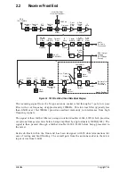
(Refer to Figure 2.2.)
The noise mute operates on the detected noise outside the audio bandwidth. An opera-
tional amplifier in IC304 is used as an active band pass filter centred on 70kHz to filter
out audio components. The noise spectrum is then further amplified in a variable gain,
two-stage amplifier (Q306 & Q307) with additional filtering. The noise is then rectified
(D301) and filtered to produce a DC voltage proportional to the noise amplitude. The
lowest average DC voltage corresponds to a high RF signal strength and the highest DC
voltage corresponds to no signal at the RF input.
The rectified noise voltage is compared with a threshold voltage set up on RV100, the
front panel mute potentiometer. Hysteresis is introduced by the feedback resistor
(R106) to prevent the received message from being chopped when the average noise
voltage is close to the threshold. R111 and R110 determine the mute opening and clos-
ing times. The mute control signal at pin 7 of IC100 is used to disable the speaker and
line audio outputs. The speaker output can be separately enabled for test purposes by
operating the front panel mute disable switch, SW100.
The mute control line is available on pad 101 (Rx gate out) for control of external cir-
cuitry. A high (9V) on pad 101 indicates that the audio is disabled and a low (0V) indi-
cates that a signal above the mute threshold level is being received.
The audio can also be disabled using the "Rx-disable" inputs, pads 100 or 113, having
connected the "Rx-disable" link between pins 1 & 2 of PL100. An adjustable time delay
(RV101) is provided on these lines. In order to disable the audio, either pad must be
pulled to 0V.
The red front panel LED (D102) indicates the status of the mute circuit. When a signal
above the mute threshold is received, the LED is illuminated. An undedicated relay is
provided (RL100) for transmitter keying or other functions and this can be operated
from the mute line by linking PL102.
2.6
Carrier Mute
(Refer to Figure 2.2.)
A high level carrier mute facility is also available. The RSSI (refer to Section 2.10) pro-
vides a DC voltage proportional to the signal strength. This voltage is compared with a
preset level, set up on RV104, and may be linked into the mute timing circuit using
PL104. PL104 selects either the noise mute or the carrier mute. From this point both
mute circuits operate in the same manner, using common circuitry.
Summary of Contents for T830 Series
Page 10: ...31 01 96 Copyright TEL...
Page 12: ...31 01 96 Copyright TEL...
Page 16: ...31 01 96 Copyright TEL...
Page 20: ...31 01 96 Copyright TEL...
Page 22: ...31 01 96 Copyright TEL...
Page 24: ...31 01 96 Copyright TEL...
Page 28: ...31 01 96 Copyright TEL...
Page 30: ...31 01 96 Copyright TEL...
Page 32: ...31 01 96 Copyright TEL...
Page 38: ...31 01 96 Copyright TEL...
Page 40: ...31 01 96 Copyright TEL...
Page 62: ...31 01 96 Copyright TEL...
Page 68: ...31 01 96 Copyright TEL...
Page 70: ...31 01 96 Copyright TEL...
Page 84: ...31 01 96 Copyright TEL...
Page 88: ...31 01 96 Copyright TEL...
Page 94: ...31 01 96 Copyright TEL...
Page 98: ...31 01 96 Copyright TEL...
Page 108: ...31 01 96 Copyright TEL...
Page 110: ...31 01 96 Copyright TEL...
Page 116: ...31 01 96 Copyright TEL...
Page 118: ...31 01 96 Copyright TEL...
Page 140: ...31 01 96 Copyright TEL...
Page 142: ...31 01 96 Copyright TEL...
Page 148: ...31 01 96 Copyright TEL...
Page 160: ...31 01 96 Copyright TEL...
Page 162: ...31 01 96 Copyright TEL...
Page 166: ...31 01 96 Copyright TEL...
Page 172: ...31 01 96 Copyright TEL...
Page 180: ...31 01 96 Copyright TEL...
Page 190: ...31 01 96 Copyright TEL...
Page 192: ...31 01 96 Copyright TEL...
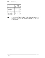
Page 196: ...31 01 96 Copyright TEL 1 3 Versions Description Version 10 136 174MHz...
Page 198: ...31 01 96 Copyright TEL...
Page 204: ...31 01 96 Copyright TEL...
Page 212: ...31 01 96 Copyright TEL...
Page 218: ...31 01 96 Copyright TEL...
Page 220: ...31 01 96 Copyright TEL...
Page 222: ...31 01 96 Copyright TEL...
Page 224: ...31 01 96 Copyright TEL...
Page 228: ...31 01 96 Copyright TEL...
Page 232: ...31 01 96 Copyright TEL...
Page 236: ...31 01 96 Copyright TEL...
Page 238: ...31 01 96 Copyright TEL...
Page 240: ...31 01 96 Copyright TEL...
Page 243: ...T800 Memory PCB IPN 220 01144 00 Top Side Copyright TEL 31 01 96...
Page 244: ...31 01 96 Copyright TEL T800 Memory PCB IPN 220 01144 00 Bottom Side...
Page 246: ...E2 6 T800 Memory PCB Information M830 00 31 01 96 Copyright TEL...
Page 250: ...31 01 96 Copyright TEL...
Page 251: ...T830 VCO PCB IPN 220 01176 01 Bottom Side Copyright TEL 31 01 96...
Page 252: ...31 01 96 Copyright TEL T830 VCO PCB IPN 220 01176 01 Top Side...
Page 253: ...M830 00 T830 VCO PCB Information E3 7 Copyright TEL 31 01 96 T830 VCO 220 01176 01...
Page 254: ...E3 8 T830 VCO PCB Information M830 00 31 01 96 Copyright TEL...
Page 256: ...31 01 96 Copyright TEL...
Page 260: ...31 01 96 Copyright TEL...
Page 264: ...31 01 96 Copyright TEL...
Page 272: ...31 01 96 Copyright TEL...
Page 278: ...31 01 96 Copyright TEL...
Page 284: ...31 01 96 Copyright TEL...


