13
Chapter 1: Introduction
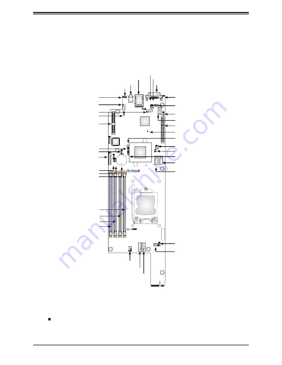
Figure 1-5. Motherboard Layout
1.5 Motherboard Layout
Below is a layout of the X11SSD-F with jumper, connector and LED locations shown. See
the table on the following page for descriptions. For detailed descriptions, pinout information
and jumper settings, refer to Chapter 4.
Notes:
•
" " indicates the location of pin 1.
•
Jumpers/LED indicators not indicated are used for testing only.
X11SSD-F
REV:1.00
DESIGNED IN USA
BAR C
ODE
J4
BT1
SW1
S-SGPIO1
LED2
A
C
LED1
A
C
JSTBY1
JBT1
FAN1
JTPM1
JBR1
JI2C2
JI2C1
J5
JPME2
JPB1
JPG1
JWD1
JVRM2
JVR1
JVRM1
LED3
A
C
DIMMA1
DIMMA2
DIMMB1
DIMMB2
SAS1
SAS0
I-SATA2 I-SATA3
JIPMB1
JSMB1
CPU1 MICRO-LP
PCI-E 3.0 X8
CPU1 SLOT1 PCI-E 3.0 X8
KVM
USB2(3.0)
CPU Socket
LGA1151
IPMI_LAN
UID
JSD1
SATA DOM POWER
SATA DOM+POWER
Intel
C236
S-SGPIO1
J4
JPG1
DIMMA1
DIMMB2
DIMMA2
DIMMB1
JWD1
JSTBY1
JBT1
BT1
J5
I-SATA3
JSD1
JTPM1
UID
JIPMB1
MICRO LP
JI2C1
JI2C2
I-SATA2
USB2 (3.0)
FAN1
LED1
IPMI_LAN
KVM
SLOT1
JBR1
JPME2
LED2
SW1
LED3
JPB1
SAS0
SAS1
JSMB1
JVRM1
JVRM2


