UM1996
Getting
started
DocID028716 Rev 2
11/29
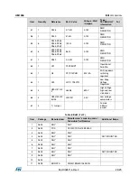
Pin Default
Signal
Solder
Bridge
8
9
GND
10
NC
11
GPIO/DAC/PWM
R80 N.M.
12
PA12
CPOUT
R52
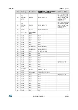
13
BKIN
R78
14
PA11
BKIN
R73
15
UL - TIM1_CH1N
R58
16
PB12
17
PB6
18
PB11/NC
For NUCLEO-F401RE: remove the R60
resistor if 6-Step control is used (X-CUBE-SPN8)
BEMF2
R60
19
PC7
20
GND
21
PA9
VH - TIM1_CH2
R64
22
PB2
LED RED
R83
23
PA8
UH - TIM1_CH1
R56
24
PB1
WL
–
TIM1_CH3N
R72
25
PB10
Encoder Z/ Hall H3
R84
26
PB15
UL
–
TIM1_CH1N
R86
27
PB4
CURRENT REF
R77
28
PB14
BKIN
R74
29
PB5
GPIO/DAC/PWM
R85
30
PB13
GPIO/DAC/PWM
R82 N.M.
31
PB3
Encoder B/ Hall H2
R81
32
AGND
33
PA10
WH - TIM1_CH3
R70
34
PC4
BEMF2
R61
35
PA2
36
NC/PF5
37
PA3
38
NC/PF4
Notes:
(1)
U5V is 5 V power from ST-LINK/V2-1 USB connector and it rises 5 V
(2)
For NUCLEO-F302R8 - pin PA5 is on CN10/pin 30 and PB13 is on CN10/pin 11
(3)
For NUCLEO-F302R8 - pin PA6 is on CN10/pin 28 and PB14 is on CN10/pin 13
(4)
For NUCLEO-F302R8 - pin PA7 is on CN10/pin 26 and PB15 is on CN10/pin 13


