

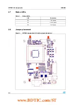


STPM01 programmer kit schematics
UM0509
12/21
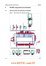
4
STPM01 programmer kit schematics
4.1
Microcontroller and main parts schematic
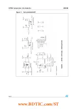
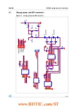
Figure 7.
Microcontroller and main parts schematic
not
Re
s
e
t
BOOTEN
+3V3
GND
TX_1_I
/0
0
_x
T
0
_x
T
JTMS
DBGRQS
not
Re
s
e
t
JTCK
not
JTRST
JTDO
JTDI
+3V3
GND
A1
A3
A4
A5
A6
A7
A8
A9
A10
A11
A12
A13
A16
A17
A18
CS.
1
A15
A14
D0
D12
D8
D9
D14
D5
D4
D7
D11
D3
D1
D10
D2
D15
D6
D13
+3V3
GND
A2
nW
E0
nW
E1
nRD
A19
VOUT
+1V8
VBKP
+5V
+3V3
GND
GND
+3V3
+5V
+1V8
W
AKEUP
GND
JTDI
JTDO
not
JTRST
JTMS
JTCK
MOSI
SCLK
MI
SO
GND
not
Re
s
e
t
DBGRQS
Rx
_0
+5V
+3V3
GND
+5V
P1.
0
P1.
1
P1.
2
P0.
1
0
P0.
7
+5V
+3V3
P0.
0
P0.
6
P0.
2
P0.
4
P0.
5
+3V3
GND
+3V3
GND
CK
I
T
X
C
T
RI
T
X
C
T
R
O
T
X
C
T
RO
T
X
C
T
R
SY
STEM_DEFAULT
WAKEUP
+3V3
VBKP
GND
not
Re
s
e
t
GND
Tx
_0
GND
RTCXTI
JTMS
126
P0.
2
P0.
4
P0.
0
RTCXTO
P0.
1
SY
STEM_DEFAULT
CK
P0.
7
P0.
6
JTDI
JTCK
BOOTEN
not
JTRST
JTDO
P0.
1
0
P0.
5
Rx
_0
DBGRQS
CS.
1
nRD
rn
1
2
A23
A22
A0
A1
A2
A3
A4
A5
A6
A7
A8
A9
A10
A11
A12
A13
A14
A15
A16
A17
A18
A19
A20
A21
D15
D14
D13
D12
D11
D10
D9
D8
D7
D6
D5
D4
D3
D2
D1
D0
Cn
P1.
6
+1V8
VBKP
rn
1
3
nW
E0
nW
E1
rn
1
4
ORANGE
TX_1_I
/0
P1.
0
P1.
1
P1.
2
7
11
12
18
23
24
25
26
27
28
29
75
76
85
19
20
37
39
41
43
48
10
4
111
108
107
89
88
74
45
90
91
106
105
110
109
87
70
69
68
60
57
56
53
66
VBKP
+5V
+1V8
+3V3
+3V3
+3V3
+3V3
POWER
ESD
POW
E
R M
ANAGEM
E
NT
GN
D
+3V
3
+5V
+1V
8
VBKP
R4
560
R4
560
U2
ESDA6V1-
5W
6-
SOT323-
6L
U2
ESDA6V1-
5W
6-
SOT323-
6L
I/O
1
1
I/O
2
3
I/O
3
4
I/O
4
5
I/O
5
6
GN
D
2
CHARGE PUM
P
Cha
rge
Pump
+5V
0
STR7
_
O
T
P
_
E
N
STR7
_
SBS
STR7
_
SBG
GN
D
STPM
0
1
_
SDA
S
T
P
M
01_S
C
S
S
T
P
M
01_S
Y
N
STPM
0
1
_
SCL
J9
Enable
UART0 TX
J9
Enable
UART0 TX
1
2
EM
I_SRAM
not
C
S
_S
R
A
M
not
O
E
WE
1
WE
0
D0
D1
D2
D3
D4
D5
D6
D7
D1
3
D1
5
D1
2
D8
D1
4
D1
0
D9
D1
1
GN
D
+3V
3
A1
A2
A3
A4
A5
A6
A7
A8
A9
A1
1
A1
0
A1
2
A1
3
A1
4
A1
5
A1
6
A1
7
A1
8
A1
9
VO
UT
R1
560
R1
560
R5
22
R5
22
R7
22
R7
22
SW
1
MOMENTARY
SW
1
MOMENTARY
R9
22
R9
22
BOOT
BOOT
B
OOT
_
E
N
SW
2
SW
1
+3V
3
GN
D
U3
ESDA6V1-
5W
6-
SOT323-
6L
U3
ESDA6V1-
5W
6-
SOT323-
6L
I/O
1
1
I/O
2
3
I/O
3
4
I/O
4
5
I/O
5
6
GN
D
2
R3
560
R3
560
GENERAL
USB
SYSTEM
RTC
STS
ADC
CAN
I2C0
SPI0
SPI1
UART0
UART1
UART2
DEBUG
TIMER1
GPIO PORT
EMI
SUPPLY
U1
STR710FZ2T6-
TQFP144
GENERAL
USB
SYSTEM
RTC
STS
ADC
CAN
I2C0
SPI0
SPI1
UART0
UART1
UART2
DEBUG
TIMER1
GPIO PORT
EMI
SUPPLY
U1
STR710FZ2T6-
TQFP144
P
2
.0
/C
S
.0
7
P2
.1
/C
S.
1
8
P2
.2
/C
S.
2
11
P2
.3
/C
S.
3
12
A.
0
98
A.
1
99
A.
2
100
A.
3
101
A.
4
102
A.
5
114
A.
6
115
A.
7
116
A.
8
117
A.
9
118
A.
1
0
119
A.
1
1
120
A.
1
2
121
A.
1
3
122
A.
1
4
130
A.
1
5
131
A.
1
6
132
A.
1
7
133
A.
1
8
134
A.
1
9
135
P
2
.4
/A
.2
0
13
P
2
.5
/A
.2
1
14
P
2
.6
/A
.2
2
15
P
2
.7
/A
.2
3
17
D.
0
61
D.
1
62
D.
2
63
D.
3
64
D.
4
65
D.
5
78
D.
6
79
D.
7
80
D.
8
81
D.
9
82
D.
1
0
92
D.
1
1
93
D.
1
2
94
D.
1
3
95
D.
1
4
96
D.
1
5
97
RD
2
WE
.0
137
WE
.1
136
P2
.8
18
P2
.9
23
P2
.1
0
24
P2
.1
1
25
P2
.1
2
26
P2
.1
3
27
P2
.1
4
28
P2
.1
5
29
P
1
.4
/T
1
.IC
A
P
A
75
P
1
.5
/T
1
.IC
A
P
B
76
P1
.6
/T
1
.O
C
M
P
B
77
P1
.7
/T
1
.O
C
M
P
A
85
VSS1
42
VSS2
59
VSS3
84
VSS4
103
VSS5
112
VSS6
128
VSS7
139
VSS8
5
VSS9
21
P0.1
5/W
AKEUP
47
STBY
51
V33.
1
6
V33.
2
22
V33
.3
40
V33
.4
83
V33
.5
104
V33
.6
113
AVDD
66
V18
.1
58
V18
.2
129
V18B
KP
55
CK
46
P1
.8
86
P1
.9
105
P1
.1
0
/USBCL
K
106
USBDN
91
USBDP
90
RST
IN
52
CKO
U
T
45
RT
CXT
I
49
RT
CXT
O
50
BO
O
T
EN
16
JT
D
I
30
JT
M
S
31
JT
C
K
32
JT
D
O
33
JT
R
S
T
34
P1
.0
/T
3
.O
C
M
PB/
AI
N.
0
71
P
1
.1
/T
3
.IC
A
P
A
/A
IN
.1
72
P1
.2
/T
3
.O
C
M
PA/
AI
N.
2
73
P
1
.3
/T
3
.IC
A
P
B
/A
IN
.3
74
P1
.1
1
/CANRX
88
P
1.
12/
C
A
N
T
X
89
P
1.
13/
H
C
LK
/I
O
.S
C
L
107
P
1.
14/
H
C
LK
/I
O
.S
C
L
108
P1
.1
4
/HTXD
111
P0
.0
/S0
.M
ISO
/U
3
.T
X
123
P0
.1
/S0
.M
O
SI
/U
3
.RX
124
P
0.
2
/S
0.
S
C
LK
/I
1.
S
C
L
125
P0
.3
/S
0
.SSN/
I1
.S
DA
126
P0
.4
/S
1
.M
ISO
127
P0
.5
/S
1
.M
O
SI
140
P
0.
6
/S
1.
S
C
LK
141
P0
.7
/S1
.SSN
142
P
0
.8
/U
0
.R
X
/U
0
.T
X
143
P
0
.9
/U
0
.T
X
/B
O
O
T
.0
144
P
0
.1
0
/U
1
.R
X
/U
1
.T
X
1
P0
.1
1
/U1
.T
X/
BO
O
T
.1
3
P0
.1
2
/SCCL
K
4
P
0
.1
3
/U
2
.R
X
/T
2
.O
C
M
P
A
9
P0
.1
4
/U4
.T
X/
T2
.I
CAPA
10
D
B
GR
OS
44
NC
35
TEST1
36
TEST2
38
VSSBKP
54
AVSS
67
NC
19
NC
20
NC
37
NC
39
NC
41
NC
43
NC
48
NC
53
NC
56
NC
57
NC
68
NC
69
NC
70
NC
87
NC
109
NC
110
NC
60
V33.
7
138
R8
22
R8
22
RESET
RESET
GN
D
+3V
3
CLK - RTC
CLK
CK
RT
CXT
I
RT
CXT
O
+3V
3
GN
D
TP10TP10
1
C49
10uF
C49
10uF
SW
2
MOMENTARY
SW
2
MOMENTARY
C1
100n
C1
100n
C2
100n
C2
100n
R2
560
R2
560
OPTO ISOLATED UART
UARTx
GN
D
+3V
3
+5V
TX_0
RX_
0
JTAG
JT
M
S
not
JTR
s
t
JT
D
I
JT
C
K
JT
D
O
D
B
GR
QS
not
R
e
se
t
+3V
3
GN
D
R6
560
R6
560
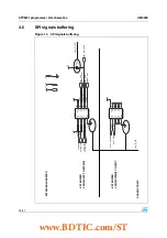
SPI_BUFFER
SPI
_BUFFER
GN
D
STR7
_
R
EAD_
EN
ST
R7
_
S
CS
STR7
_
W
RI
T
E
_
E
N
STR7
_
M
O
S
I
STR7
_
M
ISO
ST
R7
_
S
CL
STR7
_
SYN
STPM
0
1
_
SCS
S
T
P
M
01_S
D
A
S
T
P
M
01_S
C
LK
STPM
0
1
_
S
YN
5V
3.
3V
www.BDTIC.com/ST


