


16
Hardware Setup
Cache Configuration
The mainboard has a write-back caching scheme. You can configure the
mainboardÕs cache by installing cache chips in the sockets noted below
and then set jumpers JP31 to set the mainboard for the type of SRAM
installed. See Figures 2Ð3Ð1~2Ð3Ð2 for cache configurations.
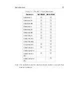
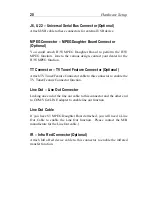
Cache Size and RAM Locations
Cache Size
Cache RAM
TAG RAM
Cacheable
Range
256KB
32K x32, 2 pcs
(or 256K module)
on U31, U32 (or J3)
16K x 8
on U27, U28
512 MB
Upgrade to
512KB
32K x 32, 2pcs +
256K module
on U31, U32, and J3
16K x 8
on U27, U28
512 MB
Onboard
512KB
64K x 32, 2pcs
on U31, U32
16K x 8
on U27, U28
512 KB
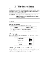
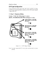
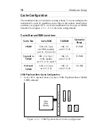
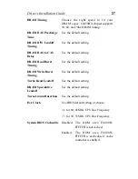
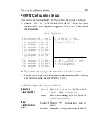
256K Pipelined Burst Cache Configuration
1. Leave JP31 opened when you have 256K Pipelined Burst SRAM
CHIPs onboard.
586
CPU
Family
TAG
TAG
P.B. SRAM
32k x 32
P.B. SRAM
32k x 32
Pipelined Burst SRAM Module Slot
JP31
Figure 2Ð3Ð1. 256K Pipelined Burst Cache Configuration