background image

Section 4

Replacement of Main Parts

CAUTION

Be sure to set the all POWER switches to OFF and unplug the all power cords before starting any of the
replacement work.
If the replacement work is attempted with the power ON, it may result in electric shock or damage of circuits.

4-1. 

Tightening Torque

When tightening screws used in this unit, be sure to use a torque driver and tighten screws to the specified tightening
torque.

Tightening torque
PSW 3x6 : 0.80 ±0.12 N·m
PSW 3x30 : 0.80 ±0.12 N·m
M3 (Shoulder screw) : 0.80 ±0.12 N·m

Tip

When using the torque driver with the notation of cN·m, interpret it as follows.
Example:0.8 N·m = 80 cN·m

XVS-8000-C/XVS-8000

4-1

Summary of Contents for XKS-8160

Page 1: ...D XKS 8160 MIX EFFECT BOARD XKS 8210 FRAME MEMORY BOARD XKS 8440 FORMAT CONVERTER BOARD XKS 8460 HD DME BOARD XKS 8470 SDI INPUT CONNECTOR BOARD XKS S8110 SDI OUTPUT CONNECTOR BOARD XKS S8165 IP INPUT CONNECTOR BOARD XKS T8110 IP OUTPUT CONNECTOR BOARD XKS T8165 SERVICE MANUAL 1st Edition ...

Page 2: ...aben in der Anleitung zu befolgen Andere als die angegeben Wartungsarbeiten dürfen nur von Personen ausgeführt werden die eine spezielle Befähigung dazu besitzen AVERTISSEMENT Ce manual est destiné uniquement aux personnes compétentes en charge de l entretien Afin de réduire les risques de décharge électrique d incendie ou de blessure n effectuer que les réparations indiquées dans le mode d emploi...

Page 3: ... これらは 現在サポートされていません For safety do not connect the connector for periph eral device wiring that might have excessive volt age to the following ports MVS LAN connectors UTL LAN connectors Follow the instructions for the above ports When using the following connector use a shiel ded type cable to prevent malfunction due to radiation noise XVS 8000 MVS LAN and UTL LAN connectors XKS T8810 XKS T8165 LA...

Page 4: ...n 注意 指定以外の電池に交換すると 破裂する危険があり ます 必ず指定の電池に交換してください 使用済みの電池は 国または地域の法令に従って 処理してください FÖRSIKTIGHET Fara för explosion vid felaktigt placerat batteri Byt endast mot samma eller likvärdig typ av batteri enligt tillverkarens rekommendationer När du kasserar batteriet ska du följa rådande lagar för regionen eller landet PAS PÅ Fare for eksplosion hvis batteriet ikke udskiftes korrekt Udskift kun med et bat...

Page 5: ...5 1 12 1 5 3 Extension Board EX 1296 1 14 2 Periodic Maintenance and Inspection 2 1 Periodic Replacement Parts 2 1 2 2 Cleaning 2 3 2 2 1 Cleaning the Fans 2 3 3 Troubleshooting 3 1 Power of XVS 8000 does not Turn On AC and DC indicators are not lit in green 3 1 3 2 Monitor Image is not Output Correctly 3 2 4 Replacement of Main Parts 4 1 Tightening Torque 4 1 4 2 Front Panel 4 2 4 3 Switching Reg...

Page 6: ... Section 6 8 6 5 1 NET 28 Board XKS T8110 NET 28A Board XKS T8165 6 8 6 6 Frame Memory Section 6 10 6 6 1 VPR 129 Board XKS 8440 6 10 6 7 Format Converter Section 6 12 6 7 1 VPR 129A Board XKS 8460 6 12 6 8 DME Section 6 13 6 8 1 DVP 53A Board XKS 8470 6 13 7 Spare Parts 7 1 Note on Repair Parts 7 1 7 2 Exploded Views 7 2 Front Panel and Switching Regulator 7 2 Main Chassis 7 4 Rear 7 5 Fan 7 6 CA...

Page 7: ... 8000 C User s Guide Supplied with XVS 8000 C This manual describes the application and operation of XVS 8000 C Installation Manual Supplied with XVS 8000 C This manual is intended for use by trained system and service engineers and describes the information on installing the XVS 8000 C Factory Service Manual Available on request Parts list circuit diagram and board layouts of the unit are include...

Page 8: ......

Page 9: ...ol reference generator GbE hub board XVS 8000 2 DVP 53A HD DME board XKS 8470 3 MIX 57 Mix Effect board XKS 8210 4 OUT 38 Output processor board XVS 8000 5 OUT 38A Output processor board XKS 8160 6 VPR 129 Frame memory board XKS 8440 7 VPR 129A Format converter board XKS 8460 8 XPT 38 XPT Multi viewer board XVS 8000 XVS 8000 C XVS 8000 1 1 ...

Page 10: ...o Board name Function Remarks 1 CN 3807 External control board XVS 8000 2 CNI 43 SDI input board XKS S8110 3 NET 28 IP input board XKS T8110 4 CNO 43 SDI output board XKS S8165 5 NET 28A IP output board XKS T8165 XVS 8000 C XVS 8000 1 2 ...

Page 11: ...000 5 MB 1223 board Mother board XVS 8000 6 Switching regu lator Power supply unit A 7 Switching regu lator Power supply unit B 8 Switching regu lator Power supply unit C 9 Switching regu lator Power supply unit D 10 DC fan 120 square Right side of the XVS 8000 Rear side of the fan slot A B C 11 DC fan 120 square Right side of the XVS 8000 Front side of the fan slot A B 12 DC fan 80 square Right s...

Page 12: ...efer to 1 5 1 Extension Board EX 1132B for using this extension board Extension board EX 1295 A 2117 748 A Used to extend the following front board XPT 38 board Refer to 1 5 2 Extension Board EX 1295 for using this extension board Extension board EX 1296 A 2117 749 A Used to extend the following rear boards CNI 43 CNO 43 and NET 28 28A board Refer to 1 5 3 Extension Board EX 1296 for using this ex...

Page 13: ...02 063 11 XKS 8440 VPR 129 TH3501 K 3 Thermistor 1 802 108 11 TH3502 J 1 Thermistor 1 802 108 11 TH3503 J 1 Thermistor 1 802 108 11 XKS S8110 CNI 43 TH001 B 1 Thermistor 1 811 201 11 TH002 B 1 Thermistor 1 811 201 11 XKS S8165 CNO 43 TH001 B 1 Thermistor 1 811 201 11 TH002 B 1 Thermistor 1 811 201 11 1 3 2 Replacing Fuses and IC Links WARNING The fuse and the IC link are essential parts for safe o...

Page 14: ... 125 V 1 533 627 21 F501 M 11 Fuse 5 A 125 V 1 533 627 21 F502 C 9 Fuse 5 A 125 V 1 533 627 21 F601 D 7 Fuse 10 A 125 V 1 576 329 21 F602 A 7 Fuse 5 A 125 V 1 533 627 21 F603 A 4 Fuse 5 A 125 V 1 533 627 21 F701 A 5 Fuse 10 A 125 V 1 576 329 21 F702 A 6 Fuse 10 A 125 V 1 576 329 21 XKS 8160 OUT 38A F101 B 12 Fuse 10 A 125 V 1 576 566 21 F102 A 11 Fuse 5 A 125 V 1 533 627 21 F103 A 10 Fuse 5 A 125 ...

Page 15: ...3 A 7 Fuse 10 A 125 V 1 576 329 21 F1405 R 9 Fuse 5 A 125 V 1 533 627 21 F1501 R 9 Fuse 10 A 125 V 1 576 329 21 F1502 R 11 Fuse 10 A 125 V 1 576 329 21 F1603 A 4 Fuse 10 A 125 V 1 576 329 21 XKS 8470 DVP 53A F201 A 12 Fuse 10 A 125 V 1 576 566 21 F202 A 11 Fuse 5 A 125 V 1 533 627 21 F203 A 10 Fuse 5 A 125 V 1 533 627 21 F204 A 6 Fuse 5 A 125 V 1 533 627 21 F205 A 9 Fuse 5 A 125 V 1 533 627 21 F20...

Page 16: ...with the lead free mark due to their particular size LEAD FREE MARK Note The lead free solder melts at a temperature about 40 C higher than the ordinary solder therefore it is recommended to use the soldering iron having a temperature regulator The ordinary soldering iron can be used but the iron tip has to be applied to the solder joint for a slightly longer time The printed pattern copper foil m...

Page 17: ...r A 2117 749 A Extension board EX 1296 is used when inspecting the following connector boards CNI 43 CNO 43 NET 28 28A CAUTION Before installing and removing an extension board be sure to turn off the all power switches and disconnect the all power cables Installing or removing an extension board with power turned on may cause electric shock or damage to boards 1 5 1 Extension Board EX 1132B Proce...

Page 18: ...the slot from which the board was removed referring to the following figure EX lever Extension board EX 1132B EX lever 4 Close the right and left EX levers in the arrow directions to securely lock the extension board XVS 8000 C XVS 8000 1 10 ...

Page 19: ...oard and securely connect the connectors of both boards Inspect or adjust board Rail of Extension board Connectors Tip When removing the inspected or adjusted board open the right and left levers in the arrow directions Lever Lever Inspect or adjust board XVS 8000 C XVS 8000 1 11 ...

Page 20: ...hich the board was removed referring to the following figure Extension board EX 1295 EX lever EX lever 4 Close the right and left EX levers in the arrow directions to securely lock the extension board 5 Insert the board removed in step 3 into the rail of the EX 1295 extension board while the eject levers are opened as shown in the illustration XVS 8000 C XVS 8000 1 12 ...

Page 21: ...2 3 2 Eject lever Eject lever A Unlock button Rail of Extension board Unlock button Inspect or adjust board A Tip When remove the inspect or adjust board push the unlock buttons 1 open the eject levers 2 and then remove the inspect or adjust board 1 1 2 2 A A Eject lever Unlock button Eject lever Unlock button Inspect or adjust board XVS 8000 C XVS 8000 1 13 ...

Page 22: ...or adjusted detach the blank panel 2 Insert extension board EX 1296 into the slot from which the board was removed referring to the following figure Extension board EX 1296 3 Insert the board removed in step 3 into the rail of the EX 1296 extension board and securely connect the connectors of both boards Connectors Inspect or adjust board XVS 8000 C XVS 8000 1 14 ...

Page 23: ...iodic maintenance Refer to the period indicated in the following list for maintenance This section describes the recommended replacement parts and recommended replacement time This table does not describe the guarantee period of part The replacement period of each part is changed according to the environment and condition XVS 8000 C XVS 8000 2 1 ...

Page 24: ... 435 11 Cleaning Re placement Cleaning Once a month Replacement Once every 4 years After replacement reset the total operat ing hours 3 DC fan Square 120 1 855 201 11 4 DC fan Square 80 1 787 908 11 5 Switching regula tor 1 474 652 11 Replacement Replace about ev ery 4 years and 6 months After replacement reset the total operat ing hours XKS 844 0 6 Lithium battery 1 853 478 11 Replacement Once in...

Page 25: ...ked internal temperature of the unit increases which may affect the performance and life of the unit It is recommended that the fans be cleaned monthly Normal state 1 Remove dust on the fan and surrounding parts with a vacuum cleaner or the like When heavy dust cannot be removed 1 Remove the relevant fan following the fan replacement method Refer to 4 4 DC Fan 2 Clean the frame and blades of the f...

Page 26: ......

Page 27: ...ators are not lit in green Is the power switch A B C D of XVS 8000 turned on Turn on the power switch A B C D Is the power cord of XVS 8000 connected correctly Is the breaker button for the AC inlet A B C D pressed Connect the power cord correctly YES YES The possible cause is power unit failure YES NO NO Press the breaker button NO XVS 8000 C XVS 8000 3 1 ...

Page 28: ...f Main Parts Is the optional board inserted into the specified slot correctly Is the input output cable connected correctly Insert the optional board into the specified slot correctly Refer to Section 1 4 of the Installation Manual YES YES YES YES Is the software installed correctly The possible cause is the failure of XVS 8000 NO NO NO NO Perform the installation of software Refer to the User s G...

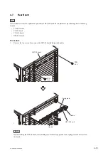
Page 29: ...may result in electric shock or damage of circuits 4 1 Tightening Torque When tightening screws used in this unit be sure to use a torque driver and tighten screws to the specified tightening torque Tightening torque PSW 3x6 0 80 0 12 N m PSW 3x30 0 80 0 12 N m M3 Shoulder screw 0 80 0 12 N m Tip When using the torque driver with the notation of cN m interpret it as follows Example 0 8 N m 80 cN m...

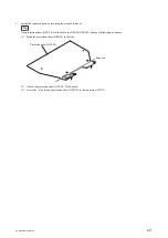
Page 30: ...ll the harness 2 Open the clamper 3 Remove the harness from the clamper and then remove the front panel Front panel Harness Connector Clamper Screw with drop safe Harness guide Harness Harness Connector Connector Clamper Harness guide Precaution during installation 4 Install the removed parts by reversing the steps of removal Note When installing the front panel pass the harness to the clamper XVS...

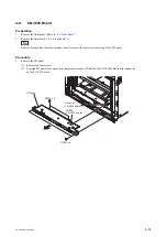
Page 31: ...Procedure 1 Open the lever and remove the switching regulator Switching regulator Power switch Lever Installing Procedure 2 While the lever is opened as shown in the illustration push the switching regulator until it stops 3 Close the lever Switching regulator Lever Lever XVS 8000 C XVS 8000 4 3 ...

Page 32: ...handle PSW3x 6 Fan holder assembly A Fan holder assembly A Fan holder assembly B Fan name Imprinting mark Handle Label Note When attaching the fan holder assemblies match the fan name on the label and the convex portions of CPU socket with the imprinting mark of the main unit 2 Install the removed parts by reversing the steps of removal 4 4 2 DC Fan Fan Holder assembly A Preparation 1 Remove the f...

Page 33: ...fan 120 square thin type CN004 b PSW3 x 30 b PSW3 x 30 a PSW3 x 30 Label Label CN002 CN 3824 board Clamper Hole of the chassis Harnesses DC fan 120 square Thick type DC fan 120 square Thin type Note When attaching the DC fan pay attention to the position of label and harness 7 Install the removed parts by reversing the steps of removal 4 4 3 DC Fan Fan Holder assembly B Preparation 1 Remove the fa...

Page 34: ...ews b 6 Pull out the harness from the hole then remove the DC fan 80 square b PSW3 x 30 b PSW3 x 30 a PSW3 x 30 a PSW3 x 30 CN003 DC fan 120 square Thick type Label CN002 DC fan 80 square CN 3824 board Clamper Hole of the chassis Label Harnesses Note When attaching the DC fan pay attention to the position of label and harness 7 Install the removed parts by reversing the steps of removal XVS 8000 C...

Page 35: ... Holder assembly A 4 4 3 DC Fan Fan Holder assembly B Procedure 1 Remove the two shoulder screws then remove the CN 3824 board CN 3824 board M3 Shoulder screw Note When installing the CN 3824 board confirm that it remove after tightened the two shoulder screws 2 Install the removed parts by reversing the steps of removal XVS 8000 C XVS 8000 4 7 ...

Page 36: ...29A board XPT 38 board Preparation 1 Remove the front panel Refer to 4 2 Front Panel Removing Procedure 1 Push the unlock buttons 1 open the eject levers 2 2 Remove the MIX 57 board 1 1 2 2 MIX 57 board Eject lever Eject lever A Unlock button Unlock button A Installing Procedure 3 While the eject levers are opened as shown in the illustration insert the MIX 57 board into the board guide XVS 8000 C...

Page 37: ... position 1 And push the eject levers 2 until the unlock buttons pop out 3 1 1 3 2 3 2 A A Board guide MIX 57 board MIX 57 board Eject lever Eject levers Eject lever Unlock button Unlock button 5 Install the removed parts by reversing the steps of removal XVS 8000 C XVS 8000 4 9 ...

Page 38: ...oard CNI 43 board CNO 43 board NET 28A board Procedure 1 Remove the two screws then remove the NET 28 board holding the handles NET 28 board PSW 3 x 6 PSW 3 x 6 Spring plate NET 28 board Handle Handle Note When installing the NET 28 board insert making sure the board s upper and lower spring plates do not catch on the board XVS 8000 C XVS 8000 4 10 ...

Page 39: ...28 is attached to the NET 28 NET 28A board as following procedures 1 Bend the protection sheet NET 28 to the line Protection sheet NET 28 Bend line 2 Attach the protection sheet NET 28 to the board 3 Cover the a portion of protection sheet NET 28 to the connector CND1 XVS 8000 C XVS 8000 4 11 ...

Page 40: ...ion sheet NET 28 to the clearance between heatsink of IC301 and the board Connector CND1 a b Heatsink of IC301 Protection sheet NET 28 Protection sheet NET 28 NET 28 NET 28A board Protection sheet NET 28 A side XVS 8000 C XVS 8000 4 12 ...

Page 41: ...ess the two push pins from the board of A side push them out in the B side of the board 7 Insert the two push pins of board to the two holes of the protection sheet NET 28 Long part of protection sheet NET 28 Panel Push pin Push pin B side Protection sheet NET 28 NET 28 NET 28A board XVS 8000 C XVS 8000 4 13 ...

Page 42: ...ards as needed to easily remove the screws for removing of the SW panel Procedure 1 Remove the SW panel 1 Remove the four screws 2 Draw the SW panel to the arrow disconnect the connector CN005 on the CN 3825 board from the connector on the CN 3826 board PSW3 x 6 SW panel CN005 CN 3825 board Connector CN 3826 board PSW3 x 6 XVS 8000 C XVS 8000 4 14 ...

Page 43: ...s from the four connectors CN001 CN02 CN003 CN004 on the CN 3825 board 3 Remove the three screws then remove the CN 3825 board PSW3 x 6 Harness Harness Harness CN001 CN003 CN004 CN002 Clamper CN 3825 board Clamper Clamper Clamper 3 Install the removed parts by reversing the steps of removal XVS 8000 C XVS 8000 4 15 ...

Page 44: ...needed to easily remove the screws for removing of the SW panel 3 Remove the SW panel Refer to 4 8 CN 3825 Board Procedure 1 Remove the screw then remove the CN 3826 board PSW3 x 6 CN 3826 board Note Tighten the screw after install the SW panel Refer to 4 8 CN 3825 Board 2 Install the removed parts by reversing the steps of removal XVS 8000 C XVS 8000 4 16 ...

Page 45: ...Section 5 Maintenance Menu This section will be described soon XVS 8000 C XVS 8000 5 1 ...

Page 46: ......

Page 47: ...IN160 XVS 8000 input signals and the internal reentry signal are input to the serial crosspoint circuit on the XPT 38 board and are then sent to the M E block output processor block frame memory block DME block and format convertor block through the matrix Color background circuit A color BKGD generator circuit for 4 channels 1 channel for 4K is provided to output the generated Color BKGD signal t...

Page 48: ... SDI signal and sends the SDI signal to the cross point block Key process circuit IC401 402 Based on the signals sent from the SDI input circuit signals sent through the mixer and signals sent from the wipe signal generator the key process circuit performs key processing for the Luminance Key Linear Key Chroma key etc and mask processing and then sends processed signals to the mixer Wipe signal ge...

Page 49: ...Resizer circuit IC301 302 This block applies resizer effects to the signal sent from the mixer block and sends the signal to which resizer effects were applied to the mixer block XVS 8000 C XVS 8000 6 3 ...

Page 50: ...SLOT2 to the two DVP 53A boards AUX KEY circuit IC002 IC003 Out processes including CCR video process blanking SafeTitle superimposition and output phase adjustment and the AUX KEY process are added to the SDI signals sent from the serial cross point circuit and then processed SDI signals are sent to the CNO 43 board The OUT 38A board contains four AUX KEY circuits 6 3 2 CNI 43 Board XKS S8110 The...

Page 51: ...This board is provided with the Gigabit Ethernet signal connector to be connected to the CA 92 board and the reference signal buffer circuit XVS 8000 C XVS 8000 6 5 ...

Page 52: ...nnected to the hub Generating a clock signal and a timing signal in synchronization with the reference signal Clock Generation IC2001 generates HSOUT VSOUT and OEOUT signals from the REF_IN signal that is input from the MB 1223 board IC2003 generates VCLK signals for HD and SD by using these signals Clock Distribution VCLK signals generated in IC2003 and the TOF and UID signals from the CPLD IC2 a...

Page 53: ... XVS 8000 and CN 3826 Board XVS 8000 The CN 3825 board relays signals among the power switch FP 255 board and CN 3826 board The CN 3825 board also generates 5 V from 12 V supplied from the CN 3826 board and supplies 5 V power to the FP 255 board The switch S001 can be set to turn OFF the LEDs on the FP 255 board The CN 3826 board relays signals between the MB 1223 board and the CN 3825 board The C...

Page 54: ...converted to parallel signal and parallel signal is sent to NeptuneII IC1001 IC1801 IC3601 IC4401 as User IF signal The User IF signal sent from the FPGA to NeptuneII IC1001 IC1801 IC3601 IC4401 is processed for FEC LLVC Encode Decode NetworkPacketize Network synchronization in NeptuneII and the processed signal is sent to the Network PHY IC1501 IC2301 IC4101 IC4901 as XAUI signal The Network PHY ...

Page 55: ...ases FPGA reset to boot the Nios Writing installation data Installation data used in the production process is stored in the flash memory IC207 IC208 IC2807 IC2808 through the local bus connected to the CA 92 board Update Version update of the NET 28 board on the market is enabled on the web using the Ethernet port of the Net Media interface Package data including the following data is released al...

Page 56: ...nput signal or the video clip imported from the external device in the internal SSD The stored video clip is sent to the FPGA through PCIe or is exported to external devices upon instructions from the upper CPU Ethernet communication This CPU performs communication with the upper CPU to control Clip Store and also imports and exports video clip from to external devices through this Ethernet commun...

Page 57: ...CPU to the flash memory for applications and FPGA configuration data Status beacon power LED control and 7SEG LED control Monitoring board power status Control of clock generator VIDEO system IC2004 and IC2005 CPU system IC3204 IC3206 and IC3207 XVS 8000 C XVS 8000 6 11 ...

Page 58: ...converted or video processed signals to a serial signal and then outputs the serial signal from CNP1 CNL1 and CNE1 as SDI signal for up to 20 channels DDR control The DDR memory is used for video signal format conversion The DDR memory consists of four 4GB_DIMM devices Local_Bus communication This FPGA performs communication of command and status information with the upper CPU through the Local_Bu...

Page 59: ...INTPU block and sends the return video key signals processed in the FINTPU block and the AINTPL block to the PVMIX block The PVMIX block has the following main functions Border Crop Beveled Edge Video Modify including Posterization Solarization and Mosaic Input Freeze Mask key generation Recursive FINTPU block IC7 IC8 This block first performs horizontal Defocus Blur and Filtering processing Antia...

Page 60: ...rmed Then the interpolated video key signals of the FINTPU block are received for vertical interpolation The video key signals are then sent to the PVMIX block where Lighting synthesis is applied to the video key signals by the Light key generated in the AINTPL block The AINTPL block has the following main functions 3D Linear Transform Non linear Interpolation Lighting Field Frame Conversion VMIX ...

Page 61: ...r from those used for the unit These are because of parts common ality and improvement 3 Stock of Parts Parts marked with o at SP Supply Code column of the spare parts list may not be stocked Therefore the delivery date will be delayed 1 安全重要部品 警告 印のついた部品は安全性を維持するために重 要な部品です したがって 交換する時は必ず 指定の部品を使ってください 2 部品の共通化 ソニーから供給する補修用部品は セットに使われ ているものと異なることがあります これは部品の共通化 改良等によるものです 3 部品の在庫 部品表の SP Supply c...

Page 62: ...OOT ASSY 4 1 474 652 11 s REGULATOR SWITCHING 5 1 971 159 12 s HARNESS SUB CN3825 FP 6 3 172 089 01 o HANDLE 7 3 650 537 01 s WASHER 8 3 655 653 01 s BAND TAITON BINDING 9 3 994 237 01 s SPACER No Part No SP Description 10 4 170 582 02 s BRACKET PANEL 11 4 183 472 01 s ESCUTCHEON 12 4 549 457 11 s PANEL SIU BAR 13 4 586 400 01 s CUSHION FRONT PSU 14 4 586 401 01 s LIGHT GUIDE 15 4 586 402 01 s HOL...

Page 63: ...cription 20 4 812 134 11 s RIVET DIA 3 5 NYLON 7 628 253 05 s SCREW PS 2X4 7 682 562 04 s SCREW B 4X10 7 682 647 01 s SCREW PS 3X6 7 682 947 01 s SCREW PSW 3X6 Front Panel and Switching Regulator XVS 8000 C XVS 8000 7 3 ...

Page 64: ...UIT BOARD CN 3826 103 1 798 563 11 s SWITCH POWER 104 1 971 158 11 s HARNESS SUB CN3825 SW 105 3 701 443 21 s WASHER 5 DIA 106 3 733 690 01 s B 4X6 CU NI 107 4 098 036 01 s SADDLE WIRE A 108 4 586 452 01 s PANEL SW 109 4 586 453 01 s COVER SWITCH 110 4 586 454 01 s LABEL SLOT NUMBER 111 4 586 456 01 s PLATE R LOCK 112 4 586 457 01 s PLATE L LOCK 113 4 586 460 01 s CUSHION HANDLE VIBRATION PROOF 11...

Page 65: ...A 250V 203 1 842 404 11 s AC INLET SCREW 3P FASTEN 204 1 971 160 11 s HARNESS SUB NF MB 205 1 971 161 11 s HARNESS SUB INLET NF 206 1 971 162 11 s HARNESS SUB INLET BREAKER 207 2 990 241 02 s HOLDER A PLUG 208 3 172 089 01 o HANDLE 209 3 725 295 21 s SCREW B3 210 4 586 455 01 s LABEL CN SLOT No Part No SP Description 211 4 586 462 01 s PANEL REAR 7 682 947 01 s SCREW PSW 3X6 7 682 950 01 s SCREW P...

Page 66: ... MOUNTED CIRCUIT BOARD CN 3824 302 X 2592 777 1 s HOLDER ASSY FAN PC BOARD 303 1 787 908 12 s FAN DC 80 SQUARE 304 1 855 201 11 s FAN DC 120 SQUARE 305 1 855 435 11 s FAN DC 120 SQUARE 306 2 102 434 01 s SCREW M3 ECO STEP 307 3 172 089 01 o HANDLE 7 682 947 01 s SCREW PSW 3X6 No Part No SP Description 7 682 955 01 s SCREW PSW 3X30 XVS 8000 C XVS 8000 7 6 ...

Page 67: ... CIRCUIT BOARD CA 92 404 X 2583 078 2 s BOARD LEVER GF ASSY 405 1 857 571 12 s PC BOARD MOUNT CPU DP MODULE 406 4 187 619 01 s SHEET RADIATION 25X25X2 407 4 812 134 11 s RIVET DIA 3 5 NYLON 408 6 714 073 01 s IC 88E1118R A0 NNC2C000 409 4 545 123 01 s LABEL 10A FUSE 7 626 320 61 s PIN SPRING 3X18 7 682 549 09 s SCREW B 3X10 7 682 947 01 s SCREW PSW 3X6 7 682 951 01 s SCREW PSW 3X14 No Part No SP D...

Page 68: ...6 01 s CUSHION 507 4 143 557 01 s SPRING COMPRESSION 508 4 143 559 01 s PIN PUSH 509 4 183 612 01 s SHEET WIND SHIELDING 510 4 187 619 01 s SHEET RADIATION 25X25X2 511 4 187 619 01 s SHEET RADIATION 25X25X2 512 4 187 620 01 s SHEET RADIATION 33X33X1 5 513 4 586 492 01 s INSULATING SHEET PWB 514 4 812 134 11 s RIVET DIA 3 5 NYLON No Part No SP Description 515 6 714 073 01 s IC 88E1118R A0 NNC2C000 ...

Page 69: ...S 603 X 2583 078 2 s BOARD LEVER GF ASSY 604 1 857 571 12 s PC BOARD MOUNT CPU DP MODULE 605 4 143 559 01 s PIN PUSH 606 4 187 619 01 s SHEET RADIATION 25X25X2 607 4 586 519 01 s SHEET 1 28X28 RADIATION 608 4 812 134 11 s RIVET DIA 3 5 NYLON 609 6 714 073 01 s IC 88E1118R A0 NNC2C000 610 4 545 123 01 s LABEL 10A FUSE 7 626 320 61 s PIN SPRING 3X18 7 682 549 09 s SCREW B 3X10 7 682 947 01 s SCREW P...

Page 70: ... 702 A 2084 271 A s MOUNTED CIRCUIT BOARD OUT 38 for OUT 38 board 703 X 2583 078 2 s BOARD LEVER GF ASSY 704 3 561 426 01 s CUSHION 705 4 143 557 01 s SPRING COMPRESSION 706 4 143 559 01 s PIN PUSH 707 4 187 620 01 s SHEET RADIATION 33X33X1 5 708 4 545 123 01 s LABEL 10A FUSE 7 626 320 61 s PIN SPRING 3X18 7 682 947 01 s SCREW PSW 3X6 7 682 951 01 s SCREW PSW 3X14 No Part No SP Description 7 685 1...

Page 71: ...83 A s ASSY PBS 803 X 2583 078 2 s BOARD LEVER GF ASSY 804 1 853 478 11 s LITHIUM BATTERY BR2032 TYPE for VPR 129 board 805 4 143 557 01 s SPRING COMPRESSION 806 4 143 559 01 s PIN PUSH 807 4 586 519 01 s SHEET 1 28X28 RADIATION No Part No SP Description 808 4 812 134 11 s RIVET DIA 3 5 NYLON for VPR 129 board 809 4 545 123 01 s LABEL 10A FUSE 810 6 722 392 01 s IC HMT425S6CFR6A PBN0 for VPR 129 b...

Page 72: ... 722 796 01 s IC THNSNJ480PCSZ4PDET for VPR 129 board 7 626 320 61 s PIN SPRING 3X18 7 682 947 01 s SCREW PSW 3X6 7 682 951 01 s SCREW PSW 3X14 7 685 145 14 s SCREW P 3X6 TYPE2 NON SLIT VPR 129 VPR 129A Board XVS 8000 C XVS 8000 7 12 ...

Page 73: ... SP Description 901 A 1771 683 A s ASSY PBS 902 A 1771 684 A s BOARD LEVER F ASSY 903 A 2084 268 A s MOUNTED CIRCUIT BOARD XPT 38 904 3 942 866 02 s NUT M3 3X0 5 NYLON 905 4 143 559 01 s PIN PUSH 906 4 187 620 01 s SHEET RADIATION 33X33X1 5 907 4 545 123 01 s LABEL 10A FUSE 7 626 320 61 s PIN SPRING 3X18 7 682 947 01 s SCREW PSW 3X6 7 682 951 01 s SCREW PSW 3X14 XVS 8000 C XVS 8000 7 13 ...

Page 74: ... 1004 1005 No Part No SP Description 1001 A 2082 225 A s MOUNTED CIRCUIT BOARD CN 3807 1002 2 655 586 01 s SCREW B M2 6 EG 1003 3 172 089 01 o HANDLE 1004 3 637 901 02 s SCREW M2 6X5 1005 4 586 498 01 s PANEL CN 3807 7 621 759 45 s PSW 2 6X6 XVS 8000 C XVS 8000 7 14 ...

Page 75: ...Rear view CNI 43 CNO 43 SLOT No 13 SLOT No 14 SLOT No 15 SLOT No 16 SLOT No 17 1101 1101 1102 1103 No Part No SP Description 1101 3 172 089 01 o HANDLE 1102 3 637 901 02 s SCREW M2 6X5 1103 4 586 501 01 s PANEL CNI CNO IN CNI 43 IN for CNI 43 board 4 586 501 11 s PANEL CNI CNO OUT CNO 43 OUT for CNO 43 board XVS 8000 C XVS 8000 7 15 ...

Page 76: ...1204 1204 1203 1206 1207 1206 No Part No SP Description 1201 X 2592 916 1 s PANEL NET 28 IN ASSY for NET 28 board X 2592 917 1 s PANEL NET 28 OUT ASSY for NET 28A board 3 172 089 01 o HANDLE 1203 4 143 557 01 s SPRING COMPRESSION 1204 4 143 559 01 s PIN PUSH 1205 4 586 499 01 s SHEET NET 28 PROTECTION No Part No SP Description 1206 4 586 519 01 s SHEET 1 28X28 RADIATION 1207 4 545 123 01 s LABEL 1...

Page 77: ...ied Accessories Q ty Part No SP Description 1pc 1 695 542 21 s TERMINATOR 75 1pc 4 589 310 01 s OPERATION MANUAL 1pc 4 589 402 02 s CD ROM 8pcs 7 682 562 04 s SCREW B 4X10 8pcs 7 682 962 01 s SCREW PSW 4X10 XVS 8000 C XVS 8000 7 17 ...

Page 78: ......

Page 79: ... 2 BGDCOL 24 OUT 4 DMEUTL OUT 38A 8 AUX KEY 24 OUT AuxKey 24 OUT 4 OUT XPT 38 290x290 8 MV 20 128 160 160 NMI 4k 40in 264 CNO NET CNO NET CNO NET CNO NET CNO NET 16 16 16 16 12 8 BLANK BLANK CNI NET CNI NET CNI NET CNI NET CNI NET CNI NET CNI NET CNI NET CNI NET CNI NET CNO NET CNO NET CNO NET CNO NET CNO NET CN 3807 CNI NET CNI NET CNI NET CNI NET CNI NET CNI NET CNI NET CNI NET CNI NET CNI NET 1...

Page 80: ...7 0 MB 1223 8bit SWITCH GROUP UNIT ID LVDS TOFO 7 0 UID 3 0 VD 11 0 SERIAL_CLK SERIAL_LD SERIAL_DATA OEOUT VSOUT HSOUT TOF1 TOF2 TOF3 NO REF NO ALGN NO LOCK INT LMH1983 IC2003 CLK3 CLK2 CLK1 SEL 2x2 LVDS SEL 2x2 BUF SD VCLK_HD 1 0 VCLK_SD 1 0 BUF HD HF_CK0 HF_CK1 VCLK 12 0 VCLK_R 15 0 VCLK2_R 15 0 VCLK_HD CLKSEL 3 2 CLKSEL 1 0 VCLK_SD MB 1223 GbE HUB0 IC1401 Transformer Transformer Transformer Tra...

Page 81: ...D1 CN101 GBE0_TRX CNL1 1 8V CN102 GBE1_TRX CNL1 1 8V NETWORK A NETWORK B REF INPUT EEPROM MB_3 3V IC001 EEPROM MB_3 3V IC002 MB_SDA MB_SCL CNB1 I2C BUS 1 8V Regulator IC003 1 8V DC 12V CNB1 MB_3 3V CNB1 XVS 8000 C XVS 8000 8 3 ...

Page 82: ...GND 12V SCL SDA EN A0 A1 A2 INH 5V SCL SDA EN A0 A1 A2 INH 5V SCL SDA EN A0 A1 A2 INH 5V SCL SDA A2 INH EN 5V A1 A0 MB 1223 CN001 PS1_I2C_GA2 PS1_INHIBIT PS1_ENABLE PS1_ 5V_STANDBY PS1_I2C_GA1 PS1_I2C_GA0 FP_CTRL1 12V PS4_ENABLE PS4_I2C_GA0 PS4_I2C_GA1 PS4_I2C_GA2 PS4_INHIBIT PS4_ 5V_STANDBY PS3_ENABLE PS3_I2C_GA0 PS3_I2C_GA1 PS3_I2C_GA2 PS3_INHIBIT PS3_ 5V_STANDBY PS2_ENABLE PS2_I2C_GA0 PS2_I2C_G...

Page 83: ...Cable Equalizer IC307 IN17 Reclock Distributor IN18AP N IN18BP N CNF1 CNF1 IC802 Cable Equalizer IN18 Reclock Distributor IN19AP N IN19BP N CNF1 CNF1 IC803 Cable Equalizer IN19 Reclock Distributor IN20AP N IN20BP N CNF1 CNF1 IC804 Cable Equalizer IN20 IC308 IC309 IC310 Reclocker Control Reclocker Control IC101 SLOT_No0 7 Regulator DC 3 3V D 1 2V Converter Dc to DC 3 3V IC002 Converter Dc to DC 2 5...

Page 84: ... Driver IC302 OUT10 OUT11P N CNF1 Cable Driver IC303 OUT11 OUT12P N CNF1 Cable Driver IC304 OUT12 OUT13P N CNF1 Cable Driver IC401 OUT13 OUT14P N CNF1 Cable Driver IC402 OUT14 OUT15P N CNF1 Cable Driver IC403 OUT15 OUT16P N CNF1 Cable Driver IC404 OUT16 OUT17P N CNF1 Cable Driver IC501 OUT17 OUT18P N CNF1 Cable Driver OUT18 OUT19P N CNF1 Cable Driver OUT19 OUT20P N CNF1 Cable Driver OUT20 IC502 IC...

Page 85: ..._UTIL22C Y S P SDI IN_ TBC SEL CNG1 1 ME_EXT_DMEA ME_EXT_DMEB ME_UTIL1A ME_UTIL1B ME_UTIL2A ME_UTIL2B ME_UTIL3A ME_UTIL3B EXT_DMEC_A EXT_DMEY_A UTIL1C_A UTIL1Y_A UTIL2C_A UTIL2Y_A UTIL3C_A UTIL3Y_A EXT_DMEC_B EXT_DMEY_B UTIL1C_B UTIL1Y_B UTIL2C_B UTIL2Y_B UTIL3C_B UTIL3Y_B EXT_DMEC_A EXT_DMEY_A UTIL1C_A UTIL1Y_A UTIL2C_A UTIL2Y_A UTIL3C_A UTIL3Y_A EXT_DMEC_B EXT_DMEY_B UTIL1C_B UTIL1Y_B UTIL2C_B U...

Page 86: ... IC D719 STATUS BECON POWER PLL UNLOCK 7Seg LED D701 716 REG 1 8V 0 9A IC2902 CL2900 0 9V_REF3 IC2900 2901 3000 3001 REG 1 8V 0 9A IC2702 CL2700 0 9V_REF2 IC2700 2701 2800 2801 REG 1 8V 0 9A IC2502 CL2500 0 9V_REF1 IC2500 2501 2600 2601 REG 1 8V 0 9A IC2302 CL2300 0 9V_REF0 IC2300 2301 2400 2401 REG 1 8V 0 9A IC2102 CL2100 0 9V_REF W IC2100 2101 2200 2201 VCLK 1 CNB1 12V F001 15A 65V HotSwap Prote...

Page 87: ...er IF8 20 1 User IF5 20 1 REF GEN S P XAUI P0 Lane 4 1 XAUI P1 Lane 4 1 XAUI P0 Lane 4 1 XAUI P1 Lane 4 1 IC4101 PHY C IC4901 PHY D J4201 J4202 J5001 J5002 27M 74M VCO391 X4001 VC4002 VC4001 TG Block 148M 27M 74M 148M IC301 FPGA REFCLK_CH1 4_P N XCVRCLK_CH1 4_P N REFCLK_CH5 8_P N XCVRCLK_CH5 8_P N IC5401 Clock Matrix FPGA A_VCLK74M P N FPGA A_VCLK148M P N FPGA A_VCLK27M P N FPGA A_VCLK148 5M P N I...

Page 88: ...IC1501 IC2302 1 2V P1 DDcon IC2606 12V 1 8V 1 8V P2 To IC1501 IC2302 1 8V P1 DDcon IC2609 3 3V 2 5V 2 5V 1 To IC301 LDO IC2609 3 3V 2 5V 2 5V FA1 To IC301 LDO IC2605 3 3V 2 2V 2 2V P2 To IC1501 IC2302 2 2V P1 DDcon IC2607 3 3V 1 8V 1 8V 1 To IC301 LDO IC2609 3 3V 2 5V 1 5V FA1 To IC301 DDcon IC2705 12V 1 1V 1 1V ND2 1 1V ND1 1 1V NA2 1 1V NA1 To IC1001 IC1801 PG_1 1V NEP2 LDO IC2705 3 3V 2 5V DDco...

Page 89: ...LD PON_RST_FPGA PON_RST_NEP2 IC102 Tranceiver CNB1 EXTBUS2_AD 15 0 SLOT NO 7 0 IC105 RS 485_Rx P N RS 485_Tx P N DE DI RO IC2801 CADEC CN2801 JTAG CN2802 JTAG J4201 J4202 IC4101 PHY C IC4104 Flash MDIO IC3601 NEP2 A CN3801 232C SPI IC3805 EEPROM IC3806 Flash IC3701 DDR3 IC3807 eMMC I2C SPI A16 DQ16 8bit VCO391 X4001 VC4002 VC4001 TG Block HIF 31 0 J5001 J5002 IC4901 PHY D IC4904 Flash MDIO IC4401 ...

Page 90: ...CNG1 OUT05 08INA CNE1 OUT09 12INA CND1 DSKIN_FILL SRC1 3 SDI RX IN TBC CCR KEYER TX SDI OUTTBC OUTTBC OUTTBC AUXMIX AUXMIX AUXMIX SEL OUTTBC OUTTBC RX SDI SEL CASMIX SEL CURSOR SDI TX OUT1 OUT2 IC002 IC003 VPR IC005 RX SDI RX SDI TX SDI TX SDI OUT 38 OUT 38A NoMount Mount SDRAM DDR2 IC4401 CNP1 CNN1 CNL1 CNP1 CNK1 CNG1 CNE1 CNP1 OUT01 04 OUT05 08 OUT09 12 DSK_OUT1 3 OUT13 16 OUT17 20 OUT21 24 DSK_...

Page 91: ...02 D301 3 3V F103 TP103 DC DC CONV IC103 D302 2 5V F104 TP104 DC DC CONV IC104 D303 1 8V F105 TP105 DC DC CONV IC105 D305 1 1V 1 F106 TP106 DC DC CONV IC106 D306 1 1V 2 F107 TP107 DC DC CONV IC107 D310 0 9V F108 TP108 DC DC CONV IC108 D308 1 1V A 3 3V LINEAR REGULATOR IC201 TP201 1 5V A1 LINEAR REGULATOR IC202 TP202 1 5V A2 LINEAR REGULATOR IC205 TP204 1 2V LINEAR REGULATOR IC206 TP205 1 5V A3 LIN...

Page 92: ...3203 BUF IC2501 IC2052 D2501 D2516 CADEC IC2 DIR OE CNB1 IC2302 VD IC2303 FD RESET SLOT No IC2004 CLOCK CLEANER IC2005 CLOCK CLEANER CC_CTRL 27M 74M CC_CTRL 74M IC2402 JTAG D2201 D2204 D2202 D2203 EPR2 CN2401 BUF BUF BUF STATUS BECON POWER INIT_ERR S2303 D2402 CONF_ERR RESET GEN S3301 RE_CONFIG CNP1 CNL1 CNE1 SDI OUT CH1 CH8 SDI OUT CH9 CH16 SDI OUT CH17 CH20 CLK_25M DC DC_PG CPU_LCLK CPU_LAD CPU_...

Page 93: ...V CPU1 1 0V CPU2 DC_DET IC1333 1 2 EN 1 0V_CPU_PG to IC2 F1603 10A 125V DC DC 3 3V IC1602 3 3V CPU 3 3V_2 3 3V_PG to IC2 DC DC 3 3V IC1702 3 3V C DC DC 1 2V IC1701 1 2V C CADEC_PG to IC2 DC DC 1 5V IC1604 5V 5 0V_PG to IC2 F1402 5A 125V DC DC 1 35V IC1404 1 35V DC_DET IC1333 2 2 EN 1 35V_PG to IC2 F1403 10A 125V DC DC 2 5V IC1405 2 5V 2 5V_PG to IC2 DC DC 3 3V IC1403 3 0V F 3 0V_F_PG to IC2 DC DC ...

Page 94: ...OCK SYS_RESET CONFIG CONF_DONE 125M_REFCLK from IC3203 BUF IC2501 IC2052 D2501 D2516 CADEC IC2 DIR OE CNB1 IC2302 VD IC2303 FD RESET SLOT No IC2004 CLOCK CLEANER IC2005 CLOCK CLEANER CC_CTRL 27M 74M CC_CTRL 74M IC2402 JTAG D2201 D2204 D2202 D2203 EPR2 CN2401 BUF BUF BUF STATUS BECON POWER INIT_ERR S2303 D2402 CONF_ERR RESET GEN S3301 RE_CONFIG CNP1 CNL1 CNE1 SDI OUT CH1 CH8 SDI OUT CH9 CH16 SDI OU...

Page 95: ...CADEC_PG to IC2 F1402 5A 125V DC DC 1 35V IC1404 1 35V DC_DET IC1333 2 2 EN 1 35V_PG to IC2 F1403 10A 125V DC DC 2 5V IC1405 2 5V 2 5V_PG to IC2 DC DC 3 3V IC1403 3 0V F 3 0V_F_PG to IC2 DC DC 3 3V IC1402 3 3V F 3 3V_F_PG to IC2 F1501 10A 125V 1 5V FPGA IC1501 F1502 10A 125V 1 0V FPGA IC1405 1 0V 1 0V_PG to IC2 1 5V 1 5V_PG to IC2 PG 25MHz X tal X3202 CLOCK BUF IC3203 125MHz X tal X3204 125MHz REF...

Page 96: ...ut Process P S 4 4 4 Internal SG Color BG Multi Viewer Out1 4 Multi Viewer Out5 8 CNT12 1 IC002 1 3 290x290 Crosspoint IC DDR3 IC3601 IC3602 IC3701 IC3702 CNT01 12 1 CNT01 12 1 CNT01 12 1 248 20 4 Internal Video Source CNOUT FCOUT1 20 No Use 126 CNT01 12 Re Entry Input 1 160 CNT01 12 Primary Input 1 4 VIDEO BLOCK 1 REFER TO SCHEMATIC IC003 1 5 MV FPGA XVS 8000 C XVS 8000 8 18 ...

Page 97: ...O DC DC CONV F402 IC402 TP402 D806 1 2V_XPT_IO DC DC CONV F403 IC403 TP403 D804 1 8V_XPT_IO DC DC CONV F501 IC501 TP502 D803 2 5V DC DC CONV F601 IC601 TP601 D810 0 95V DC DC CONV F602 IC602 TP602 D805 1 8V DC DC CONV F603 IC603 TP603 D807 1 5V DC DC CONV F701 IC701 TP701 D809 1 0V DC DC CONV F702 IC702 TP702 D808 1 2V DC DC CONV F502 IC502 TP503 D801 3 3V DC DC CONV TB501 IC503 TP501 1 2V_CADEC C...

Page 98: ...NT15 CNT16 CNT17 CNT18 CNT19 CNT20 CNT21 CNT22 CNT23 CNT24 MB 1223 Board 1 Daughter Board name Main Board XPT 38 Board Caution Each Daughter Board has a few fuse except 1 2 CNP104 CNP105 CNP111 CNB114 CNC114 CNT01 CNT02 CNT03 CNT04 CNT05 CNT06 CNT07 CNT08 CNT09 CNT10 CNT11 CNT12 XPT 38 Board CNE115 CNL115 CNC115 CNB115 CNP115 VPR 129A Board XKS 8460 OUT 38 Board CNC116 CNB116 CND116 CNE116 CNG116 ...

Page 99: ...Y FAN 6 C6 CN4 PS4_INHIBIT D1 SENSE CN4 PS4_ENABLE D2 CN4 D3 PS4_I2C_SDA CN4 FAN 1 FAN 2 FAN 3 PS4_I2C_GA2 FAN 5 D4 FAN 4 FAN 6 CN4 Left side FRONT D6 REAR CN4 PS4_FAULT 12V FG FG FG FG 12V POWER SUPPLY UNIT D APS 406 FAN FAN Green LED AC OK Green LED DC OK Orange LED FAULT A1 B1 C1 D1 5A 125V 1 D5 FAN 5 CN001 CN001 CN001 PS1_EXIST A8 B8 C8 PS1_ENABLE PS1_I2C_GA2 12V GND CN13 12V D8 E8 PS1_I2C_GA1...

Page 100: ......

Page 101: ......

Page 102: ...XVS 8000 C SY XVS 8000 SY XVS 8000 CN J E 9 878 693 01 Sony Corporation Printed in Japan 2016 1 08 2016 ...

Reviews: