background image

Cont

ro

l

22

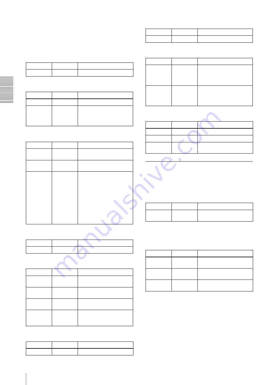
Actual control can be carried out by setting registers 
from F0F00800 onward.
ddd indicates the control value expressed as a 12 bit 
hexadecimal number.
xxx indicates that any setting made will be ignored.

Brightness control

Gamma control

Shutter (exposure time) control

Gain control

Trigger control

Trigger Delay control

Pan control

GPIO control

Strobe control

The formula for absolute value 
shutter control register address

Absolute value shutter control CSR offset 
address

The register address for absolute value shutter control is 
given by the following formula.

F00 003C025Ch 

× 

4 = F0F00970h

The data is indicated by 32-bit floating-point format. 
3727C5AC is 0.00001, and 41800000 is 1.

Address

Data

F0F00800

82000ddd

Adjusts the black level.

Address

Data

F0F00818

82000000

Sets Gamma to OFF.

82000mmn

n: 1h to Fh (1 to 16) gamma 
curve n×0.1 equivalent
mm: 00h to FFh (0 to 255) 
gamma curve starting position

Address

Data

F0F0081C

82000ddd

Controls shutter using the 
manually set relative value.

C2000xxx

Controls shutter using the 
manually set absolute value.

F0F00978h
(To obtain 
this address, 
see “The 
formula for 
absolute 
value shutter 
control 
register 
address” on 
page 22.
)

Determines 
the optional 
value using 
the 32-bit 
floating-
point format.

After F0F0081C has been set 
to the absolute value control, 
set the exposure time using 
this register.

Address

Data

F0F00820

82000ddd

Set Gain manually.

Address

Data

F0F00830

82000000

Sets to Hardware Trigger 
Mode0.

82010000

Sets to Hardware Trigger 
Mode1.

82E00000

Sets to Software Trigger 
Mode0.

F0F0062C

80000000

Outputs a software trigger. 
Automatically resets to 0 when 
exposure ends.

Address

Data

F0F00834

82000ddd

Sets Trigger Delay.

Address

Data

F0F00884

82000ddd

Sets Pan manually.

Address

Data

F0F20400

0000000d

Outputs a signal to the output 
port. 
bit31: GPO1
bit30: GPO2 

F0F20404

Reads out the status of the 
input port. 
bit31: GPI1
bit30: GPI2

Address

Data

F0F20200

80000000

A strobe signal is not output.

82000000

Outputs an exposure signal.

82dddwww

ddd = delay, www = signal 
width, unit = µs.

Address

Data

F0F0071C

003C025C

Absolute value shutter control 
CSR offset.

Address

Data

F0F00970

3727C5AC

Absolute value shutter control 
minimum value. (ReadOnly)

F0F00974

41800000

Absolute value shutter control 
maximum value. (ReadOnly)

F0F00978

Absolute value shutter control 
setting value.

Summary of Contents for XCD-MV6

Page 1: ...Technical Manual A DVH 100 11 1 Digital Video Camera Module 2010 Sony Corporation XCD MV6 ...

Page 2: ...ConfigurationROM 17 Control Base Address 19 Inquiring about Supported Video Modes 19 Video Mode Settings S800 S1600 19 Starting Stopping Video Transfer ContinuousShot 19 OneShot MultiShot and ImageBuffer 20 Control of IIDC Standard Features 21 The formula for absolute value shutter control register address 22 Control of IIDC Optional Features 23 Control of Sony s Unique Features 24 Displaying the ...

Page 3: ...on use Broadcast delivery of commands The camera settings for all the cameras connected to the same bus can be changed at the same time For example the gain or shutter speed is set to the same value on all the cameras or exposure starts on all the cameras simultaneously using a software trigger Memory Channel The memory channel allows storage of up to 15 sets of camera settings such as gain and sh...

Page 4: ...or damage to the camera or cable use the cable equipped with fixing screws 3 C mount lens commercially available Use an appropriate lens for the camera module and usage 4 Camera module interface board commercially available This is inserted in slots such as the PCI Express bus or PCI bus of the host equipment PC etc Select an IEEE1394b interface board to match your system 5 DC 700 700CE camera ada...

Page 5: ...ompatible host adapter card and IEEE1394b cable For details contact your Sony dealer In addition this equipment is exclusively for beta mode use so it is not possible to connect it to the IEEE1394a host adapter card with the IEEE1394 9P 6P cable C mount lens Host equipment PC etc IEEE1394b cable Host adaptor card XCD MV6 ...

Page 6: ...ng the camera module Locking the camera module into these holes secures the optical axis alignment For details see Dimensions on page 33 Rear 4 IEEE1394b connectors Connect an IEEE1394b camera cable not supplied to this connector 5 8 pin I O connector When power from the IEEE1394b connector is insufficient power is supplied through this connector 1 2 3 3 Pin No Signal Pin No Signal 1 TPB 6 VG 2 TP...

Page 7: ...ntil it snaps into place holding it Then tighten the fixing screws placed on both sides of the cable connector 1 IEEE1394b connector 2 Fixing screws 3 IEEE1394b camera cable not supplied Note Loose fixing screws may cause a poor connection or damage to the camera or cable Be sure to tighten the fixing screws When power supply from the IEEE1394b connector is insufficient Power can be supplied to th...

Page 8: ...a mild detergent then wipe with a dry cloth Do not apply organic solvents such as alcohol which may damage the finish Phenomena Specific to CMOS Sensors The following phenomena that may appear in images are specific to CMOS sensors They do not indicate malfunctions White flecks Although the CMOS sensors are produced with high precision technologies fine white flecks may be generated on the screen ...

Page 9: ...e to confirm the output waveform before use GPO1 2 output circuit This is a GPO1 2 output circuit diagram This is a standard CMOS level output 5 V Equipped with a protective resistor of 2 2 kΩ Be sure to confirm the output waveform before use GPI1 2 input circuit This is a GPI1 2 input circuit diagram Compatible with standard TTL level input Equipped with a protective resistor of 10 kΩ Be sure to ...

Page 10: ...ring images in response to a trigger signal that starts the exposure to match a preset timing It can also be used to capture an image using multiple cameras with the same timing This camera supports a hardware trigger input from 8 pin connectors and 2 types of software trigger set by 1394 bus command Note Switching trigger signals may cause image disturbance Be sure to take note of this before use...

Page 11: ...tput signal is assigned to the 8 pin connector This feature allows strobe equipment connected to the camera to directly emit light Output delay and width can be set for the exposure time Camera exposure time can be output without change GPIO A general purpose I O port with a 2 bit output and 2 bit input is assigned in the 8 pin connector This port is used for reading information of external switch...

Page 12: ...hronize with the 1394 bus and operate As band restrictions will be applied depending on the transmission rate configured you must configure a video mode that will allow simultaneous video transmission When long exposure mode i e when the exposure time configured is longer than the image transmission frequency pseudo binning mode or partial scan mode is configured the synchronization function will ...

Page 13: ...fer Memory Shot The camera has image buffer Memory Shot that temporarily stores an image in the frame memory inside the camera and transfers it later When multiple cameras are connected in the same bus all the cameras may not output images at the same time due to the restriction of the set transmission rate ImageBuffer Memory Shot may resolve this inconvenience When exposure starts each camera sto...

Page 14: ...ransmission rate band When using Partial scan mode set Format7 Mode0 Note By selecting Partial scan mode it is possible to set the maximum value of 752 pixels for the horizontal size of the image However because the horizontal direction increases by a factor of 64 the image data is set to 768 pixels causing 16 pixel wide completely black data to be output in the right edge of the image Although th...

Page 15: ...g OFF This features corrects shading caused by light falloff at lens edges uneven brightness and sensors This can only be selected with user settings and either the average value or the pixel level maximum value within 1 frame can be selected as the target value It would be useful to make the following distinction when generating shading correction values little noise maximum value lots of noise a...

Page 16: ...de IDs may be changed if the topology is restructured because of bus reset so only the least significant 32 address bits are shown in this Guide bbbbbbbb bbnnnnnn 11111111 11111111 11110000 11110000 00000000 00000000 NodeID BusID Must be 1 Address used by the camera Address Resister F0000000 Base address F0000400 ConfigROM area F0F00000 Base address for camera commands F0F00000 CameraInitialize F0...

Page 17: ...conforms to IIDC Standards Version 1 3 The offset address of UnitDependentInfo is required to be 430h 000001h 4 434h Offset 0 7 8 15 16 23 24 31 Bus Info Block 400h 04 21 ROM CRC 404h 31 33 39 34 408h 20 FF 92 14 40ch 08 00 46 10 NodeVendorID ChipID Hi 410h 00 37 1A 96 Chip ID Lo Root Directory 414h 0003 CRC 418h 03 08 00 46 ModuleVendorID 41ch 0C 00 83 C0 420h D1 00 00 01 UnitDirectoryOffset Offs...

Page 18: ...e_info_0 is the firmware version Vendor_unique_info_1 is the hardware version Vendor_unique_info_2 is the link version Vendor_unique_info_3 is the serial number of the camera VendorNameLeaf For offset address 464h the length of the VendorNameLeaf is 3 Quadlets The subsequent 8 bytes are fixed at 00 After that the four characters for SONY are entered ModelNameLeaf For offset address 474h the length...

Page 19: ...f 800 Mbps and isochronous channel 0 are used in these examples Normally set the isochronous transfer speed to 800 Mbps or 1600 Mbps When multiple cameras are used simultaneously set different isochronous channels for each Starting Stopping Video Transfer ContinuousShot In the device driver after the preparations for receiving isochronous data are made video transfer starts when the following comm...

Page 20: ...g command is read the maximum number of saved frames and the number of currently saved frames is understood MaxNumImages NumberOfImages 64h 100 is the maximum number of saved frames nn is the number of currently saved frames It will be 00h to 64h 0 to 100 Issue the following commands to output ImageBuffer images TransferDataSelect BufferedImageData ImageBufferRead nn specifies the number of output...

Page 21: ...31 Max 4095 F0F0051Ch Shutter 90033E8h 0 This feature exists 1 Absolute value control possible 4 The value can be read out 7 Manual setting can be selected 8 19 Min 3 20 31 Max 1000 F0F00520h Gain 9000039h 0 This feature exists 4 The value can be read out 7 Manual setting can be selected 8 19 Min 0 20 31 Max 57 F0F00530h Trigger 8E81C000h 0 This feature exists 4 The value can be read out 5 Feature...

Page 22: ...e value F0F00978h To obtain this address see The formula for absolute value shutter control register address on page 22 Determines the optional value using the 32 bit floating point format After F0F0081C has been set to the absolute value control set the exposure time using this register Address Data F0F00820 82000ddd Set Gain manually Address Data F0F00830 82000000 Sets to Hardware Trigger Mode0 ...

Page 23: ... is available 16 The power control is not available 19 OneShot is available 20 MultiShot is available 22 ImageBuffer is available 28 31 15 memory channels Address Data Bit F0F0040Ch Opt_Function _Inq 50000000h 0 1 Does not support PIO 2 Does not support SIO 3 Supports Strobe output Address Data Control register address F0F00484h PIO_Control_ CSR_Inq 003C8100h F0F20400h Address Data F0F20400h 00000...

Page 24: ...ands in sequence Blemish Correction Generating blemish correction data for user settings 1 Set all corrections to OFF 2 Set image format mode Specify the following Format7 Mode0 Mono8 768 480 Packet Size 3072 3 Set the shooting conditions Close the lens Adjust gain and shutter etc to match the use conditions 4 Set the threshold value Set it according to the use environment Write the following 3 co...

Page 25: ...in sequence When using the average value as the base Write the following 3 commands in sequence 5 Regenerate the moving image Specify the following Format7 Mode0 Mono8 768 480 Packet Size 3072 6 Save the data Write the following 3 commands in sequence Enabling shading correction Write the following 3 commands in sequence Disabling shading correction Write the following 3 commands in sequence Addre...

Page 26: ...rigger mode is set 1 Before starting stop video and open the isochronous resource 2 Set trigger mode to ON 3 Switch to Memory shot mode 4 Read F0F40004 to obtain the maximum number of frames 5 Write 010000nn for F0F40000 to start recording nn represents the number of frames to be used for recording 6 Input triggers required number of times Address Data F0F30000 08004600 F0F30004 0048FFFF F0F30008 ...

Page 27: ...ilable Thus if a trigger signal is input before the image sensor can accept exposures multiple exposures can occur and it cannot capture the correct image Design the trigger generation circuit so that the trigger cycle is not faster than necessary For the same reason a malfunction may occur when noise overlaps a trigger signal In this case suppress noise in the trigger generation circuit Further o...

Page 28: ...d image quality because noise and tiny white flecks may arise when used in a high temperature environment or with an increased gain set the blemish correction to ON after you have retrieved the blemish correction data set according to your user conditions However when there is a large number of blemishes to be corrected be sure to note that this will cause the resolution to reduce Performance Assu...

Page 29: ...60s Brightness Adjustable Gamma 15 gamma curve coefficient types Shutter speed 1 50 000 to 1 s Absolute value control possible Gain 0 to 18 dB Analog gain 0 to 12 dB Digital gain 12 to 18 dB External trigger shutter Edge detection Mode0 Exposure time setting by trigger width Mode1 Software trigger IEEE1394 bus Trigger strobe delay setting Power supply 8 to 30 V IEEE1394b cable or 8 pin connector P...

Page 30: ...e Image Size Color Coding Frame Rate XCD MV6 0 5 640 480 Mono8 1 875 3 75 7 5 15 30 60 6 640 480 Mono16 1 875 3 75 7 5 15 30 60 1 2 800 600 Mono8 7 5 15 30 5 1024 768 Mono8 1 875 3 75 7 5 15 30 6 800 600 Mono16 3 75 7 5 15 30 7 1024 768 Mono16 1 875 3 75 7 5 15 30 ...

Page 31: ...operate with a frame rate of 60 fps the shutter speed should be faster than 1 60 s 2 2 1280 960 Mono8 1 875 3 75 7 5 15 30 5 1600 1200 Mono8 1 875 3 75 7 5 15 6 1280 960 Mono16 1 875 3 75 7 5 15 7 1600 1200 Mono16 1 875 3 75 7 5 15 Format Mode Image Size Color Coding Frame Rate XCD MV6 Format Mode XCD MV6 7 0 Partial scan Frame rate Depends on the area 1 2 2 binning Frame rate 120 fps 2 1 2 binnin...

Page 32: ...vity Relative Response Parameters XCD MV6 Spectral sensitivity relative response parameters without lens and light source parameters 0 0 0 1 0 2 0 3 0 4 0 5 0 6 0 7 0 8 0 9 1 0 400 500 600 700 800 900 1000 Relative Response Wave Length nm ...

Page 33: ...ix 33 Dimensions 12 1 2 2 M2 depth 3 14 1 9 16 29 1 3 16 29 1 3 16 31 1 1 4 12 1 2 8 9 3 8 20 13 16 Unit mm inches 2 M3 depth 5 3 M3 depth 3 19 3 4 4 9 7 32 27 3 1 1 8 27 6 1 1 8 16 21 32 14 7 19 32 13 17 32 ...

Page 34: ... information contained herein is for reference only and does not convey any license by any implication or otherwise under any intellectual property right or other right of Sony or third parties Sony cannot assume responsibility for any right infringements arising out of the use of this information Sony Corporation ...

Reviews: