background image

 25 

KV
-XA25M80/XA25M83/XA25N90

RM-954

RM-914

4

Using Your New TV

Using Your New TV

Getting Started

CAUTION

• Do not connect the power cord until you have completed making all other

connections; otherwise a minimum leakage current might flow through
the antenna and other terminals to ground.

• To avoid battery leakage and damage to the remote, remove the batteries

from the remote if you are not going to use it for several days. If any
liquid that leaks from the batteries touches you, immediately wash it
away with water.

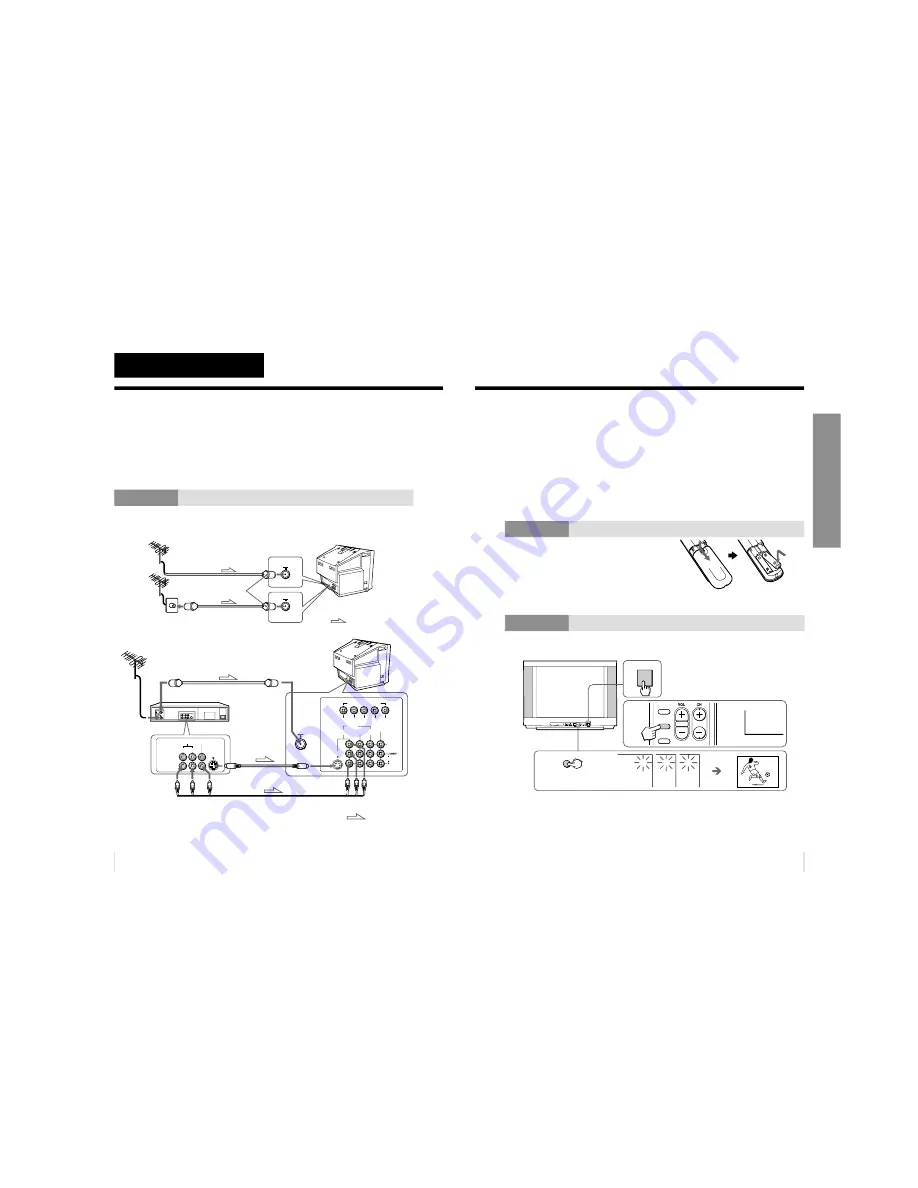
Step 1

Connect the antenna

If you wish to connect a VCR, see the 

Connecting a VCR

 diagram below.

Connecting a VCR

To watch the video input, press VIDEO (see page 12).

Tip

• With the “VIDEO MULTI SYSTEM” input terminal, you can also receive

PAL, NTSC and SECAM video signals when using the VIDEO IN 1, 2 or 3
jacks, or the VIDEO 3 INPUT jacks at the front of your TV.

: Signal flow

or

Antenna cable (not supplied)

Antenna cable (not supplied)

Rear of TV

F connector
(not supplied)

To video and
audio outputs

To
S video output

Audio/Video cable
(not supplied)

: Signal flow

To


S VIDEO

input

VCR

Antenna cable (not supplied)

To antenna
output

Rear of TV

VIDEO (yellow)
AUDIO-L (MONO) (white)
AUDIO-R (red)

To VIDEO IN
1, 2, or 3

S video cable
(not supplied)

VIDEO

VIDEO IN

VIDEO OUT

AUDIO

R       L

1

2

3

R

L

Y

C

B

C

R

COMPONENT VIDEO(DVD) IN

AUDIO

VIDEO

VIDEO

IN

MONITOR

OUT

S VIDEO

To 

8

(antenna)

5

Using Your New TV

Using Y

our New TV

Notes

• If you connect a monaural AUDIO VCR, connect the yellow plug to

VIDEO (the yellow jack) and the black plug to AUDIO-L (MONO)
(the white jack).

• If you connect  a VCR  to the 

8

 (antenna) terminal, preset the signal

output from the VCR to the program number 0 on the TV.

• When both the S VIDEO and VIDEO IN 1 input are connected, the

S VIDEO input is automatically selected.  To view the video input to
VIDEO IN 1, disconnect the S video cable.

• Do not connect video equipment to the VIDEO 3 INPUT jacks at the front

and VIDEO IN 3 (video input) jack at the rear of your TV at the same time;
otherwise the picture will not be displayed properly on the screen.

• When no signal is input from the connected video equipment, the TV

screen becomes blue.

 Step 2

Insert the batteries into
the remote

Note

• Do not use old batteries or different types of batteries together.

 Step 3

Preset the channels automatically

Tips

• To stop the automatic channel presetting, press MENU.
• If your TV has preset an unwanted channel or cannot preset a particular

channel, then preset your TV manually (see page 10).

• The AUTO PROGRAM button on the remote works as the AUTO PROGR

button on the TV.

1

1

2

3

2

3

SLEEP

CABLE

AUTO 

PROGRAM

AUTO PROGRAM

    AUTO
   PROGR

CABLE: ON

3

1

POWER

Front panel

Summary of Contents for TRINITRON KV-XA25N90

Page 1: ...ppines SCC U51B A TRINITRON COLOR TV SERVICE MANUAL BG 3R RM 914 RM 954 CHASSIS MODEL COMMANDER DEST CHASSIS NO RETURN MENU PIC MODE WAKE UP SOUND MODE SLEEP CABLE AUTO PROGRAM ADD ERASE FAVORITE SURROUND MTS MUTING DISPLAY POWER VIDEO TV 1 2 5 8 7 4 0 3 9 6 1 4 7 2 5 8 0 3 6 9 FAVORITE SOUND MODE PIC MODE ENTER MENU A B SURROUND ...

Page 2: ...00 mVrms Three input lines available S Video Input 2 Y 1 Vp p 75 ohms unbalanced sync negative C 0 286 Vp p 75 ohms Component Video Input 1 Phono jacks Y 1 Vp p 75 ohms sync negative CB 0 7 Vp p 75 ohms CR 0 7 Vp p 75 ohms Audio 500 mVrms 2 Headphone Output 1 Stereo minijack Picture tube 25 inch Tube size cm 64 Measured diagonally Screen size cm 60 Measured diagonally Dimension w h d mm 696 539 50...

Page 3: ...Input 2 Y 1 Vp p 75 ohms unbalanced sync negative C 0 286 Vp p 75 ohms COMPONENT VIDEO Output 1 Stereo minijack DVD IN Picture tube 25 inch Tube size cm 64 Measured diagonally Screen size cm 60 Measured diagonally Dimension w h d mm 696 513 499 Mass kg 38 Design and specifications are subject to change without notice SAFETY RELATED COMPONENT WARNING COMPONENTS IDENTIFIED BY SHADING AND MARK ON THE...

Page 4: ... Adjustment 47 4 4 G2 SCREEN and White Balance Adjustment 48 5 CIRCUIT ADJUSTMENTS 5 1 Adjustment With Commander 49 5 2 Adjustment Method 49 5 3 Picture Quality Adjustments 55 5 4 Deflection Adjustment 55 5 5 H Trapezoid Adjustment 56 5 6 A Board Adjustment After IC003 Replacement 56 5 7 Picture Distortion Adjustment 57 6 DIAGRAMS 6 1 BLOCK DIAGRAM 59 6 2 CIRCUIT BOARDS LOCATION 61 6 3 SCHEMATIC D...

Page 5: ... come on No power is supplied to the TV AC power supply is faulty Power does not come on Load on power line is shorted Has entered standby state after horizontal raster Vertical deflection pulse is stopped Power line is shorted or power supply is stopped No raster is generated CRT cathode current detection reference pulse output is small Power is shut down shortly after this return back to normal ...

Page 6: ... the screen To Bring Up Screen Test In standby mode press buttons on the remote commander sequentially in rapid succession as shown below Screen display channel 5 Sound volume Power ON Note that this differs from entering the service mode mode volume Self Diagnosis screen display STANDBY SLEEP lamp Lamp ON 0 3 sec Lamp OFF 3 sec Lamp OFF 0 3 sec 2 times 3 times Diagnostic Item Flash Count B overcu...

Page 7: ...unit 6 SELF DIAGNOSTIC CIRCUIT B overcurrent ªOCPº Occurs when an overcurrent on the B 135 line is detected by Q604 If Q604 go to ON and the voltage to pin 18 of IC301 should go down when V SYNC is more than seven verticals in a period the unit will automatically turn off Vertical deflection stopped Occurs when an absence of the vertical deflection pulse is detected by Q509 and IC001 shut down the...

Page 8: ...use only Do not use the TV in any vehicle or where it may be subject to excessive dust heat moisture or vibrations Do not block the ventilation openings of the TV Do not install the TV in a confined space such as a bookcase or built in cabinet For children s safety do not leave children alone with the TV Do not allow children to climb onto it Do not plug in too many appliances to the same power so...

Page 9: ...h water 5 Using Your New TV Using Your New TV Notes If you connect a monaural VCR connect the yellow plug to the yellow jack and the black plug to L MONO the white jack If you connect a VCR to the antenna terminal preset the signal output from the VCR to the program number 0 on the TV If both S video input and t 1 video input at the rear of your TV are input at the same time the S video input is a...

Page 10: ...i disc player DVD camcorder video game or stereo system To watch the video input of the connected equipment press t see page 11 Connecting a camcorder video game equipment using the t video input jacks Notes You can also connect video equipment to the t 1 2 or 3 video input jacks at the rear of your TV If both S video input and t 3 video input at the front of your TV are input at the same time the...

Page 11: ... Y CB and CR under component video input on your TV to the COMPONENT VIDEO OUT Y CB and CR output connectors on your DVD player Since the high quality pictures on a DVD disc contain a lot of information picture noise may appear In this case adjust the sharpness SHARP in the ADJUST menu of the PICTURE MODE menu see page 19 Connect your DVD player directly to your TV Connecting the DVD player throug...

Page 12: ...emporarily Turn off completely Adjust the volume Mute the sound Watch the video input VCR camcorder etc Jump back to the previous program number Display the on screen information Press 1 The 1 indicator on the TV lights up red on the TV 2 t to select VIDEO 1 VIDEO 2 VIDEO 3 or DVD To return to the TV program press a or t on the TV JUMP The picture sound and either the program number or video input...

Page 13: ...FF SLEEP TIMER 90M After 30 minutes No Sleep Timer After 60 minutes After 90 minutes Watching the TV continued 13 Advanced Operations Advanced Operations SOUND MODE Selecting the picture and sound modes You can select picture and sound modes and adjust the setting to your preference in PERSONAL option Selecting the picture mode Press PIC MODE repeatedly until you get the desired picture mode Selec...

Page 14: ... The surround feature enables you to enjoy the sound effects of a concert hall or movie theater Select To TruSurround listen to the surround sound that spreads out to the rear of a room OFF turn off the surround sound Tip You can also select the surround option using the menu see Changing the SOUND setting on page 20 The surround of your TV is categorized as TruSurround TM is a trademark of SRS La...

Page 15: ...ls automatically MANUAL PROGRAM Preset channels manually TV SYS Change the TV system B G t I t D K t M The BBE is manufactured by Sony Corporation under license from BBE Sound Inc It is covered by U S Patent No 4 638 258 and No 4 482 866 The word BBE and the BBE symbol are the trademarks of BBE Sound Inc Guide mark icon 17 Adjusting Your Setup MENU How to use the menu You can use the buttons on th...

Page 16: ...mode is selected you can receive the last adjusted picture settings from the ADJUST option see page 19 Note For details on the options under PICTURE MODE see page 13 To return to the normal screen Press MENU ENTER ENTER MENU FAVORITE SOUND MODE PIC MODE ENTER MENU A B SURROUND 19 Adjusting Your Setup MENU ENTER COLOR 80 Adjusting the ADJUST items under PICTURE MODE 1 Press or to select the desired...

Page 17: ...ress MENU ENTER ENTER SOUND MODE SOUND I NTE L L I GENT VOL OF F SURROUND OF F F DYNAM I C PER SOUND SONA L I NTE L L I GEN SOF T S S URROUND O OUND MODE DRAMA AD J UST C DYNAM I ENTER MENU FAVORITE SOUND MODE PIC MODE ENTER MENU A B SURROUND 21 Adjusting Your Setup MENU BALANCE 00 ENTER Adjusting the ADJUST items under SOUND MODE 1 Press or to select the desired item e g BALANCE then press ENTER ...

Page 18: ...al screen Press MENU 23 Adjusting Your Setup MENU Adjusting each program number settings PROGRAM SETUP 1 Select PROGRAM SETUP from the SETUP menu 2 Select PR and press ENTER Press or to select the desired program number you want to adjust then press ENTER 3 Press or to select the desired item e g CHILD LOCK then press ENTER Select To PR select the desired program number SKIP skip unwanted or unuse...

Page 19: ... to select either B G I D K or M then press ENTER 25 Adjusting Your Setup MENU Presetting channels manually 1 After selecting MANUAL PROGRAM select the program number to which you want to preset a channel 1 Make sure PR is selected then press ENTER 2 Press or until the program number you want to preset e g program number 10 appears on the menu then press ENTER 2 Select the desired channel 1 Make s...

Page 20: ...am number will be unlocked automatically see page 23 The TV system TV SYS and the fine tuning FINE settings are memorized for each program number Changing the Channel Preset CH PRESET setting continued 27 Additional Information Additional Information Self diagnosis function Your TV is equipped with a self diagnosis function If there is a problem with your TV the 1 indicator flashes red The number ...

Page 21: ... sound Distorted picture Noisy sound Good picture Noisy sound No picture No sound Page 4 25 24 24 4 10 10 29 Additional Information Press 2 to increase the volume level Press to cancel the muting Do not use a hair dryer or other equipment near the TV Adjust the antenna direction for minimum interference Contact a Sony dealer for advice Use a highly directional antenna Use the fine tuning FINE func...

Page 22: ...alfunction The TV s demagnetizing function is working This does not indicate a malfunction Keep external speakers or other electrical equipment away from the TV Display the SETUP menu and adjust PIC ROTATION so that the picture is aligned to the TV screen Use the fine tuning FINE function Contact your nearest Sony service center Page Troubleshooting continued 31 Additional Information Overview of ...

Page 23: ...e Menu operations MENU or ENTER Turn off temporarily or turn on the TV 10 Select program number 10 Input numbers 10 Adjust volume 11 Select TV or video input 11 Display the TV program 11 Mute the sound 11 Display on screen information 11 Jump to previous program number 11 Set TV to turn on automatically 12 Set TV to turn off automatically 12 Select picture mode 13 Select sound mode 13 Display favo...

Page 24: ...only Do not use the TV in any vehicle or where it may be subject to excessive dust heat moisture or vibrations Do not block the ventilation openings of the TV Do not install the TV in a confined space such as a bookcase or built in cabinet For children s safety do not leave children alone with the TV Do not allow children to climb onto it Do not plug in too many appliances to the same power socket...

Page 25: ...ble not supplied VIDEO VIDEO IN VIDEO OUT AUDIO R L 1 2 3 R L Y CB CR COMPONENT VIDEO DVD IN AUDIO VIDEO VIDEO IN MONITOR OUT S VIDEO To 8 antenna 5 Using Your New TV Using Your New TV Notes If you connect a monaural AUDIO VCR connect the yellow plug to VIDEO the yellow jack and the black plug to AUDIO L MONO the white jack If you connect a VCR to the 8 antenna terminal preset the signal output fr...

Page 26: ...ee page 12 1 2 3 R L Y CB CR COMPONENT VIDEO DVD IN AUDIO VIDEO VIDEO IN MONITOR OUT S VIDEO VIDEO yellow AUDIO L MONO white AUDIO R red Rear of TV To 8 antenna To video and audio inputs Audio system To audio inputs VCR Signal flow To MONITOR OUT Antenna cable not supplied Audio Video cable not supplied or To antenna output or Signal flow Video game equipment Camcorder To video and audio outputs T...

Page 27: ...s may be labeled differently When connecting to the COMPONENT VIDEO DVD IN jacks on your TV you must connect Y CB and CR to receive the video signals and connect L and R to receive analog audio signals To component video output Component video cable not supplied DVD player To audio output Audio cable not supplied Signal flow To COMPONENT VIDEO DVD IN Rear of TV VIDEO R AUDIO L LINE OUT Y COMPONENT...

Page 28: ...LEEP CABLE AUTO PROGRAM ADD ERASE FAVORITE SURROUND 1 2 5 8 7 4 0 3 9 6 11 Using Your New TV Using Your New TV Watching the TV This section explains various functions and operations available while watching the TV Most operations can be done using the remote 1 Press POWER to turn on the TV When the TV is in standby mode the STANDBY indicator on the TV is lit red press POWER on the remote or CHANNE...

Page 29: ...F WI DE MODE OF F DE DYNAM I E COLOR SYS AUTO SETUP PROGRAM SETUP P I C ROTAT I ON NGL I SH L ANGUAGE L ANGUAGE COLOR SYS SETUP PROGRAM SE P I C ROTAT I ENGL I SH Watching the TV continued 13 Using Your New TV Using Your New TV Setting the Wake Up timer 1 Press WAKE UP until the desired period of time appears The Wake Up timer starts immediately after you have set it 2 Select the channel number or...

Page 30: ... menu see Changing the PICTURE setting on page 20 and Changing the SOUND setting on page 22 Selecting the picture and sound modes You can select picture and sound modes and adjust the setting to your preference in the PERSONAL option PIC MODE SOUND MODE PERSONAL DYNAMIC SOFT STANDARD PIC MODE SOUND MODE DYNAMIC PERSONAL SOFT DRAMA RETURN MENU PIC MODE WAKE UP SOUND MODE SLEEP CABLE AUTO PROGRAM AD...

Page 31: ...onal issued and pending foreign patents SURROUND RETURN MENU PIC MODE WAKE UP SOUND MODE SLEEP CABLE AUTO PROGRAM ADD ERASE FAVORITE SURROUND SURROUND TruSurround SURROUND OFF SURROUND 17 Advanced Operations Advanced Operations Enjoying stereo or bilingual programs You can enjoy stereo sound or bilingual programs of MTS stereo system When receiving a MTS program press MTS repeatedly until you rece...

Page 32: ...4 638 258 and No 4 482 866 The word BBE and the BBE symbol are the trademarks of BBE Sound Inc Return icon CH PRESET icon SETUP icon SOUND icon Name of the current menu PICTURE icon Menu level 3 Menu level 2 Guide mark icon Menu level 1 L ANGUAGE SETUP COLOR Y S S P I C ROTAT I ENGL I SH CHANNE L SE 19 Adjusting Your Setup MENU Adjusting Your Setup MENU How to use the menu You can use the buttons ...

Page 33: ...mode 16 9 picture signal Press or to select ON then press RETURN To cancel select OFF then press RETURN optimize picture quality Press or to select ON then press RETURN To cancel select OFF then press RETURN P I CTURE MODE I NTE L L I GENT P I CTURE WI DE D MO E DYNAM I C TANDARD SOF T PERSON AD J UST AL S 21 Adjusting Your Setup MENU Adjusting Your Setup MENU Adjusting the ADJUST items under PICT...

Page 34: ...E WAKE UP SOUND MODE SLEEP CABLE AUTO PROGRAM ADD FAVORITE SURROUND RETURN SOUND MODE SOUND I NTE L L I GENT VOL OF F SURROUND OF F DYNAM I C RETURN SOUND MODE PE SOUND RSONA L I NTE L L I GENT SOF T DRAMA SURROUND OF AD J UST DYNAM I C MENU RETURN 23 Adjusting Your Setup MENU Adjusting Your Setup MENU Adjusting the ADJUST items under SOUND MODE 1 Press or to select the desired item e g BALANCE th...

Page 35: ...usting Your Setup MENU Adjusting each channel number settings CHANNEL SETUP 1 Select CHANNEL SETUP from the SETUP menu 2 Select CH and press RETURN Press or to select the desired channel number you want to adjust then press RETURN 3 Press or to select the desired item e g ADD ERASE then press RETURN Select To CH select the desired channel number ADD ERASE preset the selected channel manually Press...

Page 36: ...ve only VHF and UHF broadcast channels select OFF then press RETURN MENU RETURN RETURN CH PRESET CAB L E ON AUTO PROGRAM RETURN R CH PRESET CAB L OF F A ON AUT E O PROG RETURN MENU PIC MODE WAKE UP SOUND MODE FAVORITE SURROUND 1 2 5 8 7 4 0 3 9 6 27 Additional Information Additional Information Additional Information Self diagnosis function Your TV is equipped with a self diagnosis function If the...

Page 37: ...volume level is too low The sound is muted Broadcast signal has a transmission problem There is local interference from cars neon signs hair dryers power generators etc Broadcast signals are reflected by nearby mountains or buildings The antenna direction is inappropriate Use of a booster is inappropriate The color level setting is too low The color system setting is inappropriate for video input ...

Page 38: ...ck the antenna cable and connection on the TV VCR and on the wall Adjust the antenna direction Contact a Sony dealer for advice Press MTS until a better sound is heard Keep external speakers or other electrical equipment away from the TV Display the SETUP menu and adjust PIC ROTATION until the picture is optimal Contact your nearest Sony service center Page Good morning 31 Additional Information A...

Page 39: ...vorite Channel operations FAVORITE 1 6 SURROUND Stereo bilingual operations MTS Menu operations MENU RETURN Preset channels automatically Receive cable TV programs Preset channels manually Input numbers Confirm input number Turn off temporarily or turn on the TV Select channel number Adjust volume Select TV or video input Display the TV program Mute the sound Display on screen information Jump to ...

Page 40: ...screws washer head P 4 16 2 Two screws BVTP 3 12 3 F Board bracket 5 Two claws 1 Three connectors 4 F board 2 Three screws BVTP 4 16 1 Eight screws BVTP 4 16 3 Rear Cover 2 1 3D SPEAKER BOX REMOVAL 1 3D Speaker box assy KV XA25M83 ONLY Black wire Red wire Note 1 Disconnect the speaker connection on the right side 2 Undress necessary wires that creates tension while placing the chassis into Service...

Page 41: ...RDS REMOVAL One screw BVTP 4x16 6 Terminal bracket J Board KV XA25M83 J1 Board Except KV XA25M83 Four screws BVTP 3 12 4 5 2 9 TERMINAL BRACKET REMOVAL One screw BVTP 4x16 6 Two claws 5 Terminal bracket 1 J Board KV XA25M83 J1 Board Except KV XA25M83 4 Two screws BVTP 3 12 2 Four screws BVTP 3 12 3 2 10 B1 BOARD REMOVAL 2 One Connector 1 B1 Board 2 11 H BOARD REMOVAL 2 Two connectors 3 Two connect...

Page 42: ...jects 2 Do not press the rubber too hard so as not to damage the inside of anode cap A metal fitting called the shatter hook terminal is built into the rubber 3 Do not turn the foot of rubber over too hard The shatter hook terminal will stick out or damage the rubber a a b b c Anode Button 2 13 PICTURE TUBE REMOVAL Note Please remove necessary CRT support located on top left top right prior to rem...

Page 43: ...y will be displayed for 10 sec after IK status gets stable As a result some items will be reset to an initial condition shipment condition wheareas some other remains at the last selection by user Items that remains at the last selection by user Reset Items Program No Favourite CH Setup PIC rotation OSD Language Fine tuning TV System Skip only when in RF mode 1 Not used for these models Video inpu...

Page 44: ...he pattern generator Contrast Brightness 2 Position neck assy as shown in Fig4 1 3 Set the pattern generator raster signal to a green raster 4 Move the deflection yoke to the rear and adjust with the purity control so that the green is at the center and the blue and the red take up equally sized areas on each side See Figures 4 2 through 4 4 5 Move the deflection yoke forward and adjust so that th...

Page 45: ...p of each other at the center of the screen 2 Moving vertically adjust the V STAT magnet so that the red green and blue dots are on top of each other at the center of the screen 3 If the H STAT variable resistor cannot bring the red green and blue dots together at the center of the screen adjust the horizontal convergence with the H STAT variable resistor and the V STAT magnet in the manner given ...

Page 46: ...is adjustment adjust the horizontal static convergence and the vertical static convergence 5 Y separation axis correction magnet adjustment 1 Receive the cross hatch signal and adjust PICTURE to MIN and BRIGHTNESS to STANDARD 2 Adjust the Y separation axis correction magnet on the neck assembly so that the horizontal lines at the top and bottom of the screen are straight Blue Red VM1 board Blue Re...

Page 47: ... b Adjust focus VR so that the lion teeth becomes just focus 25 only 4 Change the receiving signal to white pattern and blue back 5 Confirm magenta ring is not noticable Incase magenta ring is obvious adjust FOCUS VR to balance between MAGENTA RING and FOCUS TLV Rotate TLV 2 VOL 29 34 on DY Rotate TLV VOL 25 on DY XCV Rotate XCV Adj core on DY YCH Rotate YCH VOL on DY TLH Insert TLH Correction Pla...

Page 48: ...SUB BRIGHT ADJUSTMENT 1 Set to service mode 2 Input a staircase signal of black to white from the pattern generator 3 BRIGHTNESS 50 PICTURE MINIMUM 4 Select SBR WHB7 with 1 and 4 and adjust SBR WHB7 level with 3 and 6 so that the second stripe from the right is dimly lit 4 4 G2 SCREEN AND WHITE BALANCE ADJUSTMENT 1 G2 SCREEN ADJUSTMENT 1 Set the PICTURE to normal 2 Put to VIDEO input mode without ...

Page 49: ...0Hz or vice versa 2 Write 50Hz adjustment data to 60Hz or vice versa n DISPLAY n 5 n VOL n POWER 5 2 ADJUSTMENT METHOD Item Number 00 of device GEO This explanation uses H Position as an example 1 Select GEO 00 HPS with the 1 and 4 buttons 2 Raise lower the data with the 3 and 6 buttons 3 Select the optimum state The standard is 1F for PAL reception 4 Write with the MUTING button The display chang...

Page 50: ...h t o C I M A N Y D 2 7 D 0 0 A C B 2 C 2 7 F 1 3 0 T C R F 0 f f o t u C R s r e h t o M A C E S 0 3 9 0 0 A D B 3 C 0 3 7 4 0 T C G F 0 f f o t u C G s r e h t o M A C E S 4 7 A 0 0 A E B 4 C 4 7 7 5 0 T C B F 0 f f o t u C B s r e h t o M A C E S 0 3 A 0 0 A E B 4 C 0 3 7 6 0 N M B F 1 a t a D m u m i n i M s s e n t h g i r B 2 7 8 0 0 A 2 2 2 6 5 1 7 0 R B S F 3 l o r t n o C s s e n t h g i ...

Page 51: ...d i v 4 5 F 0 0 A B 2 4 5 1 7 1 N O R 1 N O R d e z i r o m e m t o n 2 1 0 0 A 1 8 2 1 8 1 N O G 1 N O G d e z i r o m e m t o n 1 1 0 0 A 1 8 1 1 9 1 N O B 1 N O B d e z i r o m e m t o n 0 1 0 0 A 1 8 0 1 A 1 N O P 1 N O P d e z i r o m e m t o n 7 0 0 0 A 0 8 7 1 B 1 N X A 1 W S S I X A s r e h t o C S T N C I M A N Y D r o f y l n o 0 7 0 0 A B 3 C 3 6 2 7 3 0 1 C 1 L S R 1 L E S B G R 0 C 0 ...

Page 52: ... 6 0 7 D 6 P V S 0 0 F B S F 3 0 f L L E B M A C E S 2 7 C 1 H A 8 S 9 3 1 2 A X C 4 A 1 1 2 7 2 2 1 0 S O H F 0 n o i t a l l i c s O H 4 7 C 0 4 A C 0 4 7 7 2 0 U H S F 0 l o r t n o C e u H b u S o e d i V V T 2 7 5 0 4 A F 2 D 2 2 5 8 3 0 C F A 3 n i a G C F A o e d i V V T 0 F 0 4 A 2 3 1 3 0 1 1 P I P 0 0 L D S F 0 T C E L E S t u p t u O f o y a l e D 3 6 1 0 H 6 D X 8 8 2 9 A D S 4 A C 1 3...

Page 53: ... 0 6 7 9 0 0 5 7 P X C 0 A F 4 0 0 5 0 M F A 1 h c t i w S M F o t u A 0 A F 4 1 1 6 0 B F R 3 l o r t n o C F P B C 0 A 0 5 4 5 0 7 0 O V T 7 t e s f f O e l g n A V o t t l i T 0 A 0 5 0 2 2 8 0 L B D 1 n o i t c n u F k c a b e u l B e l b a s i D 0 A F 4 2 0 9 0 O S S 3 x 8 3 X 6 2 X 4 1 f f O 0 n o i t p O h c r a e S d e e p S 0 A F 4 6 7 1 A 0 H C S F 7 n o i t i d n o C g n i p p i h S r o...

Page 54: ...is set to 3 AV Input Dis Fav Disable Favorite Channel Effective For XF L 21 14 Models Only 1 1 1 1 1 1 DVD Input 1 1 1 Dis Fav 0 0 0 Thai Bil 0 0 0 HDEV 0 0 0 NICAM 0 0 0 TOP 0 0 0 AV Input No OPB1 OP2 PIC Rotate 1 PIC Rotation Switch 0 disabled 1 enabled 2199 Curve 1 2199 volume Curve Selection 0 Others 1 2199 Volume Curve Auto PIC 3 Auto Picture Improvement 0 off PNC1 PNC2 1 activate PNC1 PNC2 A...

Page 55: ...commander to write the data 7 Adjust SAJ 1 SHU as step 3 to 6 when receiving TV mode 5 4 DEFLECTION ADJUSTMENT NORMAL MODE 50Hz 1 Set to Service Mode 2 Using the 1 and 4 button select category GEO Service Mode 3 Raise lower the data using the 3 and 6 buttons Select and adjust the following items to obtain optimum image Service Item GEO 00 HPS H POSITION 01 HSZ H SIZE 02 PAP PIN AMP 03 TLT TILT 04 ...

Page 56: ... following items to obtain optimum image Service Item GEO 00 HPS H POSITION 02 PAP PIN AMP 03 TLT TILT 04 VPS V POSITION 08 BOW AFC BOW 09 AGL AFC ANGLE 0A UPN UPPER CORNER PIN 0B LPN LOWER CORNER PIN 19 After confirm WIDE MODE ON OFF Note For Deflection Adjustment set PICTURE MODE to SOFT 5 5 H TRAPEZOID ADJUSTMENT 1 Receive cross hatch dot signal 2 Adjust RV1801 on C6 board to make H Trapezoid d...

Page 57: ...SZ H SIZE GEO 3 TLT TRAPEZIUM GEO 0A UPN UPPER CORNER PIN GEO 0B LPN LOWER CORNER PIN GEO 5 VSZ V SIZE GEO 0 HPS H POSITION GEO 9 AGL AFC ANGLE GEO 8 BOW AFC BOW GEO 2 PAP PIN AMP GEO 4 VPS V POSITION GEO 7 VLN V LINEARITY GEO 6 SCO VERTICAL S Correction PICTURE DISTORTION ADJUSTMENT 2 H TRAPEZOID DAC 4 HTR ...

Page 58: ... 58 KV XA25M80 XA25M83 XA25N90 RM 954 RM 914 MEMO ...

Page 59: ...7 4 2 43 1 2 4 3 6 45 COMBY In COMB C In CV Y in C in CV Y out V1 V In V1 L In V1 R In V1 Y In V1 C In 7 8 10 V2 V In V2 L In V2 R In 14 16 15 17 11 18 29 28 26 18 CN1304 V3 L In V3 R In V3 CV Y In V3 C In V out2 L out2 R out2 Y Y Y U V U V U V B G R BLK H HALF 28 29 30 34 33 32 41 40 39 31 16 15 13 20 21 H DRIVE H PULSE E W VD PIN CONT IC502 NJM2903M HLT T504 PMT T505 H OUT Q511 2SC4927 HDT T501 ...

Page 60: ...underline PAL SECAM NTSC 3 58 NTSC 4 43 Readings are taken with a 10M digital m ultimeter Voltage are dc with respect to ground unless otherwise noted Voltage variations may be noted due to normal produc tion tolerances All voltage are in V Cannot be measured Circled numbers are waveform references B bus B bus signal path Reference information RESISTOR RN METAL FILM RC SOLID FPRD NONFLAMMABLE CARB...

Page 61: ...901 47 10k 330 10k 330 75 220 220 75 330 330 1k 1 8k 3 3k 5 6k 470 0 01 1 DTC144ESA LED DRIVE DTC144ESA LED DRIVE SPB 25MVWF WAKE UP INDICATOR 100 100 0 01 MPS 10k 10k 4P VH 2 2k 3P AC PUSH SW NNCD9 1A T1 PROTECTOR NNCD9 1A T1 PROTECTOR NNCD9 1A T1 PROTECTOR NNCD9 1A T1 PROTECT NNCD9 1A T1 PROTECT 47 25V 4P BLK S MICRO 6P WHT S MICRO EL0606 EL0606 47 47 4P VH 7 5M M 4 7 4 7 470p B JW 5MM JW 5MM 7 ...

Page 62: ...0k CHIP 0 0 1 B CHI P 2SA1162 G 2SA1162 G VCC FALL DETECTOR 0 CHIP 1k CHIP 10P BTOB 220 16V 1 0 k CHI P 10k CHIP 2SC2712 YG BUFFER 100p CH CHIP 1 0 0 p CH CHI P 2SC2712 YG BUFFER 0 CH I P 0 CH I P NS ROT 7 V 5 V JOINT A1 JOINT A2 JOINT A3 JOINT A4 JOINT A5 JOINT A6 JOINT A7 JOINT A8 JOINT A9 JOINT A10 JOINT A11 JOINT A12 JOINT A13 JOINT A14 JOINT A15 JOINT A16 JOINT A17 JOINT A18 JOINT A19 JOINT A...

Page 63: ...16V 47 25V 47 47 16V 100 10V 10k CHIP 100 CHIP 10P BTOB MSP RESET 0 CHIP 680 CHIP 18k CHIP 0 CHIP 1 5k CHIP 0 CHIP CXA2159S Y C JUNGLE 9V 30V JOINT A1 JOINT A2 JOINT A3 JOINT A4 JOINT A5 JOINT A6 JOINT A7 JOINT A8 JOINT A9 JOINT A10 JOINT A11 JOINT A12 JOINT A13 JOINT A14 JOINT A15 JOINT A16 J O I N T 5 6 J O I N T 5 7 J O I N T 5 8 J O I N T 5 9 J O I N T 6 0 J O I N T 6 1 J O I N T 6 2 J O I N T...

Page 64: ...1 2 Y G I N V E R T E R 4 7k CHIP 470 CHIP 100p CH CHIP 100p CH CHIP 100p CH CHIP UN2213 SWITCH 2 S C 2 7 1 2 Y G 56k CHIP 27k CHIP 330 CHIP 2SC2712 YG AMPLIFIER 390 CHIP 470 CHIP 27k CHIP 56k CHIP 2SC2712 YG AMPLIFIER 470 CHIP 330 CHIP 390 CHIP 10M CHIP 4 7k CHIP 0 1 25V B CHIP DTA114TK SYSTEM CONTROLLER ST BY 5 V S T B Y N S M U T E A B L 7V 1 1 V B S T B Y 7 V J O I N T 1 J O I N T 2 J O I N T ...

Page 65: ... A43 JOINT A44 JOINT A45 JOINT A46 JOINT A47 JOINT A48 JOINT A49 JOINT A50 JOINT A51 JOINT A52 JOINT A53 JOINT A54 JOINT A55 JOINT A56 JOINT A57 JOINT A58 JOINT A59 J O I N T 5 6 J O I N T 5 7 J O I N T 5 8 J O I N T 5 9 J O I N T 6 0 J O I N T 6 1 J O I N T 6 2 J O I N T 6 3 J O I N T 6 4 J O I N T 6 5 J O I N T 6 6 J O I N T 6 7 J O I N T 6 8 J O I N T 6 9 J O I N T 7 0 J O I N T 7 1 J O I N T 7...

Page 66: ...25V 22 1 1UH JW 5 MA111 TX PROTECT D T Z T T 1 1 1 5 B C L A MP 0 047 B CHIP 1k CHIP 10k CHIP DTZ10B CLAMP 2200p 500V E 1 803 586 11 ERC04 06SE SNUBBER ERC04 06SE SNUBBER RD30ESB2 2 S K 2 8 4 5 L B 1 0 2 S WI T C HI N G 680 CHIP 2SC2712 YG SWITCHING 2 2k CHIP 22M 1 2W 470k RN RD6 8ES B1 PROTECT 470 CHIP D1N20R PROTECT MA111 TX SENSING 10k CHIP MA111 TX SENSING 47k CHIP D1NS4 470p 250V B STB LHL08 ...

Page 67: ...ONTROL MA111 TX 0 0033 B CHIP 220 16V ELIZ PIN OUT 0 0056 100V 680p 2kV B 680p 2kV B ERC06 15S DAMPER ERC06 15S DAMPER RU4AM T4 PIN DAMPER 1000PF 7 5MM COIL 2SC2688 LK H DRIVE 1K 3W RS 0 047 200V PT 1000P 500V 820p 500V B 5 6k 1W RS 0 001 33 160V 1 1UH 0 0033 630V 1 1UH 47 JW 5 1k 56k 470K 3 3k 10k CHIP 330 6 8K 2 2 0 2 2 k CHI P 6 8k CHIP 2 2K 10K CHIP 10K 4700p B CHIP 15 0MM PMT 100 22K 100 3W R...

Page 68: ... 470 1 2W FPRD MA111 TX 10 REGULATOR CONTROL 680p 1 5kV PP 470p 250V B 470p 250V B 15k 3W RS 470p CH CHIP AK04V0 0 22 2W RS 0 22 2W RS 10EL32N TBS 10ELS2N TB2 82k 3W RS 82k 3W RS 0 022 400V 100p 1kV SL RU 1P 10ELS2N TB2 100 25V 680p 500V B 560 160V 2200 2200 16V 4 7k 1W RS 0 1 200V PT SE 135N 220 16V 100 10V 1 755 299 11 1SS119 25 DAMPER 2SC2785 HFE RELAY DRIVE 1SS119 25 PROTECT 470p B 0UH 2P MINI...

Page 69: ... 220p 500V B 0 47 1 2W FPRD 470 25V TDA8172 V OUT 0 01 1 5 FPRD 33K 10k RN CP 4 7k RN 8 2K 68k RN 10k RN 8 2k RN 470 25V 15k CHIP 10k 3 3k 4 7k CHIP JW 5 JW 5 33k CHIP LHL08 0 1 F CHIP 0 1 MPS 5 6k CHIP 1SS355TE 17 DETECT 1SS355TE 17 PROTECT 4 7k CHIP 15k CHIP 220 RN CP 100 16V 1SS355TE 17 DETECT 1SS355TE 17 DETECT 1SS355TE 17 DETECT 470p 500V B 1P 0 CHIP 0 CHIP 2 2 5P S MICRO 1SS119 25 2SC2712 YG...

Page 70: ...0 CHI P 10 0 CHI P 10 0 1 25 V F CHI P 10 0 CHI P 100 CHI P 100 25V 470p CH CHIP 470p CH CHIP 1 16V F CHIP 0 022 B CHIP 0 022 B CHIP 0 022 B CHIP 0 022 B CHIP 0 1 25V F CHIP 10 10 25V BP 10 25V BP 0 CHIP 2 2 16V F CHIP 0 CHIP FLR50 220k CHIP 220k CHIP 10 0 CHI P JW 5MM 10k CHIP 10k CHIP 22k CHIP 22k CHIP 0 CHIP 100 CHIP 1 00 CHI P 1 00 CHI P 10 0 CHI P 100 CHI P 1 00 CHI P 100 CHIP 47 16V 33 25V 4...

Page 71: ... 0 001 B 470p B 470p B 470p B 560p B 330p B 100 16V 4 7 250V 1000 25V 1P TAB 1P TAB 6P WHT S MICRO 1P TAB 4P WHT S MICRO 3P WHT S MICRO 1SS119 25 PROTECT 1SS119 25 PROTECT 1SS119 25 PROTECT 1SS119 25 PROTECT 1SS119 25 PROTECT 1SS119 25 PROTECT 1SS119 25 PROTECT 1SS119 25 PROTECT 1SS119 25 PROTECT 1SS119 25 PROTECT 1SS1 19 25 PROTECT 1 SS1 19 25 PROTECT 1SS119 25 PROTECT HZS9 1NB2 PROTECT 1SS119 25...

Page 72: ...19 R5901 R5927 C5920 D5901 C5918 Q5907 C5921 L5902 JW5900 R5925 CN5904 CN2801 330 560 820 330 16V 33 160V 2 2 160V 0 047 200V PT 0 1 200V PT 470 10V 470 10V 100 16V 100 16V 0 001 PT 0 001 PT 0 047 PT 0 047 PT 0 0047 500V E 10 2W RS 68 68 120 120 220 1k 1k 1k 1 5k 10k 10k 47k 68k 68k 1 5 FPRD 1 5 FPRD 560 FPRD 1k FPRD 10 0MM 5MM 7P S MICRO 1SS119 25 1SS119 25 RD39ES B2 DC BIAS RD39ES B2 DC BIAS 2SA...

Page 73: ...30p B 47 47 330p B 220 47 220k 220k 100 100 1 1 75 8P 5P TERMINAL PUSH GND GND DVD Y DVD BY DVD RY GND DVD L DVD R Y B Y R Y L R R L DVD TERMINAL B SSSBG3R J1 XA25M80 TO B1 BOARD CN1501 GND GND D2415 HZS9 1NB2 PROTECTOR D2412 HZS9 1NB2 PROTECTOR D2411 HZS9 1NB2 PROTECTOR CN2410 WHT S MICRO PROTECTOR 1 2 1 2 1 2 3 4 1 2 3 4 JW4601 JW4602 JW4604 C4601 C4602 C654 R4601 T4601 T4602 F4601 CN4603 CN4601...

Page 74: ...504 J W 1 501 C151 6 R1515 R1563 C1527 C1529 R1554 JW1502 D1501 C1513 C1514 10P BTOB 8P WHT S MICRO 2SC2712 YG 100 CHIP 0 47 25V F CHIP 47 82p CH CHIP 82p CH CHIP 0 47 25V F CHIP 150p CH CHIP 68p CH CHIP 82p CH CHIP 82p CH CHIP 0 47 25V F CHIP 5P WHT S MICRO HEF4053BT 2SC2712 YG 2SA1162 G 2SA1162 G 2SA1162 G 2SC2712 YG R Y DELAY 2SC2712 YG 2SA1162 G R Y DELAY 2SC2712 YG 2SC2712 YG 2SA1162 G R Y DE...

Page 75: ...100 CHIP 100 CHIP R102 100 CHIP 100 CHIP R103 100 CHIP R104 100 CHIP R106 1 0K CHIP R114 4 7K R115 4 7K R505 220K CHIP 220K CHIP 150K RN CP R506 47K CHIP 47K CHIP 27K CHIP R509 68 3W RS 68 3W RS 120 3W RS R519 150 3W RS 150 3W RS 220 3W RS T601 COIL LINE FILTER COIL LINE FILTER TRANS LINER FILTER TU101 BTF LG433 BTF LG433 BTF WG411 VDR600 ERZV14D621 A BOARD MARK LIST Note The parts indicated as in...

Page 76: ...0K CHIP R6253 470 CHIP R6254 68 CHIP 22 CHIP 68 CHIP R6256 4 7K CHIP R6257 3 3K CHIP R6258 68 CHIP 22 CHIP 68 CHIP R6260 10K CHIP R6262 2 7K CHIP R6263 2 7K CHIP R6266 47K CHIP R6268 4 7K CHIP KV XA25M80 KV XA25M83 KV XA25N90 C1443 470P CHIP C3202 0 33 PP 0 33 PP C3238 0 47 25V 0 47 25V C3239 0 33 PP 0 33 PP C3243 0 033 25V CHIP 0 033 25V CHIP C3244 1 16V CHIP 1 16V CHIP C3245 0 47 25V 0 47 25V C3...

Page 77: ...5 3 5 16 3 5 17 5 4 18 7 6 19 0 0 8 20 3 6 21 3 2 22 3 8 23 3 5 3 9 24 1 7 25 1 8 26 1 6 27 0 28 4 5 29 4 5 30 4 5 31 8 8 32 4 1 33 4 1 34 3 6 35 8 8 36 4 6 37 4 6 38 4 6 39 4 7 40 5 1 41 5 1 42 0 43 5 1 44 4 9 5 1 45 6 2 46 5 1 47 8 8 48 2 1 0 2 49 5 2 4 2 50 0 51 0 52 1 7 IC302 1 1 6 2 0 3 1 6 4 0 5 1 4 1 7 6 0 4 9 7 4 7 0 8 0 6 9 0 10 1 1 11 4 9 12 4 8 13 0 14 1 4 15 0 16 0 9 IC502 1 1 3 2 3 5 ...

Page 78: ...0 4 E 0 6 Q602 B 0 C 16 7 E 0 Q603 B 16 7 C 3 9 E 16 7 Q604 B 134 1 C 0 E 134 2 Q605 D 310 6 G 32 1 S 0 6 Q606 B 0 1 C 0 2 E 0 6 Q607 B 0 7 C 0 E 0 Q608 B 0 C 0 7 E 0 PH600 1 0 2 2 4 9 3 0 4 16 7 B1 BOARD VOLTAGE LIST Ref Pin No Voltage v IC1502 1 3 1 2 3 0 3 3 2 4 4 6 5 4 6 6 0 7 0 8 0 9 8 1 10 7 9 11 7 9 12 7 6 13 7 6 14 7 3 15 7 6 16 7 6 Q1501 B 2 5 C 2 4 E 2 4 Q1502 B 2 3 C 2 3 E 2 5 Ref Pin N...

Page 79: ...4 4 16 4 1 IC3202 1 4 4 2 4 4 3 4 4 4 0 5 4 4 6 4 4 7 4 4 8 8 8 IC3203 1 4 4 2 4 4 3 4 4 4 4 4 5 8 7 6 0 2 7 0 8 0 2 9 0 2 10 0 2 11 0 1 12 0 1 13 8 7 14 8 9 IC3204 1 4 4 2 4 4 3 4 4 4 0 5 4 4 6 4 4 7 4 4 8 8 9 IC3205 1 0 1 2 0 1 3 8 7 4 0 3 5 0 3 6 0 3 7 0 3 8 0 9 0 1 10 2 2 11 0 12 0 13 8 9 14 4 6 15 4 6 16 8 9 IC3206 1 0 2 0 3 0 0 2 4 4 4 5 4 4 6 4 4 7 4 4 8 4 4 9 4 4 10 4 4 11 4 4 12 4 4 13 0 ...

Page 80: ...0 Q1800 B 3 8 C 0 E 4 5 Q1802 B 0 4 C 3 4 E 0 Q1803 B 0 C 6 4 E 0 Ref Pin No Voltage v Ref Pin No Voltage v VM1 BOARD VOLTAGE LIST Ref Pin No Voltage v Q5901 B 2 7 C 8 9 E 2 0 Q5902 B 135 2 C 81 2 E 135 2 Q5903 B 2 7 C 4 6 E 2 0 Q5904 B 4 6 C 0 E 5 1 Q5905 B 5 6 C 8 9 E 5 1 Ref Pin No Voltage v Q5906 B 0 4 C 81 3 E 0 1 Q5907 B 0 C 0 2 E 0 Q5908 B 3 4 C 0 E 0 Q5909 B 0 C 8 9 E 3 4 B 2 2 BOARD VOLTA...

Page 81: ...126Vp p H 135Vp p H C6 BOARD WAVEFORMS 4 9Vp p V 1 8Vp p V SECAM NTSC PAL 3 5Vp p H 3 5Vp p H 3 6Vp p H 2 0Vp p V 924Vp p H 134Vp p 0 7Vp p V PAL SECAM NTSC 0 9Vp p H PAL 0 7Vp p H 3 5Vp p H NTSC SECAM 3 7Vp p H 4 1Vp p H PAL SECAM NTSC 1 3Vp p H 1 3Vp p H 1 3Vp p H 1 2 3 4 5 6 7 8 8 9 10 11 11 11 12 12 12 13 13 13 14 15 16 0 8Vp p H 0 6Vp p H PAL SECAM 0 7Vp p H 1 0Vp p H 3 9Vp p H 3 6Vp p H PAL ...

Page 82: ... 98 KV XA25M80 XA25M83 XA25N90 RM 954 RM 914 MEMO ...

Page 83: ...02 B 9 D003 C 9 D004 D 8 D005 B 8 D006 A 3 D007 B 8 D008 B 8 D009 B 8 D100 B 4 D203 C 11 D300 A 9 D301 B 9 D303 B 5 D304 B 5 D305 B 5 D306 C 5 D307 C 5 D308 B 5 D309 D 5 D312 C 5 D313 A 8 D314 A 9 D315 B 7 D317 B 9 D319 B 6 D320 C 5 D321 B 6 D322 B 6 D401 C 2 D402 D 2 D403 C 2 D404 C 2 D405 B 1 D406 B 1 D407 C 2 D408 B 1 D409 A 1 D504 D 5 D505 H 6 D506 F 6 D507 F 6 D508 I 6 D509 F 6 D510 F 5 D511 ...

Page 84: ...KV XA25M80 XA25M83 XA25N90 RM 954 RM 914 KV XA25M80 XA25M83 XA25N90 RM 954 RM 914 101 102 PRINTING WIRING BOARD H FRONT AV IN SENSOR POWER SWITCH H Board KV XA25M80 N90 H Board KV XA25M83 ...

Page 85: ...954 RM 914 KV XA25M80 XA25M83 XA25N90 RM 954 RM 914 103 104 AUDIO PROCESSOR AUDIO AMP SUB TUNER AV IN OUT VM DRIVER B B Board PRINTING WIRING BOARD DVD 3D TERMINAL J1 DVD 3D TERMINAL J J1 Board KV XA25M80 XA25N90 J Board KV XA25M83 ...

Page 86: ... XA25M83 XA25N90 RM 954 RM 914 KV XA25M80 XA25M83 XA25N90 RM 954 RM 914 105 106 VIDEO AMP ROTATION CIRCUIT C6 VELOCITY MODULATION VM1 PRINTED WIRING BOARD VM1 Board C6 Board CISPR F DVD SWITCH B1 F Board B1 Board ...

Page 87: ...X 12S FMU G26S D3SB60 D5LC20U IRF614 RU 1P 2SA1606 E 2SC4159 E 2SA1091 0 2SC3576 2SC2458 YGR 2SC2551 0 2SD2144S UVW TRANSISTOR DIODE 2SC2611 DTC144ESA 2SA1175 HFE 2SC2785 HFE 6 7 SEMICONDUCTORS RD5 1ES B3 1SS119 25 HZS9 1NB2 ANODE CATHODE CATHODE ANODE GATE MARKING SIDE VIEW ANODE CATHODE DA204K 3 1 2 1 3 2 1 1 2 2 3 3 G S D 39 40 26 52 14 27 1 13 MARKING SIDE VIEW B C E E C B E LETTER SIDE C B E ...

Page 88: ...32S M24C08 BN6 A TDA9181T UPC45S8G2 TDA8172 STR F6656 STR F6456S LA6510 NJM78M09FA S 80743AL A7 S SBX1981 51RP SBX3081 21 TDA7481 IC TA8200AH SE 135N Single In line Package Pin 8 98 1 TOP VIEW SOP 1 TOP VIEW DIP Dual In line Package Pin 6 98 1 12 10 1 CATHODE ANODE Zig zag In line Package Pin 6 99 MARKING SIDE VIEW 1 1 3 2 Single In line Package Pin 6 99 MARKING SIDE VIEW ...

Page 89: ...5M80 M83 3 704 372 11 HOLDER HV CABLE KV XA25N90 10 4 046 600 11 SPACER DY KV XA25M80 M83 3 703 961 01 SPACER DY KV XA25N90 11 4 057 714 01 PIECE TLH CONVERGENCE 12 1 451 475 11 DEFLECTION YOKE Y25RSA 13 1 452 896 61 COIL NA ROTATION RT200 14 8 453 011 21 NA299 S 15 A 1332 177 A C6 BOARD MOUNTED KV XA25M80 M83 A 1332 147 A C6 BOARD MOUNTED KV XA25N90 REF NO PART NO DESCRIPTION REMARK 7 1 2 3 4 6 5...

Page 90: ...9 541 A A BOARD COMPLETE KV XA25N90 58 1 453 357 21 TRANSFORMER ASSY FLYBACK NX 4009 M3B4 KV XA25M80 M83 1 453 288 11 TRANSFORMER ASSY FLYBACK NX4009 C6I4 KV0XA25N90 59 4 066 681 05 BRACKET MAIN 7 SCREWS 3X12 BVTAP 60 8 598 449 10 TUNER FSS BTF LG433 KV XA25M80 M83 8 598 477 30 TUNER FSS BTF WG411 KV XA25N90 61 A 1131 685 A B1 BOARD MOUNTED KV XA25M80 M83 A 1131 652 A B1 BOARD MOUNTED KV XA25N90 6...

Page 91: ...IP 0 33UF 10 00 16V C300 1 164 505 11 CERAMIC CHIP 2 2UF 16V C301 1 126 935 11 ELECT 470UF 20 00 16V C302 1 163 005 91 CERAMIC CHIP 470PF 10 00 50V C303 1 126 959 11 ELECT 0 47UF 20 00 50V C304 1 126 967 11 ELECT 47UF 20 00 50V C305 1 164 004 11 CERAMIC CHIP 0 1UF 10 00 25V C306 1 163 233 91 CERAMIC CHIP 18PF 5 00 50V C307 1 163 233 91 CERAMIC CHIP 18PF 5 00 50V C308 1 163 259 91 CERAMIC CHIP 220P...

Page 92: ...0 1 104 705 11 MYLAR 0 1UF 20 00 250V C601 1 129 720 00 FILM 0 033UF 5 00 630V C602 1 104 705 11 MYLAR 0 1UF 20 00 250V C603 1 104 664 11 ELECT 47UF 20 00 25V C604 1 163 009 91 CERAMIC CHIP 0 001UF 10 00 50V C605 1 119 886 51 CERAMIC 470PF 10 00 250V C606 1 119 886 51 CERAMIC 470PF 10 00 250V C607 1 161 830 00 CERAMIC 0 0047UF 99 500V C608 1 161 830 00 CERAMIC 0 0047UF 99 500V C609 1 126 968 11 EL...

Page 93: ...1 10W D510 8 719 988 61 1SS355TE 17 D511 8 719 988 61 1SS355TE 17 D512 8 719 988 61 1SS355TE 17 D513 8 719 908 03 GP08D D517 8 719 945 80 ERC06 15S D518 8 719 074 35 RU4AM T4 D519 8 719 945 80 ERC06 15S D520 8 719 404 50 MA111 TX D521 8 719 302 43 EL1Z D522 8 719 302 43 EL1Z D523 8 719 302 43 EL1Z D527 8 719 908 03 GP08D D528 8 719 908 03 GP08D D531 8 719 988 61 1SS355TE 17 D532 8 719 988 61 1SS35...

Page 94: ...1 SHORT 0 JR310 1 216 295 91 SHORT 0 JR311 1 216 295 91 SHORT 0 JR500 1 216 295 91 SHORT 0 JR501 1 216 295 91 SHORT 0 JR503 1 216 295 91 SHORT 0 JR505 1 216 295 91 SHORT 0 JR600 1 216 295 91 SHORT 0 COIL L002 1 414 856 11 INDUCTOR 10UH L003 1 414 180 11 INDUCTOR 3 3UH L005 1 414 233 22 FERRITE 0UH L101 1 414 856 11 INDUCTOR 10UH L102 1 414 856 11 INDUCTOR 10UH L103 1 414 856 11 INDUCTOR 10UH L104 ...

Page 95: ...1 RES CHIP 15K 5 1 10W KV XA25N90 R038 1 216 049 11 RES CHIP 1K 5 1 10W R040 1 216 025 11 RES CHIP 100 5 1 10W R041 1 216 025 11 RES CHIP 100 5 1 10W R042 1 216 295 91 SHORT 0 R043 1 216 049 11 RES CHIP 1K 5 1 10W R044 1 216 025 11 RES CHIP 100 5 1 10W R045 1 414 233 22 FERRITE 0UH R046 1 216 049 11 RES CHIP 1K 5 1 10W R047 1 414 233 22 FERRITE 0UH R048 1 216 073 91 RES CHIP 10K 5 1 10W R050 1 216...

Page 96: ...AL OXIDE 220 5 2W R590 1 215 465 00 METAL 68K 1 1 4W R591 1 260 288 11 CARBON 0 47 5 1 2W R593 1 260 288 11 CARBON 0 47 5 1 2W R594 1 260 288 11 CARBON 0 47 5 1 2W R596 1 215 917 11 METAL OXIDE 1K 5 3W R597 1 247 750 11 CARBON 680 5 1 2W R323 1 216 053 00 RES CHIP 1 5K 5 1 10W R324 1 216 053 00 RES CHIP 1 5K 5 1 10W R326 1 216 029 00 RES CHIP 150 5 1 10W R327 1 216 033 00 RES CHIP 220 5 1 10W R328...

Page 97: ...387 11 CARBON 3 3 5 1 4W R648 1 216 057 00 RES CHIP 2 2K 5 1 10W R649 1 249 417 11 CARBON 1K 5 1 4W R650 1 215 882 00 METAL OXIDE 22 5 2W R652 1 215 900 11 METAL OXIDE 22K 5 2W R653 1 215 873 00 METAL OXIDE 4 7K 5 1W R654 1 216 369 00 METAL OXIDE 1 5 2W R656 1 249 417 11 CARBON 1K 5 1 4W R657 1 260 127 11 CARBON 220K 5 1 2W R659 1 216 049 11 RES CHIP 1K 5 1 10W R660 1 216 073 91 RES CHIP 10K 5 1 1...

Page 98: ...MIC CHIP 0 22UF 10 00 16V C3213 1 104 665 11 ELECT 100UF 20 00 25V C3214 1 115 339 11 CERAMIC CHIP 0 1UF 10 00 50V C3215 1 126 964 11 ELECT 10UF 20 00 50V C3216 1 126 964 11 ELECT 10UF 20 00 50V C3217 1 104 665 11 ELECT 100UF 20 00 25V C3218 1 163 017 00 CERAMIC CHIP 0 0047UF 10 00 50V C3219 1 163 021 91 CERAMIC CHIP 0 01UF 10 00 50V C3220 1 163 037 11 CERAMIC CHIP 0 022UF 10 00 50V C3221 1 163 03...

Page 99: ...XA25M83 ONLY C6229 1 164 505 11 CERAMIC CHIP 2 2UF 16V KV XA25M83 ONLY C6230 1 164 004 11 CERAMIC CHIP 0 1UF 10 00 25V KV XA25M83 ONLY C6231 1 128 550 11 ELECT 2200UF 20 50V KV XA25M83 ONLY C6232 1 163 275 11 CERAMIC CHIP 0 001UF 5 00 50V KV XA25M83 ONLY C6233 1 163 007 11 CERAMIC CHIP 680PF 10 00 50V KV XA25M83 ONLY C6234 1 163 017 00 CERAMIC CHIP 0 0047UF 10 00 50V KV XA25M83 ONLY C6235 1 163 25...

Page 100: ...9 230 49 2SC2712 YG Q1324 8 729 230 49 2SC2712 YG Q1365 8 729 230 49 2SC2712 YG Q1372 8 729 230 49 2SC2712 YG Q1402 8 729 216 22 2SA1162 G Q1403 8 729 230 49 2SC2712 YG Q1404 8 729 230 49 2SC2712 YG Q1408 8 729 230 49 2SC2712 YG Q1409 8 729 230 49 2SC2712 YG Q3201 8 729 224 62 2SK246 GR KV XA25M80 XA25N90 Q3202 8 729 230 49 2SC2712 YG KV XA25M80 XA25N90 Q3203 8 729 230 49 2SC2712 YG Q3204 8 729 22...

Page 101: ... 00 RES CHIP 220 5 1 10W R1475 1 216 089 91 RES CHIP 47K 5 1 10W R1476 1 216 091 00 RES CHIP 56K 5 1 10W R1477 1 216 047 91 RES CHIP 820 5 1 10W R1478 1 216 051 00 RES CHIP 1 2K 5 1 10W R1479 1 216 105 91 RES CHIP 220K 5 1 10W R1480 1 216 105 91 RES CHIP 220K 5 1 10W R1481 1 216 022 00 RES CHIP 75 5 1 10W R1482 1 216 025 11 RES CHIP 100 5 1 10W R1483 1 216 025 11 RES CHIP 100 5 1 10W R1484 1 216 0...

Page 102: ...2K 5 1 10W R3274 1 216 063 91 RES CHIP 3 9K 5 1 10W R3275 1 216 295 91 SHORT 0 KV XA25M83 ONLY R3276 1 216 295 91 SHORT 0 KV XA25M83 ONLY R6200 1 216 089 91 RES CHIP 47K 5 1 10W KV XA25M83 ONLY R6201 1 216 065 91 RES CHIP 4 7K 5 1 10W R6202 1 216 065 91 RES CHIP 4 7K 5 1 10W R6203 1 216 295 91 SHORT 0 R6205 1 216 073 91 RES CHIP 10K 5 1 10W KV XA25M83 ONLY R6207 1 216 049 11 RES CHIP 1K 5 1 10W KV...

Page 103: ...Q1506 8 729 230 49 2SC2712 YG Q1507 8 729 216 22 2SA1162 G Q1509 8 729 230 49 2SC2712 YG Q1510 8 729 230 49 2SC2712 YG Q1511 8 729 216 22 2SA1162 G Q1514 8 729 230 49 2SC2712 YG Q1515 8 729 230 49 2SC2712 YG Q1516 8 729 216 22 2SA1162 G Q1520 8 729 230 49 2SC2712 YG Q1522 8 729 230 49 2SC2712 YG Q1523 8 729 216 22 2SA1162 G RESISTOR R1501 1 216 049 11 RES CHIP 1K 5 1 10W R1502 1 216 049 11 RES CHI...

Page 104: ...59 822 38 LA6510 JACK J701 1 540 071 22 SOCKET CRT COIL L701 1 410 667 31 INDUCTOR 22UH L703 1 414 187 11 INDUCTOR 47UH L705 1 414 186 31 INDUCTOR 33UH L707 1 414 187 11 INDUCTOR 47UH TRANSISTOR Q701 8 729 326 11 2SC2611 Q702 8 729 326 11 2SC2611 Q703 8 729 326 11 2SC2611 Q704 8 729 326 11 2SC2611 Q705 8 729 326 11 2SC2611 Q706 8 729 326 11 2SC2611 Q707 8 729 200 17 2SA1091 O Q708 8 729 200 17 2SA...

Page 105: ... CONTACT FUSE F4601 1 532 299 00 FUSE TIME LAG 5A 250V RESISTOR R4601 1 202 719 00 SOLID 1M 10 1 2W TRANSFORMER T4601 1 424 505 11 COIL LINE FILTER KV XA25M80 XA25M83 T4601 1 424 505 11 TRANSFORMER LINEFILTER KV XA25N90 T4602 1 431 182 11 TRANSFORMER LINE FILTER VARISTOR VDR461 1 803 830 11 VARISTOR ERZV14D621 KV XA25M80 XA25M83 A 1372 972 A H BOARD MOUNTED KV XA25M80 A 1372 988 A H BOARD MOUNTED ...

Page 106: ...CTILE A 1388 321 A J BOARD MOUNTED KV XA25M83 CAPACITOR C2410 1 126 967 11 ELECT 47UF 20 00 50V C2411 1 126 967 11 ELECT 47UF 20 00 50V C2412 1 126 967 11 ELECT 47UF 20 00 50V C2413 1 102 112 00 CERAMIC 330PF 10 00 50V C2414 1 102 112 00 CERAMIC 330PF 10 00 50V C2418 1 126 960 11 ELECT 1UF 20 00 50V C2419 1 126 960 11 ELECT 1UF 20 00 50V CONNECTOR CN2410 1 564 523 11 PLUG CONNECTOR 8P CN3451 1 564...

Page 107: ... 19 1SS119 25 D5902 8 719 110 88 RD39ES B2 D5903 8 719 911 19 1SS119 25 D5904 8 719 110 88 RD39ES B2 D5905 8 719 911 19 1SS119 25 D5906 1 249 406 11 CARBON 120 5 1 4W D5907 1 249 406 11 CARBON 120 5 1 4W COIL L5901 1 414 187 11 INDUCTOR 47UH TRANSISTOR Q5901 8 729 230 45 2SC2458 YGR Q5902 8 729 809 26 2SA1606 E Q5903 8 729 230 45 2SC2458 YGR Q5904 8 729 119 76 2SA1175 HFE Q5905 8 729 230 45 2SC245...

Page 108: ...CUSHION LOWER ASSY KV XA25N90 4 082 451 01 CUSHION UPPER ASSY KV XA25M80 XA25M83 4 081 560 01 CUSHION UPPER ASSY KV XA25N90 4 082 489 01 INDIVIDUAL CARTON KV XA25M80 XA25M83 4 081 886 01 INDIVIDUAL CARTON KV XA25N90 4 080 853 21 MANUAL INSTRUCTION KV XA25M80 XA25M83 4 078 793 81 MANUAL INSTRUCTION KV XA25N90 4 392 003 51 BAND HOLD KV XA25M80 XA25M83 4 392 003 11 BAND HOLD KV XA25N90 4 068 528 21 F...

Reviews: